

DEVICES INCORPORATED
L2330
Coordinate Transformer
L2330
DEVICES INCORPORATED
FEATURES DESCRIPTION
❑❑
❑ Rectangular-to-Polar or Polar-to-
❑❑
Rectangular at 50 MHz
❑❑
❑ Performs Direct Digital Synthesis
❑❑
(DDS) functions along with PM and
FM Modulation
❑❑
❑ 24-Bit Polar Phase Angle Accuracy
❑❑
❑❑
❑ Replaces Fairchild TMC2330A
❑❑
❑❑
❑ 120-pin PQFP
❑❑
The L2330 is a coordinate transformer
that converts bidirectionally between
Rectangular and Polar coordinates.
When in Rectangular-to-Polar mode,
the L2330 is able to retrieve phase and
magnitude information or backward
map from a rectangular raster display
to a radial data set.
When in Polar-to-Rectangular mode,
the L2330 is able to execute direct
digital waveform synthesis and
modulation. Real-time image-space
conversions are achieved from radially-generated images, such as RADAR,
SONAR, and ultrasound to raster
display formats.
Functional Description
The L2330 converts bidirectionally
between Rectangular (Cartesian) and
Polar (Phase and Magnitude) coordinates. The user selects the numeric
format. A valid transformed result is
Coordinate T ransformer
seen at the output after 22 clock cycles
and will continue upon every clock
cycle thereafter.
When in Rectangular-to-Polar mode,
the user inputs a 16-bit Rectangular
coordinate and the output generates a
Polar transformation with 16-bit
magnitude and 16-bit phase. The user
may select the data format to be either
two’s complement or sign-andmagnitude Cartesian data format.
Polar Magnitude data is always in
magnitude format only. Polar Phase
Angle data is modulo 2π so it may be
regarded as either unsigned or two’s
complement format.
When in Polar-to-Rectangular mode,
the user inputs 16-bit Polar Magnitude
and 32-bit Phase data and the output
generates a 16-bit Rectangular coordinate. The use may select the data
format to be either two’s complement
or sign-and-magnitude Cartesian data
format.
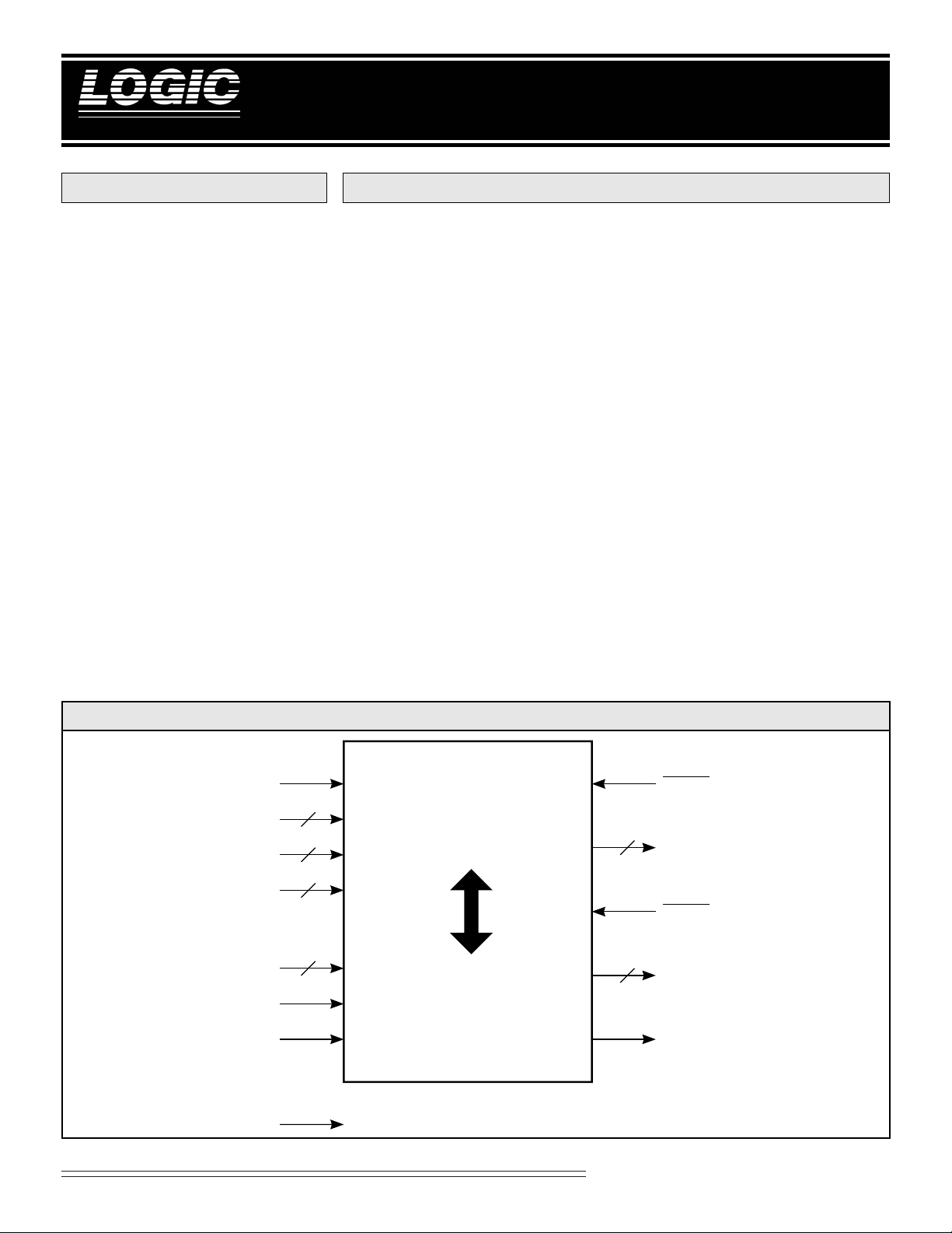
L2330 BLOCK DIAGRAM
ENXR
XRIN
ENYP
YPIN
ACC
TCXY
RTP
CLK
15-0
1-0
31-0
1-0
16
32
OERX
2
2
POLAR
RECTANGULAR
16
16
RXOUT
OEPY
PYOUT
OVF
15-0
15-0
Special Arithmetic Functions
1
09/27/2001–LDS.2330-E
DEVICES INCORPORATED
L2330
Coordinate T ransf ormer
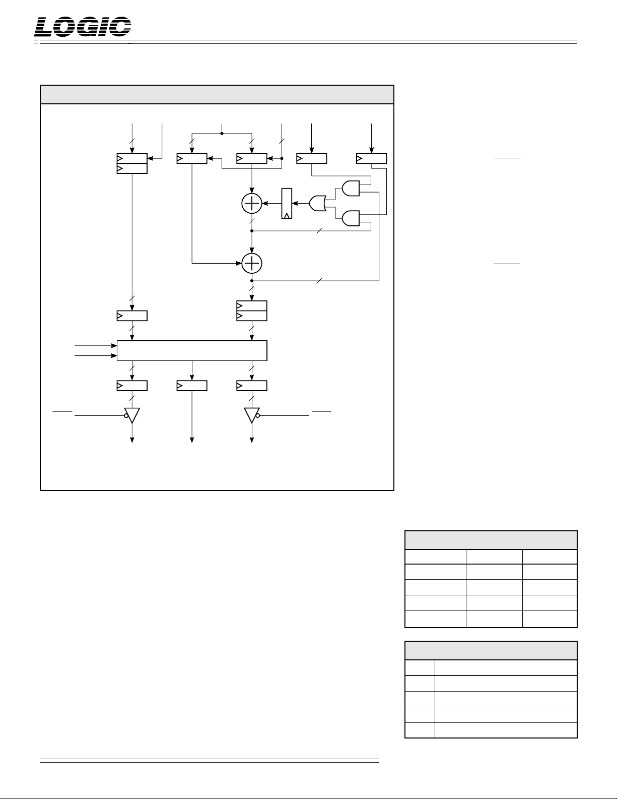
L2330 FUNCTIONAL BLOCK DIAGRAM
15-0
XRIN
16
16
16
TCXY
RTP
16
16
OERX
ENXR ENYP
AM
TRANSFORM
*
PROCESSOR
YPIN
32
MC
31-0
Outputs
RXOUT15-0 — x-coordinate/Magnitude
1-0
ACC
1
32
2
ACC
0
Data Output
RXOUT15-0 is the 16-bit Cartesian
x-coordinate/Polar Magnitude Data
output port. When OERX is HIGH,
RXOUT15-0 is forced into the highimpedance state.
32
PM
32
PYOUT15-0 — y-coordinate/Phase Angle
Data Output
PYOUT15-0 is the 16-bit Cartesian
y-coordinate/Polar Phase Angle Data
FM
**
n
**
n
32
output port. When OEPY is HIGH,
PYOUT15-0 is forced into the highimpedance state.
Controls
ENXR — x-coordinate/Magnitude Data
Input Enable
16
When ENXR is HIGH, XRIN is latched
into the input register on the rising
16
edge of clock. When ENXR is LOW,
the value stored in the register is
OEPY
unchanged.
RXOUT
15-0
REQUIRES 18 CYCLES TO COMPLETE AND IS FULLY PIPELINED*
WHEN RTP IS HIGH ’n’ IS 16-BITS, WHEN RTP IS LOW ’n’ IS 24-BITS**
OVF
SIGNAL DEFINITIONS
Power
VCC and GND
+5V power supply. All pins must be
connected.
Clock
CLK — Master Clock
The rising edge of CLK strobes all
enabled registers.
PYOUT
15-0
Inputs
XRIN15-0 — x-coordinate/Magnitude
Data Input
XRIN15-0 is the 16-bit Cartesian
x-coordinate/Polar Magnitude Data
input port. XRIN15-0 is latched on the
rising edge of CLK.
YPIN31-0 — y-coordinate/Phase Angle
Data Input
YPIN31-0 is the 32-bit Cartesian
y-coordinate/Polar Phase Angle Data
input port. When RTP is HIGH, the input
accumulators should not be used. When
ACC is LOW, the upper 16 bits of YPIN
are the input port and the lower 16 bits
become “don’t cares”. YPIN31-0 is latched
on the rising edge of CLK.
ENYP1-0 — y-coordinate/Phase Angle
Data Input Control
ENYP1-0 is the 2-bit y-coordinate/
Phase Angle Data Input Control that
determines four modes as shown in
TABLE 1. REGISTER OPERATION
ENYP1-0 MC
0 0 Hold Hold
0 1 Load Hold
1 0 Hold Load
1 1 Clear Load
TABLE 2. ACCUMULATOR CONTROL
ACC1-0 Configuration
0 0 No accumulation (normal operation)
0 1 PM accumulator path enabled
1 0 FM accumulator path enabled
1 1 Logical OR of PM and FM (Nonsensical)
Special Arithmetic Functions
2
09/27/2001–LDS.2330-E
DEVICES INCORPORATED
L2330
Coordinate Transformer
Table 1. ‘M’ is the Modulation
Register and ‘C’ is the Carrier Register
as shown in the Functional Block
Diagram.
RTP — Rectangular-to-Polar
When RTP is HIGH, Rectangular-toPolar conversion mode is selected.
When RTP is LOW, Polar-to-Rectangular conversion mode is selected.
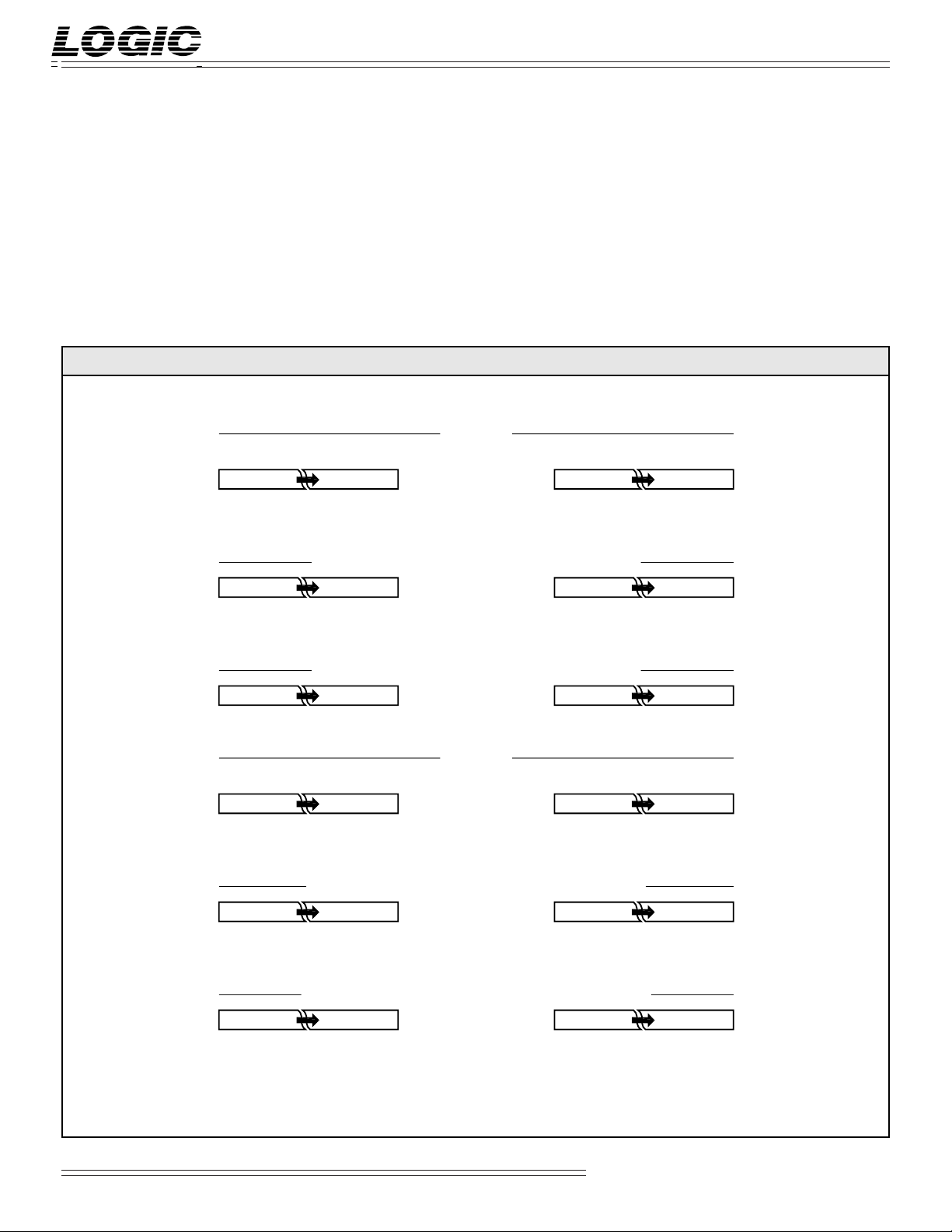
FIGURE 1A.INPUT FORMATS
XRIN YPIN
15 14 13 2 1 0
2152142
15 14 13 2 1 0
NS 2142
13
13
ACC1-0 — Accumulator Control
ACC1-0 is the 2-bit accumulator
control that determines four modes as
shown in Table 2. Changing of the
internal phase Accumulator structure
is very useful when RTP is LOW
allowing for waveform synthesis and
modulation. ACC1-0 set to ‘00’ is most
commonly used when RTP is HIGH
(RTP = 0)
Fract. Unsigned Mag./Two's Comp.Integer Unsigned Magnitude
22212
0
Integer Signed Magnitude (RTP = 1, TCXY = 0)
22212
0
31 30 29 2 1 0
*±202–12
–2
31 30 29 18 17 16
NS 2142
13
unless performing backward mapping
from Cartesian to Polar coordinates.
TCXY — Data Input/Output Format
Select
When TCXY is HIGH, two’s complement format is selected. When TCXY
is LOW, sign-and-magnitude format is
selected.
–292–302–31
2
22212
0
Integer Two's Complement (RTP = 1, TCXY = 1)
15 14 13 2 1 0
–2152142
13
22212
0
31 30 29 18 17 16
–2152142
13
22212
(RTP = 0)
Fractional Unsigned Magnitude
15 14 13 2 1 0
202–12
–2
–132–142–15
2
Fract. Unsigned Mag./Two's Comp.
31 30 29 2 1 0
*±202–12
–2
–292–302–31
2
Fractional Signed Magnitude (RTP = 1, TCXY = 0)
15 14 13 2 1 0
NS 2–12
–2
–132–142–15
2
31 30 29 18 17 16
NS 2–12
–2
–132–142–15
2
Fractional Two's Complement (RTP = 1, TCXY = 1)
15 14 13 2 1 0
–202–12
*±20 denotes two's complement sign or highest magnitude bit. Since phase angles are modulo 2π
and phase accumulator is modulo 232, this bit may be regarded as ±π.
NS denotes negative sign. (i.e. '1' negates the number)
–2
–132–142–15
2
31 30 29 18 17 16
–202–12
–2
–132–142–15
2
0
Special Arithmetic Functions
3
09/27/2001–LDS.2330-E
DEVICES INCORPORATED
L2330
Coordinate T ransf ormer
OVF — Overflow Flag
OVF will go HIGH on the clock the
magnitude of either of the current
Cartesian coordinate outputs exceed
the maximum range. OVF will return
LOW on the clock that the Cartesian
output value(s) return within range.
An overflow condition can only occur
when RTP is LOW.
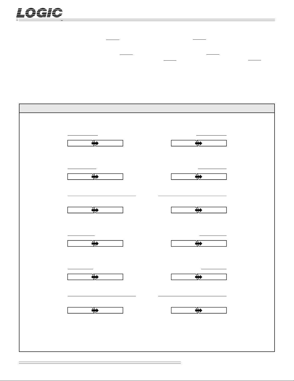
FIGURE 1B.OUTPUT FORMATS
RXOUT PYOUT
15 14 13 2 1 0
NS 2142
15 14 13 2 1 0
–2152142
13
13
OERX — x-coordinate/Magnitude Data
Output Enable
When OERX is LOW, RXOUT15-0 is
enabled for output. When OERX is
HIGH, RXOUT15-0 is placed in a
high-impedance state.
Integer Signed Magnitude (RTP = 0, TCXY = 0)
22212
0
Integer Two's Complement (RTP = 0, TCXY = 1)
22212
0
15 14 13 2 1 0
NS 2142
13
15 14 13 2 1 0
–2152142
13
OEPY — y-coordinate/Phase Angle Data
Output Enable
When OEPY is LOW, PYOUT15-0 is
enabled for output. When OEPY is
HIGH, PYOUT15-0 is placed in a
high-impedance state.
22212
22212
0
0
(RTP = 1)
Fract. Unsigned Mag./Two's Comp.Integer Unsigned Magnitude
15 14 13 2 1 0
2152142
13
22212
0
15 14 13 2 1 0
*±202–12
–2
–132–142–15
2
Fractional Signed Magnitude (RTP = 0, TCXY = 0)
15 14 13 2 1 0
NS 2–12
–2
–132–142–15
2
15 14 13 2 1 0
NS 2–12
–2
–132–142–15
2
Fractional Two's Complement (RTP = 0, TCXY = 1)
15 14 13 2 1 0
–202–12
–2
–132–142–15
2
15 14 13 2 1 0
–202–12
–2
–132–142–15
2
(RTP = 1)
Fract. Unsigned Mag./Two's Comp.Fractional Unsigned Magnitude
15 14 13 2 1 0
202–12
*±20 denotes two's complement sign or highest magnitude bit. Since phase angles are modulo 2π
and phase accumulator is modulo 232, this bit may be regarded as ±π
NS denotes negative sign. (i.e. '1' negates the number)
–2
–132–142–15
2
15 14 13 2 1 0
*±202–12
–2
–132–142–15
2
.
Special Arithmetic Functions
4
09/27/2001–LDS.2330-E
DEVICES INCORPORATED
L2330
Coordinate Transformer
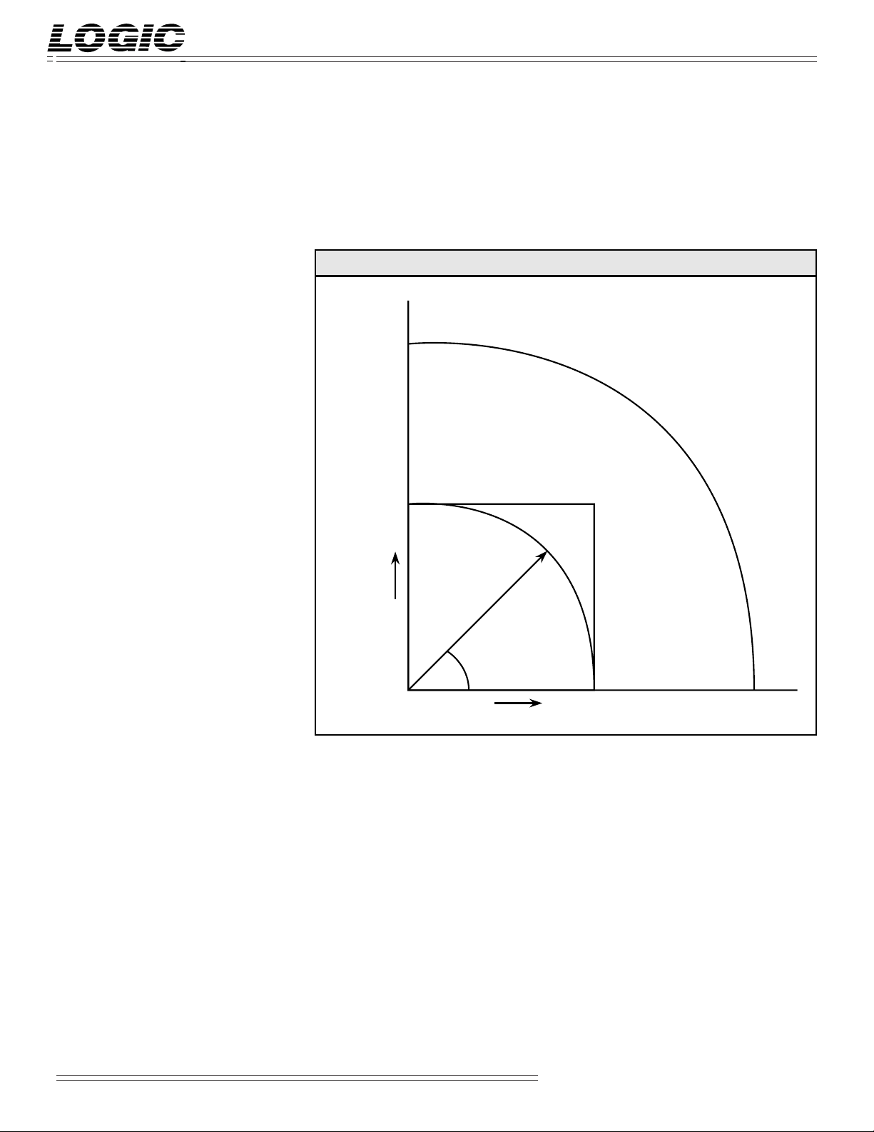
Conversion Ranges
The L2330 supports 16-bit unsigned
radii and 16-bit signed Cartesian
coordinates. Since the 16-bit rectangular
coordinate space does not completely
cover the polar space defined by 16-bit
radii, certain values of “r” will not map
correctly. This condition is indicated by
the overflow (OVF) flag.
In Polar-to-Rectangular conversions, no
overflow occurs for r ≤ 32767 (7FFFH).
Overflow will always occur when r >
46341 (B505H). Note that in signed
magnitude mode r = 46340 (B504H)
will also cause an overflow. For 32767 ≤
r ≤ 46340, overflow may occur depending on the exact values of r and θ.
Figure 2 shows, for the first quadrant,
these three regions: A = no overflow
(correct conversion), B = possible
overflow, C = overflow. The other
quadrants are mapped in a similar
manner.
complement number system is not
symmetric about zero. For example, if
the X or Y component of the input is
–32768 (8000H), no overflow occurs.
But if the X or Y component of the
input is +32768, overflow does occur.
FIGURE 2. CONVERSION RANGES
π/2
65535
32767
When converting from Rectangular-toPolar, if both inputs are zero the radius
is zero but the angle is not defined.
The L2330 will output 4707H in this
case. Since the angle is not defined for a
zero length vector, this is not an error.
C
B
When in signed magnitude mode, the
overflows on the other three quadrants
are the same as in the first. This occurs
because the signed magnitude number
system is symmetric about zero. For
example, if a given r and angle θ cause
an overflow, the same r will cause an
overflow for the angles -θ, π+θ , π-θ.
However, when in two’s complement
mode, the overflows aren’t quite the
same. This occurs because the two’s
A
y
r
θ
x
32767
65535
Special Arithmetic Functions
5
09/27/2001–LDS.2330-E
DEVICES INCORPORATED
L2330
Coordinate T ransf ormer
Internal Precision
When performing a coordinate
transformation, inaccuracies are
introduced by a combination of
quantization and approximation
errors. The accuracy of a coordinate
transformer is dependent on the
word length used for the input
variables, the word length used for
internal calculations, as well as the
number of iterations or steps performed. Truncation errors are due
to the finite word length, and
approximation errors are due to the
finite number of iterations. For
example, in the case of performing a
polar-to-rectangular transformation,
the accuracy of the rotation will be
determined by how closely the input
rotation angle was approximated by
the summation of sub-rotation
angles.
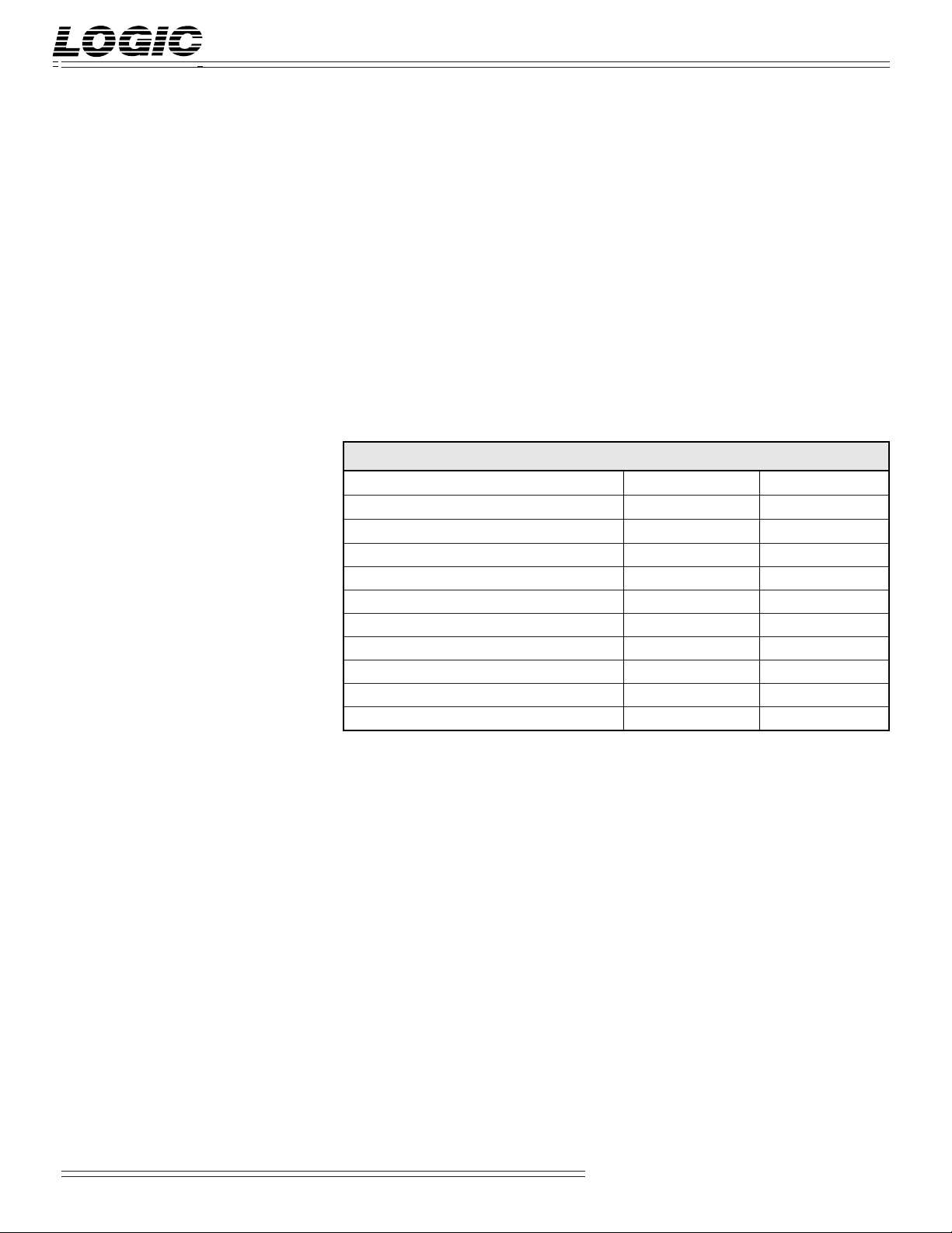
In this study, we examine the
effectiveness of 16-bit internal
precision versus 24-bit internal
precision. 10,000 random Rectangular coordinates were converted to
Polar and back to Rectangular. The
resulting Rectangular coordinates
from this double conversion were
then compared to the original
Rectangular coordinates input to the
device. These vectors, with maximum word width of 16-bits, were
sent through a 16-bit internal
processor versus a 24-bit internal
processor. The Rectangular coordinates were limited to the following
conditions:
–32769<x<32768
–32769<y<32768
Using the 16-bit internal processor, the
resulting Rectangular coordinates were
compared to the original Rectangular
coordinates (see Table 3). Using the 24bit internal processor, the resulting
Rectangular coordinates were compared to the original Rectangular
coordinates (see Table 3). By way of
comparison between the 16-bit internal
processor and the 24-bit internal
processor, we find that the 24-bit
internal processor is significantly more
accurate. This accuracy is due to
internal word length. During coordinate transformation, the number of bits
truncated within a 24-bit internal
processor are much smaller than in a
16-bit internal processor resulting in
smaller error.
TABLE 3. DOUBLE CONVERSION ERROR
Error Internal 16-bit Internal 24-bit
Mean Error (X) 0.0216 –0.0118
Mean Error (Y) –0.0036 –0.0028
Mean Absolute Error (X) 1.5736 0.5116
Mean Absolute Error (Y) 1.0756 0.5160
Root Mean Square Error (X) 2.0168 0.7664
Root Mean Square Error (Y) 1.4356 0.7738
Max Error (X) 6.0/–7.0 3.0/–3.0
Max Error (Y) 5.0/–5.0 3.0/–3.0
Standard Deviation of Error (X) 2.0168 0.7664
Standard Deviation of Error (Y) 1.4357 0.7739
Special Arithmetic Functions
6
09/27/2001–LDS.2330-E

DEVICES INCORPORATED
L2330
Coordinate Transformer
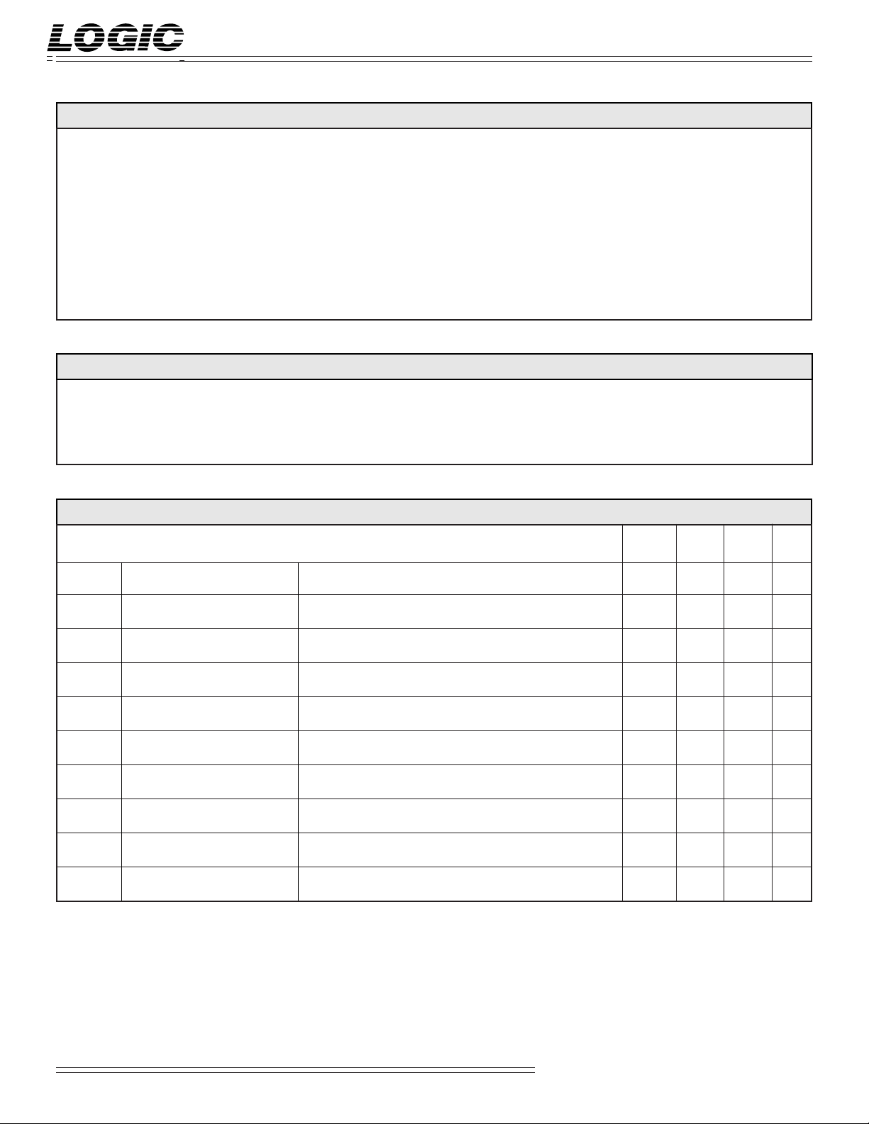
Circle Test
When performing a polar-to-rectangular transformation, a 24-bit internal
processor proves to be significantly
more accurate than a 16-bit internal
processor.
In this study, we compare how accurately a coordinate transformer with a
16-bit internal processor versus a 24-bit
internal processor can calculate all the
coordinates of a circle. By setting the
radius to 7FFFH (maximum before
overflow), θ is incremented using the
accumulator of the L2330 in steps of
0000 4000H until all the points of a full
circle are calculated into rectangular
coordinates.
The resulting rectangular coordinates
were plotted and graphed. A graphical
representation of the resulting vectors
for both 16-bit and 24-bit internal
processors are compared near 45°.
Theoretically, a perfect circle is the
desired output but when the resulting
vectors from a coordinate transformer
with 16-bit internal processor are
graphed and displayed as shown in
Figure 3, we see significant errors due
to the inherent properties of a digital
coordinate transformation system. In
comparison, the 24-bit internal processor proves to be significantly more
accurate than a 16-bit internal processor
due to minimization of truncation
errors. In many applications, this
margin of error is of great significance
especially when being used in applications such as medical ultrasound or
modulation techniques.
step resolution on a 24-bit internal
processor is 1 unit in the x and y thus
resulting in greater accuracy.
The minimum theoretical angle resolution that could be produced is 0.00175°
when x = 7FFFH and y = 1H. A 16-bit
internal processor can produce a
minimum angle resolution of only
0.00549° and will not be able to properly calculate the theoretical minimum
angle resolution. On the other hand, a
24-bit internal processor can produce a
minimum angle resolution of 0.00002°
and could therefore properly calculate
the theoretical minimum angle resolution.
FIGURE 3. CIRCLE TEST RESULT NEAR 45° (16-BIT INTERNAL PROCESSOR)
23200
23190
23180
23170
Y
23160
23150
23140
23140 23150 23160 23170 23180 23190 23200
X
FIGURE 4. CIRCLE TEST RESULT NEAR 45° (24-BIT INTERNAL PROCESSOR)
23200
23190
23180
23170
Y
23160
Data values for Figure 3 and Figure 4
are shown in Table 4. By looking at
these values, we observe the step
resolution on a 16-bit internal processor
is not 1 unit in the x and y. In most
cases, the minimum step resolution is 2
units in the x and y. On the other hand,
23150
23140
23140 23150 23160 23170 23180 23190 23200
X
Special Arithmetic Functions
7
09/27/2001–LDS.2330-E

DEVICES INCORPORATED
TABLE 4. R ESULTANT DATA VALUES OF CIRCLE TEST NEAR 45°
16-bit Internal Processor 24-bit Internal Processor
x x (HEX) y y (HEX) x x (HEX) y y (HEX)
23201 5AA1 23139 5A63 23199 5A9F 23140 5A64
23199 5A9F 23141 5A65 23198 5A9E 23141 5A65
23199 5A9F 23141 5A65 23198 5A9E 23141 5A65
23199 5A9F 23141 5A65 23197 5A9D 23142 5A66
23199 5A9F 23141 5A65 23197 5A9D 23142 5A66
23197 5A9D 23143 5A67 23196 5A9C 23143 5A67
23197 5A9D 23143 5A67 23196 5A9C 23143 5A67
23197 5A9D 23143 5A67 23195 5A9B 23144 5A68
23197 5A9D 23143 5A67 23194 5A9A 23145 5A69
23195 5A9B 23145 5A69 23194 5A9A 23145 5A69
23195 5A9B 23145 5A69 23194 5A9A 23145 5A69
23195 5A9B 23145 5A69 23193 5A99 23146 5A6A
23195 5A9B 23145 5A69 23192 5A98 23147 5A6B
23192 5A98 23148 5A6C 23191 5A97 23148 5A6C
23192 5A98 03148 5A6C 23191 5A97 23148 5A6C
23192 5A98 23148 5A6C 23191 5A97 23148 5A6C
23192 5A98 23148 5A6C 23190 5A96 23149 5A6D
23190 5A96 23150 5A6E 23189 5A95 23150 5A6E
23190 5A96 23150 5A6E 23189 5A95 23150 5A6E
23190 5A96 23150 5A6E 23189 5A95 23150 5A6E
23190 5A96 23150 5A6E 23188 5A94 23151 5A6F
23187 5A93 23152 5A70 23187 5A93 23152 5A70
23187 5A93 23152 5A70 23186 5A92 23153 5A71
23187 5A93 23152 5A70 23186 5A92 23153 5A71
23187 5A93 23152 5A70 23186 5A92 23153 5A71
23185 5A91 23154 5A72 23185 5A91 23154 5A72
23185 5A91 23154 5A72 23184 5A90 23155 5A73
23185 5A91 23154 5A72 23184 5A90 23155 5A73
23185 5A91 23154 5A72 23184 5A90 23155 5A73
23183 5A8F 23156 5A74 23183 5A8F 23156 5A74
L2330
Coordinate T ransf ormer
Special Arithmetic Functions
8
09/27/2001–LDS.2330-E
DEVICES INCORPORATED
L2330
Coordinate Transformer
MAXIMUM RATINGS
Storage temperature ........................................................................................................... –65°C to +150°C
Operating ambient temperature........................................................................................... –55°C to +125°C
VCC supply voltage with respect to ground............................................................................ –0.5 V to +7.0V
Input signal with respect to ground ............................................................................... –0.5 V to VCC + 0.5 V
Signal applied to high impedance output ...................................................................... –0.5 V to VCC + 0.5 V
Output current into low outputs............................................................................................................. 25 mA
Latchup current ............................................................................................................................... > 400 mA
OPERATING CONDITIONS
Active Operation, Commercial 0°C to +70°C 4.75 V ≤ VCC ≤ 5.25 V
Active Operation, Military –55°C to +125°C 4.50 V ≤ VCC ≤ 5.50V
ELECTRICAL CHARACTERISTICS
Above which useful life may be impaired (Notes 1, 2, 3, 8)
To meet specified electrical and switching characteristics
Mode Temperature Range (Ambient) Supply Voltage
Over Operating Conditions (Note 4)
Symbol Parameter Test Condition Min Typ Max Unit
VOH Output High Voltage VCC = Min., IOH = –2.0 mA 2.4 V
VOL Output Low Voltage VCC = Min., IOL = 4.0 mA 0.4 V
VIH Input High Voltage 2.0 VCC V
VIL Input Low Voltage (Note 3) 0.0 0.8 V
IIX Input Current Ground ≤ VIN ≤ VCC (Note 12) ±10 µA
IOZ Output Leakage Current Ground ≤ VOUT ≤ VCC (Note 12) ±10 µA
ICC1 VCC Current, Dynamic (Notes 5, 6) 95 mA
ICC2 VCC Current, Quiescent (Note 7) 5mA
CIN Input Capacitance TA = 25°C, f = 1 MHz 10 pF
COUT Output Capacitance TA = 25°C, f = 1 MHz 10 pF
Special Arithmetic Functions
9
09/27/2001–LDS.2330-E
DEVICES INCORPORATED
4
4
4
4
4
4
4
4
4
4
4
4
4
4
4
4
4
4
4
4
4
4
4
4
4
4
4
4
4
4
6
6
6
6
6
6
6
6
6
6
6
6
6
6
6
6
6
6
6
6
6
6
6
6
6
6
6
6
6
6
4
4
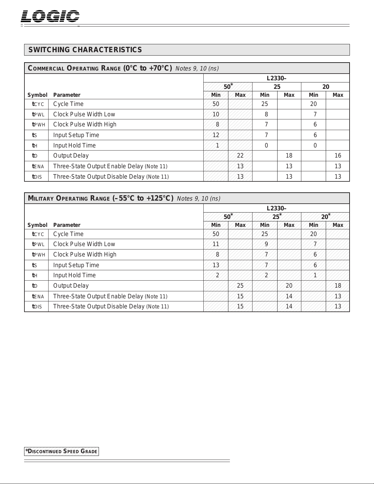
SWITCHING CHARACTERISTICS
L2330
Coordinate T ransf ormer
COMMERCIAL OPERATING RANGE (0°C to +70°C)
Symbol Parameter Min Max Min Max Min Max
tCYC Cycle Time 50 25 20
tPWL Clock Pulse Width Low 10 8 7
tPWH Clock Pulse Width High 8 7 6
tS Input Setup Time 12 7 6
tH Input Hold Time 1 0 0
tD Output Delay 22 18 16
tENA Three-State Output Enable Delay (Note 11) 13 13 13
tDIS Three-State Output Disable Delay (Note 11) 13 13 13
MILITARY OPERATING RANGE (–55°C to +125°C)
Symbol Parameter Min Max Min Max Min Max
tCYC Cycle Time 50 25 20
tPWL Clock Pulse Width Low 11 9 7
tPWH Clock Pulse Width High 8 7 6
tS Input Setup Time 13 7 6
tH Input Hold Time 2 2 1
tD Output Delay 25 20 18
tENA Three-State Output Enable Delay (Note 11) 15 14 13
tDIS Three-State Output Disable Delay (Note 11) 15 14 13
Notes 9, 10 (ns)
23456789012345
23456789012345
23456789012345
23456789012345
23456789012345
23456789012345
23456789012345
23456789012345
23456789012345
23456789012345
23456789012345
23456789012345
23456789012345
23456789012345
23456789012345
23456789012345
23456789012345
23456789012345
23456789012345
23456789012345
23456789012345
23456789012345
23456789012345
23456789012345
23456789012345
23456789012345
23456789012345
23456789012345
23456789012345
23456789012345
Notes 9, 10 (ns)
23456789012345678901234567890121234567890123
23456789012345678901234567890121234567890123
23456789012345678901234567890121234567890123
23456789012345678901234567890121234567890123
23456789012345678901234567890121234567890123
23456789012345678901234567890121234567890123
23456789012345678901234567890121234567890123
23456789012345678901234567890121234567890123
23456789012345678901234567890121234567890123
23456789012345678901234567890121234567890123
23456789012345678901234567890121234567890123
23456789012345678901234567890121234567890123
23456789012345678901234567890121234567890123
23456789012345678901234567890121234567890123
23456789012345678901234567890121234567890123
23456789012345678901234567890121234567890123
23456789012345678901234567890121234567890123
23456789012345678901234567890121234567890123
23456789012345678901234567890121234567890123
23456789012345678901234567890121234567890123
23456789012345678901234567890121234567890123
23456789012345678901234567890121234567890123
23456789012345678901234567890121234567890123
23456789012345678901234567890121234567890123
23456789012345678901234567890121234567890123
23456789012345678901234567890121234567890123
23456789012345678901234567890121234567890123
23456789012345678901234567890121234567890123
23456789012345678901234567890121234567890123
23456789012345678901234567890121234567890123
50
50
L2330–
*
25 20
L2330–
*
25
*
20
*
2345678901234567890123
2345678901234567890123
*DISCONTINUED SPEED GRADE
10
Special Arithmetic Functions
09/27/2001–LDS.2330-E

DEVICES INCORPORATED
SWITCHING WAVEFORMS:NO ACCUMULATION
L2330
Coordinate Transformer
01232223
CLK
t
H
t
RTP
S
TCXY
ACC
ENXR
ENYP
XRIN
YPIN
RXOUT
PYOUT
1-0
1-0
15-0
31-0
15-0
15-0
00 00 00
EN EN EN
A B C
SWITCHING WAVEFORMS:PHASE MODULATION
CLK
RTP, TCXY
ACC
ENXR
1-0
0123422
00 01
01 01
24
t
t
PWL
CYC
t
PWH
D
t
f(A) f(B)
23
01
24 25
XRIN
ENYP
YPIN
RXOUT
PYOUT
15-0
31-0
15-0
15-0
R
1-0
10
C
01 01 01
I J K
01
L
C + I 2C + J 3C + K 4C + L
Special Arithmetic Functions
11
09/27/2001–LDS.2330-E

DEVICES INCORPORATED
S1
I
OH
I
OL
V
TH
C
L
DUT
OE
0.2 V
t
DIS
t
ENA
0.2 V
1.5 V 1.5 V
3.5V Vth
1
Z
0
Z
Z
1
Z
0
1.5 V
1.5 V
0V Vth
VOL*
V
OH
*
V
OL
*
V
OH
*
Measured V
OL
with IOH = –10mA and IOL = 10mA
Measured V
OH
with IOH = –10mA and IOL = 10mA
NOTES
L2330
Coordinate T ransf ormer
1. Maximum Ratings indicate stress
specifications only. Functional operation of these products at values beyond those indicated in the Operating
Conditions table is not implied. Exposure to maximum rating conditions for
extended periods may affect reliability.
2. The products described by this specification include internal circuitry designed to protect the chip from damaging substrate injection currents and accumulations of static charge. Nevertheless, conventional precautions
should be observed during storage,
handling, and use of these circuits in
order to avoid exposure to excessive
electrical stress values.
3. This device provides hard clamping
of transient undershoot and overshoot.
Input levels below ground or above
VCC will be clamped beginning at –
0.6 V and VCC + 0.6 V. The device can
withstand indefinite operation with inputs in the range of –0.5 V to +7.0 V.
Device operation will not be adversely
affected, however, input current levels
will be well in excess of 100 mA.
9. AC specifications are tested with
input transition times less than 3 ns,
output reference levels of 1.5 V (except
tDIS test), and input levels of nominally
0 to 3.0 V. Output loading may be a
resistive divider which provides for
specified IOH and IOL at an output
voltage of VOH min and VOL max
respectively. Alternatively, a diode
bridge with upper and lower current
sources of IOH and IOL respectively,
and a balancing voltage of 1.5 V may be
used. Parasitic capacitance is 30 pF
minimum, and may be distributed.
This device has high-speed outputs capable of large instantaneous current
pulses and fast turn-on/turn-off times.
As a result, care must be exercised in the
testing of this device. The following
measures are recommended:
a. A 0.1 µF ceramic capacitor should be
installed between VCC and Ground
leads as close to the Device Under Test
(DUT) as possible. Similar capacitors
should be installed between device VCC
and the tester common, and device
ground and tester common.
11. For the tENA test, the transition is
measured to the 1.5 V crossing point
with datasheet loads. For the tDIS test,
the transition is measured to the
±200mV level from the measured
steady-state output voltage with
±10mA loads. The balancing voltage, VTH, is set at 3.5 V for Z-to-0
and 0-to-Z tests, and set at 0 V for Zto-1 and 1-to-Z tests.
12. These parameters are only tested at
the high temperature extreme, which is
the worst case for leakage current.
FIGURE A. OUTPUT LOADING CIRCUIT
FIGURE B. THRESHOLD LEVELS
4. Actual test conditions may vary
from those designated but operation is
guaranteed as specified.
5. Supply current for a given application
can be accurately approximated by:
2
NCV F
where
4
N = total number of device outputs
C = capacitive load per output
V = supply voltage
F = clock frequency
6. Tested with all outputs changing every cycle and no load, at a 20 MHz clock
rate.
7. Tested with all inputs within 0.1 V of
VCC or Ground, no load.
8. These parameters are guaranteed
but not 100% tested.
b. Ground and VCC supply planes
must be brought directly to the DUT
socket or contactor fingers.
c. Input voltages should be adjusted to
compensate for inductive ground and VCC
noise to maintain required DUT input
levels relative to the DUT ground pin.
10. Each parameter is shown as a minimum or maximum value. Input requirements are specified from the point
of view of the external system driving
the chip. Setup time, for example, is
specified as a minimum since the external system must supply at least that
much time to meet the worst-case requirements of all parts. Responses from
the internal circuitry are specified from
the point of view of the device. Output
delay, for example, is specified as a
maximum since worst-case operation of
any device always provides data within
that time.
12
Special Arithmetic Functions
09/27/2001–LDS.2330-E

DEVICES INCORPORATED
ORDERING INFORMATION
120-pin
PYOUT5PYOUT6GND
PYOUT7PYOUT8PYOUT9GND
PYOUT10PYOUT11PYOUT12VCCPYOUT13PYOUT14PYOUT15GND
OVF
RXOUT0RXOUT1VCCRXOUT2RXOUT3RXOUT4GND
Coordinate Transformer
RXOUT5RXOUT6RXOUT7GND
RXOUT8RXOUT9V
CC
L2330
V
PYOUT
PYOUT
GND
PYOUT
PYOUT
PYOUT
V
OEPY
GND
RTP
CLK
GND
TCXY
ENYP
GND
ENYP
ACC
ACC
V
YPIN
YPIN
YPIN
YPIN
YPIN
YPIN
YPIN
GND
YPIN
YPIN
120
119
118
117
116
115
114
113
112
111
110
109
108
107
106
105
104
CC
1
4
2
3
3
4
2
5
6
1
7
0
8
CC
9
10
11
12
13
14
15
0
16
17
1
18
0
19
1
20
CC
21
0
22
1
23
2
24
3
25
4
26
5
27
6
28
29
7
30
8
3132333435363738394041424344454647484950515253545556575859
9
10
CC
V
GND
YPIN
YPIN
YPIN11YPIN12YPIN13YPIN14YPIN15YPIN16YPIN
17
CC
V
Top
View
YPIN18YPIN19YPIN
103
20
21
GND
YPIN22YPIN
YPIN
999897969594939291
102
101
100
23
CC
V
YPIN24YPIN25YPIN26YPIN27YPIN28YPIN29YPIN30YPIN
31
60
0
ENXR
XRIN
90
RXOUT
RXOUT
GND
RXOUT
RXOUT
RXOUT
V
CC
RXOUT
GND
OERX
CC
V
XRIN
XRIN
XRIN
GND
XRIN
XRIN
XRIN
XRIN
XRIN
XRIN
XRIN
GND
XRIN
XRIN
XRIN
GND
XRIN
XRIN
V
CC
10
11
12
13
14
15
15
14
13
12
11
10
9
8
7
6
5
4
3
2
1
89
88
87
86
85
84
83
82
81
80
79
78
77
76
75
74
73
72
71
70
69
68
67
66
65
64
63
62
61
Speed
25 ns
20 ns
Plastic Quad Flatpack
(Q1)
0°C to +70°C — COMMERCIAL SCREENING
L2330QC25
L2330QC20
Special Arithmetic Functions
13
09/27/2001–LDS.2330-E

DEVICES INCORPORATED
1
1
1
1
1
1
1
1
1
1
1
1
1
1
1
1
1
1
1
1
1
1
1
1
1
1
1
1
1
1
1
1
1
1
1
1
1
1
1
1
1
1
1
1
1
1
1
1
1
1
1
1
1
1
1
1
1
1
1
1
1
1
1
1
1
1
1
ORDERING INFORMATION
23456789012345678901234567890121234567890123456789012345678901212345678901234567890123456789012
23456789012345678901234567890121234567890123456789012345678901212345678901234567890123456789012
23456789012345678901234567890121234567890123456789012345678901212345678901234567890123456789012
120-pin
23456789012345678901234567890121234567890123456789012345678901212345678901234567890123456789012
23456789012345678901234567890121234567890123456789012345678901212345678901234567890123456789012
23456789012345678901234567890121234567890123456789012345678901212345678901234567890123456789012
23456789012345678901234567890121234567890123456789012345678901212345678901234567890123456789012
23456789012345678901234567890121234567890123456789012345678901212345678901234567890123456789012
23456789012345678901234567890121234567890123456789012345678901212345678901234567890123456789012
23456789012345678901234567890121234567890123456789012345678901212345678901234567890123456789012
23456789012345678901234567890121234567890123456789012345678901212345678901234567890123456789012
23456789012345678901234567890121234567890123456789012345678901212345678901234567890123456789012
23456789012345678901234567890121234567890123456789012345678901212345678901234567890123456789012
23456789012345678901234567890121234567890123456789012345678901212345678901234567890123456789012
23456789012345678901234567890121234567890123456789012345678901212345678901234567890123456789012
23456789012345678901234567890121234567890123456789012345678901212345678901234567890123456789012
23456789012345678901234567890121234567890123456789012345678901212345678901234567890123456789012
23456789012345678901234567890121234567890123456789012345678901212345678901234567890123456789012
23456789012345678901234567890121234567890123456789012345678901212345678901234567890123456789012
23456789012345678901234567890121234567890123456789012345678901212345678901234567890123456789012
23456789012345678901234567890121234567890123456789012345678901212345678901234567890123456789012
23456789012345678901234567890121234567890123456789012345678901212345678901234567890123456789012
23456789012345678901234567890121234567890123456789012345678901212345678901234567890123456789012
23456789012345678901234567890121234567890123456789012345678901212345678901234567890123456789012
23456789012345678901234567890121234567890123456789012345678901212345678901234567890123456789012
23456789012345678901234567890121234567890123456789012345678901212345678901234567890123456789012
23456789012345678901234567890121234567890123456789012345678901212345678901234567890123456789012
23456789012345678901234567890121234567890123456789012345678901212345678901234567890123456789012
23456789012345678901234567890121234567890123456789012345678901212345678901234567890123456789012
23456789012345678901234567890121234567890123456789012345678901212345678901234567890123456789012
23456789012345678901234567890121234567890123456789012345678901212345678901234567890123456789012
23456789012345678901234567890121234567890123456789012345678901212345678901234567890123456789012
23456789012345678901234567890121234567890123456789012345678901212345678901234567890123456789012
23456789012345678901234567890121234567890123456789012345678901212345678901234567890123456789012
23456789012345678901234567890121234567890123456789012345678901212345678901234567890123456789012
23456789012345678901234567890121234567890123456789012345678901212345678901234567890123456789012
23456789012345678901234567890121234567890123456789012345678901212345678901234567890123456789012
23456789012345678901234567890121234567890123456789012345678901212345678901234567890123456789012
23456789012345678901234567890121234567890123456789012345678901212345678901234567890123456789012
23456789012345678901234567890121234567890123456789012345678901212345678901234567890123456789012
23456789012345678901234567890121234567890123456789012345678901212345678901234567890123456789012
23456789012345678901234567890121234567890123456789012345678901212345678901234567890123456789012
23456789012345678901234567890121234567890123456789012345678901212345678901234567890123456789012
23456789012345678901234567890121234567890123456789012345678901212345678901234567890123456789012
23456789012345678901234567890121234567890123456789012345678901212345678901234567890123456789012
23456789012345678901234567890121234567890123456789012345678901212345678901234567890123456789012
23456789012345678901234567890121234567890123456789012345678901212345678901234567890123456789012
23456789012345678901234567890121234567890123456789012345678901212345678901234567890123456789012
23456789012345678901234567890121234567890123456789012345678901212345678901234567890123456789012
23456789012345678901234567890121234567890123456789012345678901212345678901234567890123456789012
23456789012345678901234567890121234567890123456789012345678901212345678901234567890123456789012
23456789012345678901234567890121234567890123456789012345678901212345678901234567890123456789012
23456789012345678901234567890121234567890123456789012345678901212345678901234567890123456789012
23456789012345678901234567890121234567890123456789012345678901212345678901234567890123456789012
23456789012345678901234567890121234567890123456789012345678901212345678901234567890123456789012
23456789012345678901234567890121234567890123456789012345678901212345678901234567890123456789012
23456789012345678901234567890121234567890123456789012345678901212345678901234567890123456789012
23456789012345678901234567890121234567890123456789012345678901212345678901234567890123456789012
23456789012345678901234567890121234567890123456789012345678901212345678901234567890123456789012
23456789012345678901234567890121234567890123456789012345678901212345678901234567890123456789012
23456789012345678901234567890121234567890123456789012345678901212345678901234567890123456789012
23456789012345678901234567890121234567890123456789012345678901212345678901234567890123456789012
23456789012345678901234567890121234567890123456789012345678901212345678901234567890123456789012
23456789012345678901234567890121234567890123456789012345678901212345678901234567890123456789012
23456789012345678901234567890121234567890123456789012345678901212345678901234567890123456789012
23456789012345678901234567890121234567890123456789012345678901212345678901234567890123456789012
23456789012345678901234567890121234567890123456789012345678901212345678901234567890123456789012
Speed
0°C to +70°C — COMMERCIAL SCREENING
–55°C to +125°C — COMMERCIAL SCREENING
–55°C to +125°C — MIL-STD-883 COMPLIANT
12345
A
PYO
7
PYO
PYO
5
B
PYO
4
PYO
PYO
3
C
PYO
2
PYO
1
V
D
PYO
0
OEPY
GND
E
GND
V
RTP
F
GND
CLK
TCXY
G
GND
0
1
ENYP
ENYP
H
V
ACC
ACC
1
0
J
YPI
1
YPI
0
YPI
K
YPI
4
YPI
2
GND
L
GND
YPI
YPI
7
5
M
YPI
YPI
YPI
9
6
N
YPI
10
YPI
8
YPI
CC
CC
CC
6
7 8 9 10 11
PYO
10
PYO
12
PYO
14
8
PYO
9
PYO
6
GND
GND
PYO
PYO
V
CC
OVF
13
GND
11
KEY
Top View
Through Package
(i.e., Component Side Pinout)
3
CC
14
V
CC
YPI
YPI
GND
18
YPI
19
YPI
V
YPI
YPI
13
YPI
11
YPI
12
16
15
YPI
17
Discontinued Package
Ceramic Pin Grid Array
(G4)
14
L2330
Coordinate T ransf ormer
12 13
15
RXO
0
RXO
2
RXO
4
RXO
6
RXO
8
RXO
10
RXO
1
RXO
3
RXO
5
RXO
7
RXO
9
RXO
12
V
CC
GND
GND
V
CC
RXO
11
RXO
13
GND
RXO
14
RXO
15
V
CC
GND
OERX
XRI
XRI
XRI
XRI
XRI
XRI
XRI
YPI
XRI
15
14
12
XRI
13
10
XRI
11
7
XRI
8
5
XRI
6
3
XRI
4
1
XRI
2
30
XRI
0
09/27/2001–LDS.2330-E
V
CC
GND
XRI
9
GND
GND
V
CC
27
YPI
20
YPI
23
YPI
25
21
YPI
22
YPI
24
YPI
YPI
YPI
V
31
CC
28
ENXR
YPI
26
29
Special Arithmetic Functions
 Loading...