


现货库存、技术资料、百科信息、热点资讯,精彩尽在鼎好!
Data Sheet, Rev. 2.0, May 2006
BTS 7970B
High Current PN Half Bridge
TM
NovalithIC
68 A, 7 mΩ + 9 mΩ typ.
Automotive Power
Never stop thinking.

High Current PN Half Bridge
BTS 7970B
Product Summary . . . . . . . . . . . . . . . . . . . . . . . . . . . . . . . . . . . . . . . . . . . . . . . . . . . .2
Basic Features . . . . . . . . . . . . . . . . . . . . . . . . . . . . . . . . . . . . . . . . . . . . . . . . . . . . . . .2
1Overview . . . . . . . . . . . . . . . . . . . . . . . . . . . . . . . . . . . . . . . . . . . . . . . . . . . . . . . . .3
1.1 Block Diagram . . . . . . . . . . . . . . . . . . . . . . . . . . . . . . . . . . . . . . . . . . . . . . . . . . .3
1.2 Terms . . . . . . . . . . . . . . . . . . . . . . . . . . . . . . . . . . . . . . . . . . . . . . . . . . . . . . . . .4
2 Pin Configuration . . . . . . . . . . . . . . . . . . . . . . . . . . . . . . . . . . . . . . . . . . . . . . . . . .5
2.1 Pin Assignment . . . . . . . . . . . . . . . . . . . . . . . . . . . . . . . . . . . . . . . . . . . . . . . . . .5
2.2 Pin Definitions and Functions . . . . . . . . . . . . . . . . . . . . . . . . . . . . . . . . . . . . . . .5
3 Maximum Ratings . . . . . . . . . . . . . . . . . . . . . . . . . . . . . . . . . . . . . . . . . . . . . . . . . .6
Maximum Single Pulse Current . . . . . . . . . . . . . . . . . . . . . . . . . . . . . . . . . . . . . . . . .7
1 Block Description and Characteristics . . . . . . . . . . . . . . . . . . . . . . . . . . . . . . . . .8
1.1 Supply Characteristics . . . . . . . . . . . . . . . . . . . . . . . . . . . . . . . . . . . . . . . . . . . . .8
1.2 Power Stages . . . . . . . . . . . . . . . . . . . . . . . . . . . . . . . . . . . . . . . . . . . . . . . . . . .9
1.2.1 Power Stages - Static Characteristics . . . . . . . . . . . . . . . . . . . . . . . . . . . 10
1.2.2 Switching Times . . . . . . . . . . . . . . . . . . . . . . . . . . . . . . . . . . . . . . . . . . . 11
1.2.3 Power Stages - Dynamic Characteristics . . . . . . . . . . . . . . . . . . . . . . . . 12
1.3 Protection Functions . . . . . . . . . . . . . . . . . . . . . . . . . . . . . . . . . . . . . . . . . . . . .14
1.3.1 Overvoltage Lock Out . . . . . . . . . . . . . . . . . . . . . . . . . . . . . . . . . . . . . . . 14
1.3.2 Undervoltage Shut Down . . . . . . . . . . . . . . . . . . . . . . . . . . . . . . . . . . . . . 14
1.3.3 Overtemperature Protection . . . . . . . . . . . . . . . . . . . . . . . . . . . . . . . . . . 14
1.3.4 Current Limitation . . . . . . . . . . . . . . . . . . . . . . . . . . . . . . . . . . . . . . . . . . 14
1.3.5 Short Circuit Protection . . . . . . . . . . . . . . . . . . . . . . . . . . . . . . . . . . . . . . 16
1.3.6 Electrical Characteristics - Protection Functions . . . . . . . . . . . . . . . . . . . 17
1.4 Control and Diagnostics . . . . . . . . . . . . . . . . . . . . . . . . . . . . . . . . . . . . . . . . . .18
1.4.1 Input Circuit . . . . . . . . . . . . . . . . . . . . . . . . . . . . . . . . . . . . . . . . . . . . . . . 18
1.4.2 Dead Time Generation . . . . . . . . . . . . . . . . . . . . . . . . . . . . . . . . . . . . . . 18
1.4.3 Adjustable Slew Rate . . . . . . . . . . . . . . . . . . . . . . . . . . . . . . . . . . . . . . . 18
1.4.4 Status Flag Diagnosis With Current Sense Capability . . . . . . . . . . . . . . 18
1.4.5 Truth Table . . . . . . . . . . . . . . . . . . . . . . . . . . . . . . . . . . . . . . . . . . . . . . . 20
1.4.6 Electrical Characteristics - Control and Diagnostics . . . . . . . . . . . . . . . . 21
2 Thermal Characteristics . . . . . . . . . . . . . . . . . . . . . . . . . . . . . . . . . . . . . . . . . . . .22
3 Application . . . . . . . . . . . . . . . . . . . . . . . . . . . . . . . . . . . . . . . . . . . . . . . . . . . . . . .23
3.1 Application Example . . . . . . . . . . . . . . . . . . . . . . . . . . . . . . . . . . . . . . . . . . . . .23
3.2 Layout Considerations . . . . . . . . . . . . . . . . . . . . . . . . . . . . . . . . . . . . . . . . . . . .23
4 Package Outlines P-TO-263-7 . . . . . . . . . . . . . . . . . . . . . . . . . . . . . . . . . . . . . . .24
5 Revision History . . . . . . . . . . . . . . . . . . . . . . . . . . . . . . . . . . . . . . . . . . . . . . . . . .25
Data Sheet 1 Rev. 2.0, 2006-05-09

High Current PN Half Bridge
NovalithIC
TM
BTS 7970B
Product Summary
The BTS 7970B is a fully integrated high current half
bridge for motor drive applications. It is part of the
NovalithICTM family containing one p-channel highside
MOSFET and one n-channel lowside MOSFET with an
integrated driver IC in one package. Due to the p-channel
highside switch the need for a charge pump is eliminated
thus minimizing EMI. Interfacing to a microcontroller is
made easy by the integrated driver IC which features
logic level inputs, diagnosis with current sense, slew rate
adjustment, dead time generation and protection against overtemperature, overvoltage,
undervoltage, overcurrent and short circuit.
The BTS 7970B provides a cost optimized solution for protected high current PWM
motor drives with very low board space consumption.
BTS 7970B
P-TO-263-7
Basic Features
• Path resistance of typ. 16 mΩ @25°C
• Low quiescent current of typ. 7 µA @ 25 °C
• PWM capability of up to 25 kHz combined with active freewheeling
• Switched mode current limitation for reduced power dissipation in overcurrent
• Current limitation level of 68 A typ. / 50 A min.
• Status flag diagnosis with current sense capability
• Overtemperature shut down with latch behaviour
• Overvoltage lock out
• Undervoltage shut down
• Driver circuit with logic level inputs
• Adjustable slew rates for optimized EMI
Type Package
BTS 7970B P-TO-263-7
Data Sheet 2 Rev. 2.0, 2006-05-09
High Current PN Half Bridge
BTS 7970B
Overview
1Overview
The BTS 7970B is part of the NovalithIC family containing three separate chips in one
package: One p-channel highside MOSFET and one n-channel lowside MOSFET
together with a driver IC, forming a fully integrated high current half-bridge. All three
chips are mounted on one common leadframe, using the chip on chip and chip by chip
technology. The power switches utilize vertical MOS technologies to ensure optimum on
state resistance. Due to the p-channel highside switch the need for a charge pump is
eliminated thus minimizing EMI. Interfacing to a microcontroller is made easy by the
integrated driver IC which features logic level inputs, diagnosis with current sense, slew
rate adjustment, dead time generation and protection against overtemperature,
overvoltage, undervoltage, overcurrent and short circuit. The BTS 7970B can be
combined with other BTS 7970B to form H-bridge and 3-phase drive configurations.
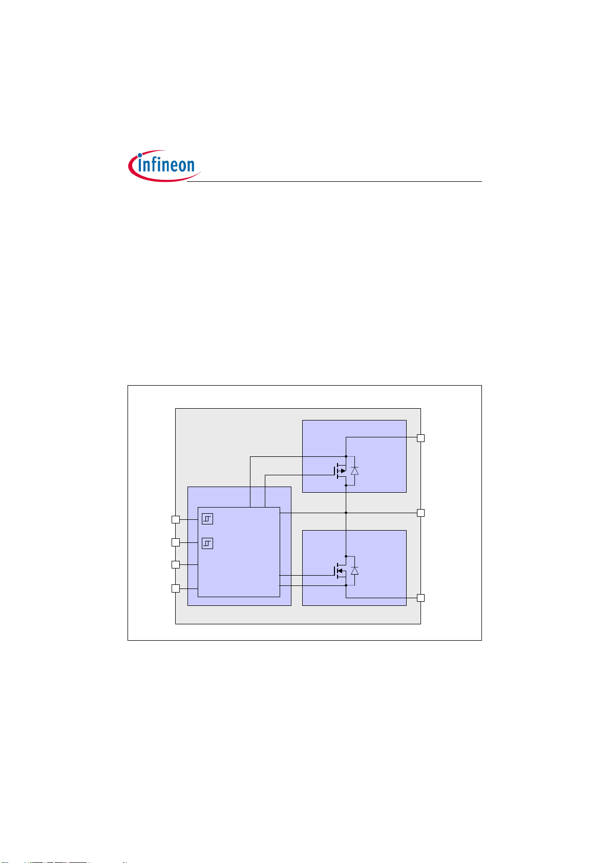
1.1 Block Diagram
BTS 7970B
HS base-chip
VS
Top-chip
IN
INH
SR
IS
Gate Driver
Dead Time Gen.
Slew Rate Adj.
UV Shut Down
OV Lock Out
OT Shut Dow n
Current Lim.
Diagnosis
Current Sense
LS bas e-c hip
OUT
GND
Figure 1 Block Diagram
Data Sheet 3 Rev. 2.0, 2006-05-09

High Current PN Half Bridge
BTS 7970B
1.2 Terms
Following figure shows the terms used in this data sheet.
V
VS ,VS
I
IN
V
IN
I
INH
V
INH
I
SR
V
SR
I
IS
V
IS
Figure 2 Terms
IN
INH
BTS 7970B
SR
IS
VS
GND
I
IVS, -I
D(HS)
GND,ID(LS)
OUT
I
OUT
V
SD (L S)
V
DS(HS)
, I
L
Overview
V
OUT
Data Sheet 4 Rev. 2.0, 2006-05-09

High Current PN Half Bridge
BTS 7970B
2 Pin Configuration
2.1 Pin Assignment
BTS 7970B
P-TO-263-7
8
123567
4
Figure 3 Pin Assignment BTS 7970B and (top view)
Pin Configuration
2.2 Pin Definitions and Functions
Pin Symbol I/O Function
1 GND - Ground
2 IN I Input
Defines whether high- or lowside switch is activated
3 INH I Inhibit
When set to low device goes in sleep mode
4,8 OUT O Power output of the bridge
5 SR I Slew Rate
The slew rate of the power switches can be adjusted
by connecting a resistor between SR and GND
6 IS O Current Sense and Diagnosis
7 VS - Supply
Bold type: Pin needs power wiring
Data Sheet 5 Rev. 2.0, 2006-05-09

High Current PN Half Bridge
BTS 7970B
Maximum Ratings
3 Maximum Ratings
-40 °C < Tj < 150 °C (unless otherwise specified)
Pos Parameter Symbol Limits Unit Test Condition
min max
Electrical Maximum Ratings
3.0.1 Supply voltage
3.0.2 Logic Input Voltage
3.0.3 HS/LS continuous drain
current
3.0.4 HS pulsed drain current I
3.0.5 LS pulsed drain current I
3.0.6 PWM current I
3.0.7 Voltage at SR pin
3.0.8 Voltage between VS and
IS pin
3.0.9 Voltage at IS pin V
Thermal Maximum Ratings
3.0.10 Junction temperature
3.0.11 Storage temperature
ESD Susceptibility
3.0.12 ESD susceptibility
V
VS
V
IN
V
INH
I
D(HS)
I
D(LS)
D(HS)
D(LS)
OUT
V
SR
V
VS -VIS
IS
T
j
T
stg
V
ESD
-0.3 45 V
-0.3 5.3 V
-44 44
1)
A TC < 85°C
switch active
-90 901)A TC < 85°C
= 10ms
t
pulse
-90 901)A
1)
-55 55 A f = 1kHz, DC = 50%
single pulse
-60 60 A f = 20kHz, DC = 50%
-0.3 1.0 V
-0.3 45 V
-20 45 V
-40 150 °C
-55 150 °C
kV HBM
2)
IN, INH, SR, IS
OUT, GND, VS
1)
Maximum reachable current may be smaller depending on current limitation level
2)
ESD susceptibility HBM according to EIA/JESD 22-A 114B
-2
-6
2
6
Note: Maximum ratings are absolute ratings; exceeding any one of these values may
cause irreversible damage to the device. Exposure to maximum rating conditions
for extended periods of time may affect device reliability
Data Sheet 6 Rev. 2.0, 2006-05-09

High Current PN Half Bridge
BTS 7970B
Maximum Single Pulse Current
100
90
80
70
60
[A]
50
max
I
40
30
20
10
0
1,0E-03 1,0E-02 1,0E-01 1,0E+00 1,0E+01
t
pulse
Maximum Ratings
[s]
Figure 4 BTS 7970B Maximum Single Pulse Current
This diagram shows the maximum single pulse current that can be driven for a given
t
pulse time
. The maximum reachable current may be smaller depending on the
pulse
current limitation level. Pulse time may be limited due to thermal protection of the device.
Data Sheet 7 Rev. 2.0, 2006-05-09

High Current PN Half Bridge
BTS 7970B
Block Description and Characteristics
4 Block Description and Characteristics
4.1 Supply Characteristics
T
– 40 °C <
Pos. Parameter Symbol Limit Values Unit Test Conditions
General
4.1.1 Operating Voltage
4.1.2 Supply Current
4.1.3 Quiescent Current I
< 150 °C, 8 V < VS < 18 V, IL = 0A (unless otherwise specified)
j
min. typ. max.
V
S
I
VS(on)
5.5 – 28 V VS increasing
–23mAV
= 5 V
INH
V
= 0 V or 5 V
IN
R
=0 Ω
SR
DC-mode
normal operation
(no fault condition)
VS(off)
–715µAV
––65µA
= 0 V
INH
V
= 0 V or 5 V
IN
T
<85 °C
j
V
= 0 V
INH
V
= 0 V or 5 V
IN
25
[A]
20
VS(of f)
I
15
10
5
0
-40 0 40 80 120 160
[°C]
T
Figure 5 Quiescent Current (typ.) vs. Junction Temperature
Data Sheet 8 Rev. 2.0, 2006-05-09
 Loading...