


现货库存、技术资料、百科信息、热点资讯,精彩尽在鼎好!
TrilithIC
Data Sheet
1Overview
1.1 Features
• Quad D-MOS switch driver
• Free configurable as bridge or quad-switch
• Optimized for DC motor management applications
•Low R
DS ON
side switch (typical values @ 25 C)
• Maximum peak current: typ. 12 A @ 25 C=
• Very low quiescent current: typ. 5 ←A @ 25 C=
• Small outline, enhanced power P-DSO-package
• Full short-circuit-protection
• Operates up to 40 V
• Status flag diagnosis
• Overtemperature shut down with hysteresis
• Internal clamp diodes
• Isolated sources for external current sensing
• Under-voltage detection with hysteresis
• PWM frequencies up to 1 kHz
: 70 mτ high-side switch, 45 mτ low-
BTS 7750 G
P-DSO-28-14
Type Ordering Code Package
BTS 7750 G Q67007-A9401 P-DSO-28-14
1.2 Description
The BTS 7750 G is part of the TrilithIC family containing three dies in one package:
One double high-side switch and two low-side switches. The drains of these three
vertical DMOS chips are mounted on separated leadframes. The sources are connected
to individual pins, so the BTS 7750 G can be used in H-bridge- as well as in any other
configuration. Both the double high-side and the two low-side switches of the
BTS 7750 G are manufactured in SMART SIPMOS
R
vertical DMOS power stages with CMOS control circuitry. The high-side switch is
DS ON
®
technology which combines low
fully protected and contains the control and diagnosis circuitry. Also the low-side
switches are fully protected, the equivalent standard product is the BSP 78.
In contrast to the BTS 7750 GP, which consists of the same chips in an P-TO263-15
package, the P-DSO-28-14 package offers a smaller outline and a lower price for
applications, which do not need the thermal properties of the P-TO263-15.
Data Sheet 1 2001-02-01

1.3 Pin Configuration
(top view)
BTS 7750 G
1DL1
2IL1
3DL1
28 DL1
27 SL1
26 SL1
LS-Leadframe
4N.C.
5DHVS
6GND
7IH1
25 DL1
24 DHVS
23 SH1
22 SH1
HS-Leadframe
8ST
9IH2
21 SH2
20 SH2
N.C.
DL2
DL2
Figure 1
IL2
10DHVS
11
12
13
14
19 DHVS
18 DL2
LS-Leadframe
17 SL2
16 SL2
15 DL2
Data Sheet 2 2001-02-01

BTS 7750 G
1.4 Pin Definitions and Functions
Pin No. Symbol Function
1, 3, 25, 28 DL1 Drain of low-side switch1, leadframe 1
2 IL1 Analog input of low-side switch1
4 N.C. not connected
5, 10, 19, 24 DHVS Drain of high-side switches and power supply voltage,
leadframe 2
1)
6 GND Ground
7 IH1 Digital input of high-side switch1
8 ST Status of high-side switches; open Drain output
9 IH2 Digital input of high-side switch2
11 N.C. not connected
12, 14, 15, 18 DL2 Drain of low-side switch2, leadframe 3
1)
1)
13 IL2 Analog input of low-side switch2
16,17 SL2 Source of low-side switch2
20,21 SH2 Source of high-side switch2
22,23 SH1 Source of high-side switch1
26,27 SL1 Source of low-side switch1
1)
To reduce the thermal resistance these pins are direct connected via metal bridges to the leadframe.
Pins written in bold type need power wiring.
Data Sheet 3 2001-02-01

1.5 Functional Block Diagram
8
ST
BTS 7750 G
DHVS
5,10,19,24
Biasing and ProtectionDiagnosis
IH1
IH2
GND
IL1
IL2
7
13
Driver
OUT
0IN0 L L
0 1 L H
9
6
1 0 H L
1 1 H H
R
O1
Protection
2
Gate
R
O2
20,21
12,14,15,18
22, 23
1,3,25,28
SH2
DL2
SH1
DL1
Driver
Protection
Gate
Driver
26, 27
SL1
16, 17
SL2
Figure 2
Block Diagram
Data Sheet 4 2001-02-01

BTS 7750 G
1.6 Circuit Description
Input Circuit
The control inputs IH1,2 consist of TTL/CMOS compatible Schmitt-Triggers with
hysteresis. Buffer amplifiers are driven by these stages and convert the logic signal into
the necessary form for driving the power output stages. The inputs are protected by ESD
clamp-diodes.
The inputs IL1 and IL2 are connected to the internal gate-driving units of the N-channel
vertical power-MOS-FETs.
Output Stages
The output stages consist of an low
R
Power-MOS H-bridge. In H-bridge
DS ON
configuration, the D-MOS body diodes can be used for freewheeling when commutating
inductive loads. If the high-side switches are used as single switches, positive and
negative voltage spikes which occur when driving inductive loads are limited by
integrated power clamp diodes.
Short Circuit Protection
The outputs are protected against
– output short circuit to ground
– output short circuit to the supply voltage, and
– overload (load short circuit).
An internal OP-Amp controls the Drain-Source-Voltage by comparing the DS-VoltageDrop with an internal reference voltage. Above this trippoint the OP-Amp reduces the
output current depending on the junction temperature and the drop voltage.
In the case of overloaded high-side switches the status output is set to low.
The fully protected low-side switches have no status output.
Overtemperature Protection
The high-side and the low-side switches also incorporate an overtemperature protection
circuit with hysteresis which switches off the output transistors. In the case of the highside switches, the status output is set to low.
Undervoltage-Lockout (UVLO)
V
When
reaches the switch-on voltage V
S
The High-Side output transistors are switched off if the supply voltage
the switch off value
Data Sheet 5 2001-02-01
V
UVOFF.
the IC becomes active with a hysteresis.
UVON
V
drops below
S

BTS 7750 G
Status Flag
The status flag output is an open drain output with Zener-diode which requires a pull-up
resistor, c.f. the application circuit on page 14. Various errors as listed in the table
“Diagnosis” are detected by switching the open drain output ST to low. A open load
detection is not available. Freewheeling condition does not cause an error.
2 Truthtable and Diagnosis (valid only for the High-Side-Switches)
Flag IH1 IH2 SH1 SH2 ST Remarks
Inputs Outputs
Normal operation;
identical with functional truth table
0
0
1
1
0
1
0
1
L
L
H
H
L
H
L
H
1
stand-by mode
1
switch2 active
1
switch1 active
1
both switches
active
Overtemperature high-side switch1 0
1
Overtemperature high-side switch2 X
X
Overtemperature both high-side switches 0
X
1
X
X
0
1
0
1
X
L
L
X
X
L
L
L
X
X
L
L
L
L
L
1
0detected
1
0detected
1
0
detected
0
detected
Undervoltage X X L L 1 not detected
Inputs: Outputs: Status:
0 = Logic LOW Z = Output in tristate condition 1 = No error
1 = Logic HIGH L = Output in sink condition 0 = Error
X = don’t care H = Output in source condition
X = Voltage level undefined
Data Sheet 6 2001-02-01

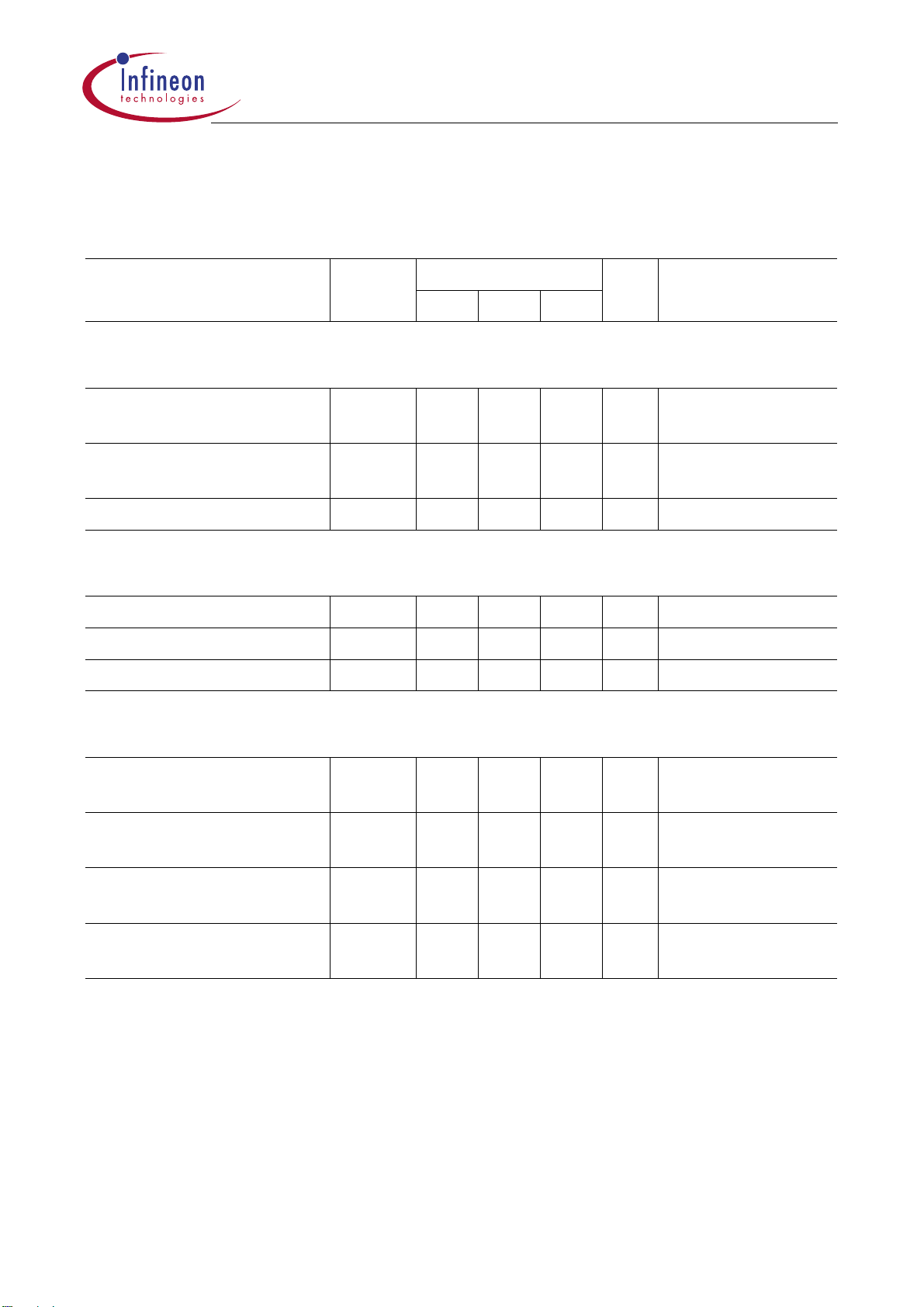
3 Electrical Characteristics
3.1 Absolute Maximum Ratings
T
– 40 C <
< 150 C
j
Parameter Symbol Limit Values Unit Remarks
min. max.
High-Side-Switches (Pins DHVS, IH1,2 and SH1,2)
BTS 7750 G
Supply voltage
Supply voltage for full short
V
S
V
S(SCP)
– 0.3 42 V –
28 V
circuit protection
HS-drain current*
HS-input current
HS-input voltage
I
I
V
S
IH
IH
– 7.5 ** A TA = 25°C; tP < 100 ms
– 5 5 mA Pin IH1 and IH2
– 10 16 V Pin IH1 and IH2
Note: * single pulse ** internally limited
Status Output ST
Status pull up voltage
Status Output current
V
I
ST
ST
– 0.3 5.4 V
– 5 5 mA Pin ST
Low-Side-Switches (Pins DL1,2, IL1,2 and SL1,2)
Drain-Source-Clamp voltage
Supply voltage for short
circuit protection
V
DSL
V
DSL(SCP)
42 – V VIL=0V; ID 1mA
30 V VIL=5V
20 V
V
IL
=10V
LS-drain current*
LS-input voltage
I
V
DL
– 7.5 ** A TA = 25°C; tP < 100 ms
IL
– 0.3 10 V –
Note: * single pulse ** internally limited
Temperatures
Junction temperature
Storage temperature
Data Sheet 7 2001-02-01
T
j
T
stg
– 40 150 C–
– 55 150 C–

3.1 Absolute Maximum Ratings (cont’d)
– 40 C <
T
< 150 C
j
Parameter Symbol Limit Values Unit Remarks
min. max.
Thermal Resistances (one HS-LS-Path active)
BTS 7750 G
LS-junction case
HS-junction case
Junction ambient
R
thja
= T
j(HS)
/(P
(HS)+P(LS)
R
thjC L
R
thjC H
R
thja
)
– 20 K/W measured to pin 3 or 12
– 20 K/W measured to pin 19
– 60 K/W device soldered to
reference PCB with
2
6cm
cooling area
ESD Protection (Human Body Model acc. MIL STD 883D, method 3015.7 and EOS/
ESD assn. standard S5.1 - 1993)
Input LS-Switch
Input HS-Switch
Status HS-Switch
Output LS and HS-Switch
V
V
V
V
ESD
ESD
ESD
ESD
–2kV
–1kV
–2kV
– 8 kV all other pins connected
to Ground
Note: Maximum ratings are absolute ratings; exceeding any one of these values may
cause irreversible damage to the integrated circuit.
3.2 Operating Range
T
– 40 C <
< 150 C
j
Parameter Symbol Limit Values Unit Remarks
min. max.
Supply voltage
Input voltages V
Input voltages
Output current
Junction temperature
V
V
I
T
ST
S
IH
IL
V
UVOFF
– 0.3 15 V –
– 0.3 10 V –
42 V After VS rising
above
V
UVON
02mA–
j
– 40 150 C–
Note: In the operating range the functions given in the circuit description are fulfilled.
Data Sheet 8 2001-02-01

BTS 7750 G
3.3 Electrical Characteristics
I
= I
SH1
unless otherwise specified
Parameter Symbol Limit Values Unit Test Condition
Current Consumption HS-switch
SH2
= I
SL1
= I
= 0 A; – 40 C < Tj < 150 C; 8 V < VS < 18 V
SL2
min. typ. max.
Quiescent current
Supply current
Leakage current of
I
S
I
S
I
SH LK
highside switch
I
Leakage current through
logic GND in free wheeling
LKCL
I
FH
=
+ I
condition
Current Consumption LS-switch
Input current
I
IL
–58←A IH1 = IH2 = 0 V
T
= 25 C
j
––12←A IH1 = IH2 = 0 V
– 1.5 2.6 mA IH1 or IH2 = 5 V
V
= 12 V
S
– 3 5.2 mA IH1 and IH2 = 5 V
V
= 12 V
S
––6←A VIH = VSH = 0 V
––10mAIFH = 3 A
SH
–830←A VIL = 5 V;
normal operation
– 160 300 ←A
V
IL
= 5 V;
failure mode
Leakage current of lowside
I
DL LK
–210←A VIL = 0 V
switch
Under Voltage Lockout (UVLO) HS-switch
Switch-ON voltage
Switch-OFF voltage
Switch ON/OFF hysteresis
Data Sheet 9 2001-02-01
V
UVON
V
UVOFF
V
UVHY
––4.5VVS increasing
1.8 – 3.2 V VS decreasing
–1–VV
UVON
– V
UVOFF

BTS 7750 G
3.3 Electrical Characteristics (cont’d)
I
= I
SH1
unless otherwise specified
Parameter Symbol Limit Values Unit Test Condition
Output stages
SH2
= I
SL1
= I
= 0 A; – 40 C < Tj < 150 C; 8 V < VS < 18 V
SL2
min. typ. max.
Inverse diode of high-side
V
FH
–0.81.2VIFH = 3 A
switch; Forward-voltage
Inverse diode of lowside
V
FL
–0.81.2VIFL = 3 A
switch; Forward-voltage
Static drain-source
R
DS ON H
– 7090mτ ISH =1A
on-resistance of highside
switch
Static drain-source
R
DS ON L
– 4560mτ ISL =1A;
on-resistance of lowside
switch
Static path on-resistance
R
DS ON
––285mτ
Short Circuit of highside switch to GND
Initial peak SC current
I
SCP H
14 15 18 A Tj = – 40 °C
10 12 15 A
T
= 25 C
j
V
= 5 V
GL
T
= 25 C
j
R
DS ON H
I
=1A;
SH
T
= + 25 °C
j
+R
DS ON L
78.510A
V
Short Circuit of highside switch to
Output pull-down-resistor
R
O
Short Circuit of lowside switch to
Initial peak SC current
I
SCP L
S
8 1535kτ V
V
S
21 28 34 A Tj = – 40 C
16 22 27 A
11 14 18 A
Data Sheet 10 2001-02-01
T
= + 150 °C
j
= 3 V
DSL
T
= 25 C
j
T
= 150 C
j
BTS 7750 G
3.3 Electrical Characteristics (cont’d)
I
= I
SH1
unless otherwise specified
Parameter Symbol Limit Values Unit Test Condition
Thermal Shutdown
SH2
= I
SL1
= I
= 0 A; – 40 C < Tj < 150 C; 8 V < VS < 18 V
SL2
min. typ. max.
Thermal shutdown junction
T
j SD
155 180 190 C–
temperature
Thermal switch-on junction
T
j SO
150 170 180 C–
temperature
Temperature hysteresis α
T –10–C αT = T
Status Flag Output ST of highside switch
Low output voltage
Leakage current
Zener-limit-voltage
V
ST L
I
ST LK
V
ST Z
–0.20.6VIST = 1.6 mA
––10←A VST = 5 V
5.4 – V IST = 1.6 mA
Switching times of highside switch
Turn-ON-time;
to 90%
V
SH
Turn-OFF-time;
to 10%
V
SH
t
t
ON
OFF
– 85 180 ←sR
– 80 180 ←sR
Load
V
= 12 V
S
Load
V
= 12 V
S
– T
jSD
= 12 τ
= 12 τ
jSO
Slew rate on 10 to 30%
Slew rate off 70 to 40%
VSHdV/dt
VSH-dV/
dt
OFF
––1.1V/←sR
ON
––1.5V/←sR
Load
V
= 12 V
S
Load
V
= 12 V
S
= 12 τ
= 12 τ
Note: switching times are guaranteed by design
Data Sheet 11 2001-02-01

BTS 7750 G
3.3 Electrical Characteristics (cont’d)
I
= I
SH1
unless otherwise specified
Parameter Symbol Limit Values Unit Test Condition
Switching times of lowside switch
SH2
= I
SL1
= I
= 0 A; – 40 C < Tj < 150 C; 8 V < VS < 18 V
SL2
min. typ. max.
Turn-ON-time 70 to 50%
VSHV
= 0 to 10 V
IL
Turn-OFF-time;
to 10%
V
SL
Slew rate on 70 to 50%
V
= 0 to 10 V
IL
Slew rate off 50 to 70%
V
= 0 to 10 V
IL
V
V
SH
SH
t
ON
t
OFF
-dV/dt
dV/dt
–70170←sR
–40150←sR
––1.0V/←sR
ON
––1.0V/←sR
OFF
Note: switching times are guaranteed by design
Control Inputs of highside switches GH 1, 2
H-input voltage
L-input voltage
Input voltage hysterese
H-input current
L-input current
V
IH High
V
IH Low
V
IH HY
I
IH High
I
IH Low
––2.5V–
1––V–
–0.3–V–
15 30 60 ←A VIH = 5 V
5–20←A VIH = 0.4 V
Load
V
= 12 V
S
Load
V
= 12 V
S
Load
V
= 12 V
S
Load
V
= 12 V
S
= 12 τ
= 12 τ
= 12 τ
= 12 τ
Input series resistance
Zener limit voltage
R
V
I
IH Z
2.7 4 5.5 kτ –
5.4––VIIH = 1.6 mA
Control Inputs GL1, 2
Gate-threshold-voltage V
IL th
0.9 1.7 2.2 V IDL = 2 mA
Note: The listed characteristics are ensured over the operating range of the integrated
circuit. Typical characteristics specify mean values expected over the production
spread. If not otherwise specified, typical characteristics apply at
T
= 25 C and
A
the given supply voltage.
Data Sheet 12 2001-02-01

BTS 7750 G
VS=12V
I
FH1,2
I
S
C
S
470nF
C
L
100µF
DHVS
I
ST LK
I
ST
V
ST
V
STL
V
STZ
V
IH1
I
IH1
I
IH1
V
IH2
I
IL1
IH1
IH2
GND
I
GND
I
LKCL
IL1
8
ST
Diagnosis
7
9
6
Gate
Driver
Gate
Driver
Biasing and Protection
Protection
2
Gate
Driver
5,10,19,24
R
R
O1
O2
12,14,15,18
20,21
22,23
1,3,25,28
SH2
DL2
SH1
DL1
I
SH2
I
DL2
I
DL LK 2
I
SH1
I
DL1
I
DL LK 1
V
V
DSH2
DSH1
-V
-V
FH2
FH1
V
UVON
V
UVOFF
Protection
I
V
IL1
V
IL th 1
IL2
V
IL2
V
IL th 2
IL2
13
26,27
Gate
Driver
SL1
I
SCP L 1
I
SL1
Figure 3
Test Circuit
HS-Source-Current Named during Short
Circuit
I
SH1,2
I
SCP H
16,17
SL2
I
SCP L 2
I
SL2
V
V
DSL1
DSL2
-V
-V
FL1
FL2
Named during LeakageCond.
I
DL LK
Data Sheet 13 2001-02-01
Watchdog
Reset
Q
TLE
4278G
BTS 7750 G
I
VS=12V
WD R
µP
R
Q
100 k
ττττ
V
CC
R
ST
S
10 k
ττττ
IH1
C
Q
22µF
8
7
D
Diagnosis
Gate
C
D
47nF
Biasing and Protection
DHVS
5,10,19,24
D01
Z39
C
S
10µF
Driver
IH2
GND
R
9
Gate
O1
Driver
6
R
O2
12,14,15,18
20,21
SH2
DL2
M
SH1
22,23
Protection
1,3,25,28
DL1
2
IL1
Gate
Driver
Protection
13
IL2
Gate
Driver
In case of V
26,27
GND
<-0.6V or reverse battery the current into the µC might be limited by external resitors to protect the µC
DSL
SL1
16,17
SL2
Figure 4
Application Circuit
Data Sheet 14 2001-02-01

4 Package Outlines
P-DSO-28-14
(Plastic Transistor Single Outline Package)
-0.1
0.2
1.27
+0.15
0.35
2)
0.2 28x
1528
-0.2
2.45
0.1
2.65 max
0.35 x 45˚
7.6
-0.2
0.4
10.3
1)
+0.8
±0.3
BTS 7750 G
+0.09
8˚ max
0.23
114
18.1
-0.4
1)
Index Marking
1) Does not include plastic or metal protrusions of 0.15 max rer side
2) Does not include dambar protrusion of 0.05 max per side
GPS05123
GPS05123
Sorts of Packing
Package outlines for tubes, trays etc. are contained in our
Data Book “Package Information”.
SMD = Surface Mounted Device
Dimensions in mm
Data Sheet 15 2001-02-01

BTS 7750 G
Published by
Infineon Technologies AG i Gr.,
Bereichs Kommunikation
St.-Martin-Strasse 53,
D-81541 München
© Infineon Technologies AG 1999
All Rights Reserved.
Attention please!
The information herein is given to describe certain components and shall not be considered as warranted
characteristics.
Terms of delivery and rights to technical change reserved.
We hereby disclaim any and all warranties, including but not limited to warranties of non-infringement, regarding
circuits, descriptions and charts stated herein.
Infineon Technologies is an approved CECC manufacturer.
Information
For further information on technology, delivery terms and conditions and prices please contact your nearest
Infineon Technologies Office in Germany or our Infineon Technologies Representatives worldwide (see address
list).
Warnings
Due to technical requirements components may contain dangerous substances. For information on the types in
question please contact your nearest Infineon Technologies Office.
Infineon Technologies Components may only be used in life-support devices or systems with the express written
approval of Infineon Technologies, if a failure of such components can reasonably be expected to cause the
failure of that life-support device or system, or to affect the safety or effectiveness of that device or system. Life
support devices or systems are intended to be implanted in the human body, or to support and/or maintain and
sustain and/or protect human life. If they fail, it is reasonable to assume that the health of the user or other
persons may be endangered.
Data Sheet 16 2001-02-01

This datasheet has been download from:
www.datasheetcatalog.com
Datasheets for electronics components.
 Loading...