


Data Sheet, Rev. 1.21, Nov. 2005
ADM8515/X
USB2.0 to 10/100 Mbit/s Ethernet LAN Controller
ADM8515/X
Communications
Never stop thinking.

The information in this document is subject to change without notice.
Edition 2005-11-08
Published by Infineon Technologies AG,
St.-Martin-Strasse 53,
81669 München, Germany
© Infineon Technologies AG 2005.
All Rights Reserved.
Attention please!
The information herein is given to describe certain components and shall not be considered as a guarantee of
characteristics.
Terms of delivery and rights to technical change reserved.
We hereby disclaim any and all warranties, including but not limited to warranties of non-infringement, regarding
circuits, descriptions and charts stated herein.
Information
For further information on technology, delivery terms and conditions and prices please contact your nearest
Infineon Technologies Office (www.infineon.com).
Warnings
Due to technical requirements components may contain dangerous substances. For information on the types in
question please contact your nearest Infineon Technologies Office.
Infineon Technologies Components may only be used in life-support devices or systems with the express written
approval of Infineon Technologies, if a failure of such components can reasonably be expected to cause the failure
of that life-support device or system, or to affect the safety or effectiveness of that device or system. Life support
devices or systems are intended to be implanted in the human body, or to support and/or maintain and sustain
and/or protect human life. If they fail, it is reasonable to assume that the health of the user or other persons may
be endangered.

USB2.0 to 10/100 Mbit/s Ethernet LAN Controller
Revision History: 2005-11-08, Rev. 1.21
Previous Version:
Page/Date Subjects (major changes since last revision)
2003-04-10 Rev. 1.0: First release of ADM8515/X
2003-08-28 Rev. 1.1: Updated pin 5 and 6 definition
2004-05-07 Rev. 1.2: Updated to include Infineon-ADMtek
2005-09-13 Rev. 1.21: when changed to the new Infineon format
2005-11-01 Minor change. Included Green package information
Trademarks
®
ABM
, ACE®, AOP®, ARCOFI®, ASM®, ASP®, DigiTape®, DuSLIC®, EPIC®, ELIC®, FALC®, GEMINAX®, IDEC®,
®
INCA
, IOM®, IPAT®-2, ISAC®, ITAC®, IWE®, IWORX®, MUSAC®, MuSLIC®, OCTAT®, OptiPort®, POTSWIRE®,
®
QUAT
10BaseV
VDSLite™ are trademarks of Infineon Technologies AG. Microsoft
Corporation, Linux
, QuadFALC®, SCOUT®, SICAT®, SICOFI®, SIDEC®, SLICOFI®, SMINT®, SOCRATES®, VINETIC®,
®
, 10BaseVX® are registered trademarks of Infineon Technologies AG. 10BaseS™, EasyPort™,
®
of Linus Torvalds, Visio® of Visio Corporation, and FrameMaker® of Adobe Systems
®
is a registered trademark of Microsoft
Incorporated.
Template: com_tmplt_a4.fm / 1 / 2003-07-04

ADM8515/X
Table of Contents
1 Product Overview . . . . . . . . . . . . . . . . . . . . . . . . . . . . . . . . . . . . . . . . . . . . . . . . . . . . . . . . . . . . . . . . 9
1.1 Package Information . . . . . . . . . . . . . . . . . . . . . . . . . . . . . . . . . . . . . . . . . . . . . . . . . . . . . . . . . . . . . . . 9
1.2 Features . . . . . . . . . . . . . . . . . . . . . . . . . . . . . . . . . . . . . . . . . . . . . . . . . . . . . . . . . . . . . . . . . . . . . . . . 9
1.3 Block Diagram . . . . . . . . . . . . . . . . . . . . . . . . . . . . . . . . . . . . . . . . . . . . . . . . . . . . . . . . . . . . . . . . . . 11
1.4 Conventions . . . . . . . . . . . . . . . . . . . . . . . . . . . . . . . . . . . . . . . . . . . . . . . . . . . . . . . . . . . . . . . . . . . . 11
1.4.1 Data Lengths . . . . . . . . . . . . . . . . . . . . . . . . . . . . . . . . . . . . . . . . . . . . . . . . . . . . . . . . . . . . . . . . . . 11
2 Interface Description . . . . . . . . . . . . . . . . . . . . . . . . . . . . . . . . . . . . . . . . . . . . . . . . . . . . . . . . . . . . 12
2.1 Pin Diagram . . . . . . . . . . . . . . . . . . . . . . . . . . . . . . . . . . . . . . . . . . . . . . . . . . . . . . . . . . . . . . . . . . . . 12
2.2 Pin Description by Function . . . . . . . . . . . . . . . . . . . . . . . . . . . . . . . . . . . . . . . . . . . . . . . . . . . . . . . . 13
2.2.1 Host Interface . . . . . . . . . . . . . . . . . . . . . . . . . . . . . . . . . . . . . . . . . . . . . . . . . . . . . . . . . . . . . . . . . 14
2.2.2 MII Interface . . . . . . . . . . . . . . . . . . . . . . . . . . . . . . . . . . . . . . . . . . . . . . . . . . . . . . . . . . . . . . . . . . . 15
2.2.3 Physical Layer Interface . . . . . . . . . . . . . . . . . . . . . . . . . . . . . . . . . . . . . . . . . . . . . . . . . . . . . . . . . 16
2.2.4 LED Display Mode . . . . . . . . . . . . . . . . . . . . . . . . . . . . . . . . . . . . . . . . . . . . . . . . . . . . . . . . . . . . . . 17
2.2.5 EEPROM Interface . . . . . . . . . . . . . . . . . . . . . . . . . . . . . . . . . . . . . . . . . . . . . . . . . . . . . . . . . . . . . 18
2.2.6 Regulator Pins . . . . . . . . . . . . . . . . . . . . . . . . . . . . . . . . . . . . . . . . . . . . . . . . . . . . . . . . . . . . . . . . . 18
2.2.7 Power Pins . . . . . . . . . . . . . . . . . . . . . . . . . . . . . . . . . . . . . . . . . . . . . . . . . . . . . . . . . . . . . . . . . . . . 19
2.2.8 Miscellaneous . . . . . . . . . . . . . . . . . . . . . . . . . . . . . . . . . . . . . . . . . . . . . . . . . . . . . . . . . . . . . . . . . 20
3 Function Description . . . . . . . . . . . . . . . . . . . . . . . . . . . . . . . . . . . . . . . . . . . . . . . . . . . . . . . . . . . . 21
3.1 USB Interface . . . . . . . . . . . . . . . . . . . . . . . . . . . . . . . . . . . . . . . . . . . . . . . . . . . . . . . . . . . . . . . . . . . 21
3.1.1 PIE . . . . . . . . . . . . . . . . . . . . . . . . . . . . . . . . . . . . . . . . . . . . . . . . . . . . . . . . . . . . . . . . . . . . . . . . . . 21
3.1.2 EP Decoder . . . . . . . . . . . . . . . . . . . . . . . . . . . . . . . . . . . . . . . . . . . . . . . . . . . . . . . . . . . . . . . . . . . 21
3.2 MAC Controller . . . . . . . . . . . . . . . . . . . . . . . . . . . . . . . . . . . . . . . . . . . . . . . . . . . . . . . . . . . . . . . . . . 21
3.2.1 MII . . . . . . . . . . . . . . . . . . . . . . . . . . . . . . . . . . . . . . . . . . . . . . . . . . . . . . . . . . . . . . . . . . . . . . . . . . 21
3.2.2 Adaptive Equalizer . . . . . . . . . . . . . . . . . . . . . . . . . . . . . . . . . . . . . . . . . . . . . . . . . . . . . . . . . . . . . . 21
3.2.3 Jabber and SQE . . . . . . . . . . . . . . . . . . . . . . . . . . . . . . . . . . . . . . . . . . . . . . . . . . . . . . . . . . . . . . . 21
3.2.4 Auto Polarity . . . . . . . . . . . . . . . . . . . . . . . . . . . . . . . . . . . . . . . . . . . . . . . . . . . . . . . . . . . . . . . . . . 22
3.2.5 Auto-Negotiation . . . . . . . . . . . . . . . . . . . . . . . . . . . . . . . . . . . . . . . . . . . . . . . . . . . . . . . . . . . . . . . 22
3.2.6 Baseline Wander Compensation . . . . . . . . . . . . . . . . . . . . . . . . . . . . . . . . . . . . . . . . . . . . . . . . . . . 22
3.3 FIFO Controller . . . . . . . . . . . . . . . . . . . . . . . . . . . . . . . . . . . . . . . . . . . . . . . . . . . . . . . . . . . . . . . . . . 22
3.3.1 FIFO Controller in Receive Path . . . . . . . . . . . . . . . . . . . . . . . . . . . . . . . . . . . . . . . . . . . . . . . . . . . 22
3.3.2 FIFO Controller in Transmit Path . . . . . . . . . . . . . . . . . . . . . . . . . . . . . . . . . . . . . . . . . . . . . . . . . . . 22
3.4 TX FIFO and RX FIFO . . . . . . . . . . . . . . . . . . . . . . . . . . . . . . . . . . . . . . . . . . . . . . . . . . . . . . . . . . . . 22
3.5 10/100M Ethernet PHY . . . . . . . . . . . . . . . . . . . . . . . . . . . . . . . . . . . . . . . . . . . . . . . . . . . . . . . . . . . . 23
3.6 USB Device Endpoint Operation . . . . . . . . . . . . . . . . . . . . . . . . . . . . . . . . . . . . . . . . . . . . . . . . . . . . 23
3.6.1 Endpoint 0 . . . . . . . . . . . . . . . . . . . . . . . . . . . . . . . . . . . . . . . . . . . . . . . . . . . . . . . . . . . . . . . . . . . . 23
3.6.2 Endpoint 1 Bulk IN . . . . . . . . . . . . . . . . . . . . . . . . . . . . . . . . . . . . . . . . . . . . . . . . . . . . . . . . . . . . . . 23
3.6.3 Endpoint 2 Bulk OUT . . . . . . . . . . . . . . . . . . . . . . . . . . . . . . . . . . . . . . . . . . . . . . . . . . . . . . . . . . . . 24
3.6.4 Endpoint 3 Interrupt IN . . . . . . . . . . . . . . . . . . . . . . . . . . . . . . . . . . . . . . . . . . . . . . . . . . . . . . . . . . . 24
4 Registers Description . . . . . . . . . . . . . . . . . . . . . . . . . . . . . . . . . . . . . . . . . . . . . . . . . . . . . . . . . . . . 25
4.1 System Registers . . . . . . . . . . . . . . . . . . . . . . . . . . . . . . . . . . . . . . . . . . . . . . . . . . . . . . . . . . . . . . . . 25
4.1.1 Registers . . . . . . . . . . . . . . . . . . . . . . . . . . . . . . . . . . . . . . . . . . . . . . . . . . . . . . . . . . . . . . . . . . . . . 28
4.2 PHY Registers . . . . . . . . . . . . . . . . . . . . . . . . . . . . . . . . . . . . . . . . . . . . . . . . . . . . . . . . . . . . . . . . . . 61
4.2.1 Registers . . . . . . . . . . . . . . . . . . . . . . . . . . . . . . . . . . . . . . . . . . . . . . . . . . . . . . . . . . . . . . . . . . . . . 61
5 USB Command . . . . . . . . . . . . . . . . . . . . . . . . . . . . . . . . . . . . . . . . . . . . . . . . . . . . . . . . . . . . . . . . . 68
5.1 Get Register (Vendor Specific) Single/Burst Read . . . . . . . . . . . . . . . . . . . . . . . . . . . . . . . . . . . . . . . 68
5.2 Set Register (Vendor Specific) Burst Write . . . . . . . . . . . . . . . . . . . . . . . . . . . . . . . . . . . . . . . . . . . . . 68
5.3 Get Status (Device) . . . . . . . . . . . . . . . . . . . . . . . . . . . . . . . . . . . . . . . . . . . . . . . . . . . . . . . . . . . . . . 69
5.4 Get Status (Interface) . . . . . . . . . . . . . . . . . . . . . . . . . . . . . . . . . . . . . . . . . . . . . . . . . . . . . . . . . . . . . 69
5.5 Get Status (EP1) Bulk IN . . . . . . . . . . . . . . . . . . . . . . . . . . . . . . . . . . . . . . . . . . . . . . . . . . . . . . . . . . 70
5.6 Get Status (EP2) Bulk OUT . . . . . . . . . . . . . . . . . . . . . . . . . . . . . . . . . . . . . . . . . . . . . . . . . . . . . . . . 70
5.7 Get Status (EP3) Interrupt IN . . . . . . . . . . . . . . . . . . . . . . . . . . . . . . . . . . . . . . . . . . . . . . . . . . . . . . . 70
Data Sheet 4 Rev. 1.21, 2005-11-08

ADM8515/X
5.8 Get Descriptor (Device) Total 18-byte . . . . . . . . . . . . . . . . . . . . . . . . . . . . . . . . . . . . . . . . . . . . . . . . 71
5.9 Get Descriptor (Configuration) Total 39-byte . . . . . . . . . . . . . . . . . . . . . . . . . . . . . . . . . . . . . . . . . . . 71
5.10 Get Descriptor (String) Index 0, LanguageID Code . . . . . . . . . . . . . . . . . . . . . . . . . . . . . . . . . . . . . . 72
5.11 Get Descriptor (String) Index 1, Manufacture . . . . . . . . . . . . . . . . . . . . . . . . . . . . . . . . . . . . . . . . . . . 73
5.12 Get Descriptor (String) Index 2, Product . . . . . . . . . . . . . . . . . . . . . . . . . . . . . . . . . . . . . . . . . . . . . . . 73
5.13 Get Descriptor (String) Index 3, Serial No. . . . . . . . . . . . . . . . . . . . . . . . . . . . . . . . . . . . . . . . . . . . . . 73
5.14 Get Configuration . . . . . . . . . . . . . . . . . . . . . . . . . . . . . . . . . . . . . . . . . . . . . . . . . . . . . . . . . . . . . . . . 73
5.15 Get Interface . . . . . . . . . . . . . . . . . . . . . . . . . . . . . . . . . . . . . . . . . . . . . . . . . . . . . . . . . . . . . . . . . . . . 74
5.16 Get Descriptor (DEVICE QUALIFIER) . . . . . . . . . . . . . . . . . . . . . . . . . . . . . . . . . . . . . . . . . . . . . . . . 74
5.17 Get Descriptor (OTHER SPEED Configuration) Total 39-byte . . . . . . . . . . . . . . . . . . . . . . . . . . . . . . 74
5.18 Clear Feature (Device) Remote Wakeup . . . . . . . . . . . . . . . . . . . . . . . . . . . . . . . . . . . . . . . . . . . . . . 75
5.19 Set Feature (Device) Remote Wakeup . . . . . . . . . . . . . . . . . . . . . . . . . . . . . . . . . . . . . . . . . . . . . . . . 76
5.20 Clear Feature (EP 0, 1, 2, 3) Halt . . . . . . . . . . . . . . . . . . . . . . . . . . . . . . . . . . . . . . . . . . . . . . . . . . . . 76
5.21 Set Feature (EP 0, 1 ,2, 3) Halt . . . . . . . . . . . . . . . . . . . . . . . . . . . . . . . . . . . . . . . . . . . . . . . . . . . . . 76
5.22 Set Feature (TEST MODE) . . . . . . . . . . . . . . . . . . . . . . . . . . . . . . . . . . . . . . . . . . . . . . . . . . . . . . . . . 76
6 Electrical Characteristics . . . . . . . . . . . . . . . . . . . . . . . . . . . . . . . . . . . . . . . . . . . . . . . . . . . . . . . . . 77
6.1 Absolute Maximum Ratings . . . . . . . . . . . . . . . . . . . . . . . . . . . . . . . . . . . . . . . . . . . . . . . . . . . . . . . . 77
6.2 Operating Condition . . . . . . . . . . . . . . . . . . . . . . . . . . . . . . . . . . . . . . . . . . . . . . . . . . . . . . . . . . . . . . 77
6.3 DC Specifications . . . . . . . . . . . . . . . . . . . . . . . . . . . . . . . . . . . . . . . . . . . . . . . . . . . . . . . . . . . . . . . . 77
6.3.1 USB Interface DC Specification . . . . . . . . . . . . . . . . . . . . . . . . . . . . . . . . . . . . . . . . . . . . . . . . . . . . 77
6.3.2 EEPROM Interface DC Specification . . . . . . . . . . . . . . . . . . . . . . . . . . . . . . . . . . . . . . . . . . . . . . . . 78
6.3.3 GPIO Interface DC Specification . . . . . . . . . . . . . . . . . . . . . . . . . . . . . . . . . . . . . . . . . . . . . . . . . . . 78
6.4 Timing . . . . . . . . . . . . . . . . . . . . . . . . . . . . . . . . . . . . . . . . . . . . . . . . . . . . . . . . . . . . . . . . . . . . . . . . . 78
6.4.1 Reset Timing . . . . . . . . . . . . . . . . . . . . . . . . . . . . . . . . . . . . . . . . . . . . . . . . . . . . . . . . . . . . . . . . . . 78
6.4.2 EEPROM Interface Timing . . . . . . . . . . . . . . . . . . . . . . . . . . . . . . . . . . . . . . . . . . . . . . . . . . . . . . . 79
6.4.3 MII Interface Timing . . . . . . . . . . . . . . . . . . . . . . . . . . . . . . . . . . . . . . . . . . . . . . . . . . . . . . . . . . . . . 80
7 Packaging . . . . . . . . . . . . . . . . . . . . . . . . . . . . . . . . . . . . . . . . . . . . . . . . . . . . . . . . . . . . . . . . . . . . . 82
8 Appendix . . . . . . . . . . . . . . . . . . . . . . . . . . . . . . . . . . . . . . . . . . . . . . . . . . . . . . . . . . . . . . . . . . . . . . 84
8.1 Appendix 1 EEPROM CONTENT & Example . . . . . . . . . . . . . . . . . . . . . . . . . . . . . . . . . . . . . . . . . . 84
Terminology . . . . . . . . . . . . . . . . . . . . . . . . . . . . . . . . . . . . . . . . . . . . . . . . . . . . . . . . . . . . . . . . . . . 87
Data Sheet 5 Rev. 1.21, 2005-11-08

ADM8515/X
List of Figures
Figure 1 Block Diagram . . . . . . . . . . . . . . . . . . . . . . . . . . . . . . . . . . . . . . . . . . . . . . . . . . . . . . . . . . . . . . . . 11
Figure 2 Pin Diagram . . . . . . . . . . . . . . . . . . . . . . . . . . . . . . . . . . . . . . . . . . . . . . . . . . . . . . . . . . . . . . . . . . 12
Figure 3 Reference Design . . . . . . . . . . . . . . . . . . . . . . . . . . . . . . . . . . . . . . . . . . . . . . . . . . . . . . . . . . . . . . 19
Figure 4 Packet Form when Receive . . . . . . . . . . . . . . . . . . . . . . . . . . . . . . . . . . . . . . . . . . . . . . . . . . . . . . 23
Figure 5 Packet Form when Transmit. . . . . . . . . . . . . . . . . . . . . . . . . . . . . . . . . . . . . . . . . . . . . . . . . . . . . . 24
Figure 6 EEPROM Interface Timing . . . . . . . . . . . . . . . . . . . . . . . . . . . . . . . . . . . . . . . . . . . . . . . . . . . . . . . 79
Figure 7 Transmit Signal Timing Relationships at the MII . . . . . . . . . . . . . . . . . . . . . . . . . . . . . . . . . . . . . . 80
Figure 8 Received Signal Timing Relations at the MII . . . . . . . . . . . . . . . . . . . . . . . . . . . . . . . . . . . . . . . . . 80
Figure 9 MDIO Sourced by STA . . . . . . . . . . . . . . . . . . . . . . . . . . . . . . . . . . . . . . . . . . . . . . . . . . . . . . . . . . 81
Figure 10 MDIO Sourced by PHY. . . . . . . . . . . . . . . . . . . . . . . . . . . . . . . . . . . . . . . . . . . . . . . . . . . . . . . . . . 81
Figure 11 P-LQFP-100-1 (Plastic Low Profile Quad Flat Package) . . . . . . . . . . . . . . . . . . . . . . . . . . . . . . . . 82
Data Sheet 6 Rev. 1.21, 2005-11-08

ADM8515/X
List of Tables
Table 1 Package Information . . . . . . . . . . . . . . . . . . . . . . . . . . . . . . . . . . . . . . . . . . . . . . . . . . . . . . . . . . . . 9
Table 2 Abbreviations for Pin Type . . . . . . . . . . . . . . . . . . . . . . . . . . . . . . . . . . . . . . . . . . . . . . . . . . . . . . . 13
Table 3 Abbreviations for Buffer Type . . . . . . . . . . . . . . . . . . . . . . . . . . . . . . . . . . . . . . . . . . . . . . . . . . . . 13
Table 4 Host Interface . . . . . . . . . . . . . . . . . . . . . . . . . . . . . . . . . . . . . . . . . . . . . . . . . . . . . . . . . . . . . . . . 14
Table 5 DM and DP Signals . . . . . . . . . . . . . . . . . . . . . . . . . . . . . . . . . . . . . . . . . . . . . . . . . . . . . . . . . . . . 14
Table 6 MII Interface . . . . . . . . . . . . . . . . . . . . . . . . . . . . . . . . . . . . . . . . . . . . . . . . . . . . . . . . . . . . . . . . . . 15
Table 7 Physical Layer Interface . . . . . . . . . . . . . . . . . . . . . . . . . . . . . . . . . . . . . . . . . . . . . . . . . . . . . . . . 16
Table 8 LED Display Mode . . . . . . . . . . . . . . . . . . . . . . . . . . . . . . . . . . . . . . . . . . . . . . . . . . . . . . . . . . . . . 17
Table 9 EEPROM Interface . . . . . . . . . . . . . . . . . . . . . . . . . . . . . . . . . . . . . . . . . . . . . . . . . . . . . . . . . . . . 18
Table 10 Regulator Pins . . . . . . . . . . . . . . . . . . . . . . . . . . . . . . . . . . . . . . . . . . . . . . . . . . . . . . . . . . . . . . . . 18
Table 11 Power Pins . . . . . . . . . . . . . . . . . . . . . . . . . . . . . . . . . . . . . . . . . . . . . . . . . . . . . . . . . . . . . . . . . . . 19
Table 12 Miscellaneous . . . . . . . . . . . . . . . . . . . . . . . . . . . . . . . . . . . . . . . . . . . . . . . . . . . . . . . . . . . . . . . . 20
Table 13 USB Received Status . . . . . . . . . . . . . . . . . . . . . . . . . . . . . . . . . . . . . . . . . . . . . . . . . . . . . . . . . . 23
Table 14 USB Packet Format . . . . . . . . . . . . . . . . . . . . . . . . . . . . . . . . . . . . . . . . . . . . . . . . . . . . . . . . . . . . 24
Table 15 Interrupt Packet Form . . . . . . . . . . . . . . . . . . . . . . . . . . . . . . . . . . . . . . . . . . . . . . . . . . . . . . . . . . 24
Table 16 Interrupt Packet Form . . . . . . . . . . . . . . . . . . . . . . . . . . . . . . . . . . . . . . . . . . . . . . . . . . . . . . . . . . 24
Table 17 Registers Address Space . . . . . . . . . . . . . . . . . . . . . . . . . . . . . . . . . . . . . . . . . . . . . . . . . . . . . . . 25
Table 18 Registers Overview . . . . . . . . . . . . . . . . . . . . . . . . . . . . . . . . . . . . . . . . . . . . . . . . . . . . . . . . . . . . 25
Table 19 Register Access Types . . . . . . . . . . . . . . . . . . . . . . . . . . . . . . . . . . . . . . . . . . . . . . . . . . . . . . . . . 27
Table 20 Registers Clock Domains . . . . . . . . . . . . . . . . . . . . . . . . . . . . . . . . . . . . . . . . . . . . . . . . . . . . . . . 28
Table 21 Reserved Registers . . . . . . . . . . . . . . . . . . . . . . . . . . . . . . . . . . . . . . . . . . . . . . . . . . . . . . . . . . . . 31
Table 22 Wakeup Frame 0 Mask Registers . . . . . . . . . . . . . . . . . . . . . . . . . . . . . . . . . . . . . . . . . . . . . . . . . 49
Table 23 Wakeup Frame 1 Mask Registers . . . . . . . . . . . . . . . . . . . . . . . . . . . . . . . . . . . . . . . . . . . . . . . . . 51
Table 24 Wakeup Frame 2 Mask Registers . . . . . . . . . . . . . . . . . . . . . . . . . . . . . . . . . . . . . . . . . . . . . . . . . 53
Table 25 Registers Address Space . . . . . . . . . . . . . . . . . . . . . . . . . . . . . . . . . . . . . . . . . . . . . . . . . . . . . . . 61
Table 26 Registers Overview . . . . . . . . . . . . . . . . . . . . . . . . . . . . . . . . . . . . . . . . . . . . . . . . . . . . . . . . . . . . 61
Table 27 Setup Stage . . . . . . . . . . . . . . . . . . . . . . . . . . . . . . . . . . . . . . . . . . . . . . . . . . . . . . . . . . . . . . . . . . 68
Table 28 Data Stage . . . . . . . . . . . . . . . . . . . . . . . . . . . . . . . . . . . . . . . . . . . . . . . . . . . . . . . . . . . . . . . . . . . 68
Table 29 Setup Stage . . . . . . . . . . . . . . . . . . . . . . . . . . . . . . . . . . . . . . . . . . . . . . . . . . . . . . . . . . . . . . . . . . 68
Table 30 Data Stage . . . . . . . . . . . . . . . . . . . . . . . . . . . . . . . . . . . . . . . . . . . . . . . . . . . . . . . . . . . . . . . . . . . 68
Table 31 Setup Stage . . . . . . . . . . . . . . . . . . . . . . . . . . . . . . . . . . . . . . . . . . . . . . . . . . . . . . . . . . . . . . . . . . 69
Table 32 Setup Stage . . . . . . . . . . . . . . . . . . . . . . . . . . . . . . . . . . . . . . . . . . . . . . . . . . . . . . . . . . . . . . . . . . 69
Table 33 1st OUT Transfer . . . . . . . . . . . . . . . . . . . . . . . . . . . . . . . . . . . . . . . . . . . . . . . . . . . . . . . . . . . . . . 69
Table 34 2nd OUT Transfer . . . . . . . . . . . . . . . . . . . . . . . . . . . . . . . . . . . . . . . . . . . . . . . . . . . . . . . . . . . . . 69
Table 35 3rd OUT Transfer . . . . . . . . . . . . . . . . . . . . . . . . . . . . . . . . . . . . . . . . . . . . . . . . . . . . . . . . . . . . . . 69
Table 36 Setup Stage . . . . . . . . . . . . . . . . . . . . . . . . . . . . . . . . . . . . . . . . . . . . . . . . . . . . . . . . . . . . . . . . . . 69
Table 37 Data Stage . . . . . . . . . . . . . . . . . . . . . . . . . . . . . . . . . . . . . . . . . . . . . . . . . . . . . . . . . . . . . . . . . . . 69
Table 38 Setup Stage . . . . . . . . . . . . . . . . . . . . . . . . . . . . . . . . . . . . . . . . . . . . . . . . . . . . . . . . . . . . . . . . . . 69
Table 39 Data Stage . . . . . . . . . . . . . . . . . . . . . . . . . . . . . . . . . . . . . . . . . . . . . . . . . . . . . . . . . . . . . . . . . . . 70
Table 40 Setup Stage . . . . . . . . . . . . . . . . . . . . . . . . . . . . . . . . . . . . . . . . . . . . . . . . . . . . . . . . . . . . . . . . . . 70
Table 41 Data Stage . . . . . . . . . . . . . . . . . . . . . . . . . . . . . . . . . . . . . . . . . . . . . . . . . . . . . . . . . . . . . . . . . . . 70
Table 42 Setup Stage . . . . . . . . . . . . . . . . . . . . . . . . . . . . . . . . . . . . . . . . . . . . . . . . . . . . . . . . . . . . . . . . . . 70
Table 43 Data Stage . . . . . . . . . . . . . . . . . . . . . . . . . . . . . . . . . . . . . . . . . . . . . . . . . . . . . . . . . . . . . . . . . . . 70
Table 44 Setup Stage . . . . . . . . . . . . . . . . . . . . . . . . . . . . . . . . . . . . . . . . . . . . . . . . . . . . . . . . . . . . . . . . . . 70
Table 45 Data Stage . . . . . . . . . . . . . . . . . . . . . . . . . . . . . . . . . . . . . . . . . . . . . . . . . . . . . . . . . . . . . . . . . . . 70
Table 46 Setup Stage . . . . . . . . . . . . . . . . . . . . . . . . . . . . . . . . . . . . . . . . . . . . . . . . . . . . . . . . . . . . . . . . . . 71
Table 47 Data Stage: wLength Field Specifies the Total byte Count to Return . . . . . . . . . . . . . . . . . . . . . . 71
Table 48 *8/64 := USB 1.1/2.0 . . . . . . . . . . . . . . . . . . . . . . . . . . . . . . . . . . . . . . . . . . . . . . . . . . . . . . . . . . . 71
Table 49 *8/64 := USB 1.1/2.0 . . . . . . . . . . . . . . . . . . . . . . . . . . . . . . . . . . . . . . . . . . . . . . . . . . . . . . . . . . . 71
Table 50 Setup Stage . . . . . . . . . . . . . . . . . . . . . . . . . . . . . . . . . . . . . . . . . . . . . . . . . . . . . . . . . . . . . . . . . . 71
Table 51 Configuration Descriptor . . . . . . . . . . . . . . . . . . . . . . . . . . . . . . . . . . . . . . . . . . . . . . . . . . . . . . . . 71
Table 52 Configuration Descriptor . . . . . . . . . . . . . . . . . . . . . . . . . . . . . . . . . . . . . . . . . . . . . . . . . . . . . . . . 72
Table 53 Interface 0 Descriptor . . . . . . . . . . . . . . . . . . . . . . . . . . . . . . . . . . . . . . . . . . . . . . . . . . . . . . . . . . 72
Data Sheet 7 Rev. 1.21, 2005-11-08

ADM8515/X
List of Tables
Table 54 EP1 Descriptor . . . . . . . . . . . . . . . . . . . . . . . . . . . . . . . . . . . . . . . . . . . . . . . . . . . . . . . . . . . . . . . . 72
Table 55 EP2 Descriptor . . . . . . . . . . . . . . . . . . . . . . . . . . . . . . . . . . . . . . . . . . . . . . . . . . . . . . . . . . . . . . . . 72
Table 56 EP3 Descriptor . . . . . . . . . . . . . . . . . . . . . . . . . . . . . . . . . . . . . . . . . . . . . . . . . . . . . . . . . . . . . . . . 72
Table 57 Setup Stage . . . . . . . . . . . . . . . . . . . . . . . . . . . . . . . . . . . . . . . . . . . . . . . . . . . . . . . . . . . . . . . . . . 72
Table 58 Data Stage . . . . . . . . . . . . . . . . . . . . . . . . . . . . . . . . . . . . . . . . . . . . . . . . . . . . . . . . . . . . . . . . . . . 72
Table 59 Setup Stage . . . . . . . . . . . . . . . . . . . . . . . . . . . . . . . . . . . . . . . . . . . . . . . . . . . . . . . . . . . . . . . . . . 73
Table 60 Data Stage . . . . . . . . . . . . . . . . . . . . . . . . . . . . . . . . . . . . . . . . . . . . . . . . . . . . . . . . . . . . . . . . . . . 73
Table 61 Setup Stage . . . . . . . . . . . . . . . . . . . . . . . . . . . . . . . . . . . . . . . . . . . . . . . . . . . . . . . . . . . . . . . . . . 73
Table 62 Data Stage . . . . . . . . . . . . . . . . . . . . . . . . . . . . . . . . . . . . . . . . . . . . . . . . . . . . . . . . . . . . . . . . . . . 73
Table 63 Setup Stage . . . . . . . . . . . . . . . . . . . . . . . . . . . . . . . . . . . . . . . . . . . . . . . . . . . . . . . . . . . . . . . . . . 73
Table 64 Data Stage . . . . . . . . . . . . . . . . . . . . . . . . . . . . . . . . . . . . . . . . . . . . . . . . . . . . . . . . . . . . . . . . . . . 73
Table 65 Setup Stage . . . . . . . . . . . . . . . . . . . . . . . . . . . . . . . . . . . . . . . . . . . . . . . . . . . . . . . . . . . . . . . . . . 73
Table 66 Data Stage . . . . . . . . . . . . . . . . . . . . . . . . . . . . . . . . . . . . . . . . . . . . . . . . . . . . . . . . . . . . . . . . . . . 74
Table 67 Setup Stage . . . . . . . . . . . . . . . . . . . . . . . . . . . . . . . . . . . . . . . . . . . . . . . . . . . . . . . . . . . . . . . . . . 74
Table 68 Data Stage . . . . . . . . . . . . . . . . . . . . . . . . . . . . . . . . . . . . . . . . . . . . . . . . . . . . . . . . . . . . . . . . . . . 74
Table 69 Setup Stage . . . . . . . . . . . . . . . . . . . . . . . . . . . . . . . . . . . . . . . . . . . . . . . . . . . . . . . . . . . . . . . . . . 74
Table 70 Data Stage . . . . . . . . . . . . . . . . . . . . . . . . . . . . . . . . . . . . . . . . . . . . . . . . . . . . . . . . . . . . . . . . . . . 74
Table 71 Data Stage . . . . . . . . . . . . . . . . . . . . . . . . . . . . . . . . . . . . . . . . . . . . . . . . . . . . . . . . . . . . . . . . . . . 74
Table 72 Setup Stage . . . . . . . . . . . . . . . . . . . . . . . . . . . . . . . . . . . . . . . . . . . . . . . . . . . . . . . . . . . . . . . . . . 74
Table 73 Configuration Descriptor . . . . . . . . . . . . . . . . . . . . . . . . . . . . . . . . . . . . . . . . . . . . . . . . . . . . . . . . 75
Table 74 Configuration Descriptor . . . . . . . . . . . . . . . . . . . . . . . . . . . . . . . . . . . . . . . . . . . . . . . . . . . . . . . . 75
Table 75 Interface 0 Descriptor . . . . . . . . . . . . . . . . . . . . . . . . . . . . . . . . . . . . . . . . . . . . . . . . . . . . . . . . . . 75
Table 76 EP1 Descriptor . . . . . . . . . . . . . . . . . . . . . . . . . . . . . . . . . . . . . . . . . . . . . . . . . . . . . . . . . . . . . . . . 75
Table 77 EP2 Descriptor . . . . . . . . . . . . . . . . . . . . . . . . . . . . . . . . . . . . . . . . . . . . . . . . . . . . . . . . . . . . . . . . 75
Table 78 EP3 Descriptor . . . . . . . . . . . . . . . . . . . . . . . . . . . . . . . . . . . . . . . . . . . . . . . . . . . . . . . . . . . . . . . . 75
Table 79 Setup Stage . . . . . . . . . . . . . . . . . . . . . . . . . . . . . . . . . . . . . . . . . . . . . . . . . . . . . . . . . . . . . . . . . . 75
Table 80 Setup Stage . . . . . . . . . . . . . . . . . . . . . . . . . . . . . . . . . . . . . . . . . . . . . . . . . . . . . . . . . . . . . . . . . . 76
Table 81 Setup Stage . . . . . . . . . . . . . . . . . . . . . . . . . . . . . . . . . . . . . . . . . . . . . . . . . . . . . . . . . . . . . . . . . . 76
Table 82 Setup Stage . . . . . . . . . . . . . . . . . . . . . . . . . . . . . . . . . . . . . . . . . . . . . . . . . . . . . . . . . . . . . . . . . . 76
Table 83 Setup Stage . . . . . . . . . . . . . . . . . . . . . . . . . . . . . . . . . . . . . . . . . . . . . . . . . . . . . . . . . . . . . . . . . . 76
Table 84 Absolute Maximum Rating . . . . . . . . . . . . . . . . . . . . . . . . . . . . . . . . . . . . . . . . . . . . . . . . . . . . . . . 77
Table 85 Operating Condition . . . . . . . . . . . . . . . . . . . . . . . . . . . . . . . . . . . . . . . . . . . . . . . . . . . . . . . . . . . . 77
Table 86 USB Interface DC Specification . . . . . . . . . . . . . . . . . . . . . . . . . . . . . . . . . . . . . . . . . . . . . . . . . . . 77
Table 87 EEPROM Interface DC Specification . . . . . . . . . . . . . . . . . . . . . . . . . . . . . . . . . . . . . . . . . . . . . . . 78
Table 88 GPIO Interface DC Specification . . . . . . . . . . . . . . . . . . . . . . . . . . . . . . . . . . . . . . . . . . . . . . . . . . 78
Table 89 EEPROM Interface Timing . . . . . . . . . . . . . . . . . . . . . . . . . . . . . . . . . . . . . . . . . . . . . . . . . . . . . . 79
Table 90 Dimensions for 100 Pin LQFP Package . . . . . . . . . . . . . . . . . . . . . . . . . . . . . . . . . . . . . . . . . . . . 83
Table 91 Example . . . . . . . . . . . . . . . . . . . . . . . . . . . . . . . . . . . . . . . . . . . . . . . . . . . . . . . . . . . . . . . . . . . . . 85
Data Sheet 8 Rev. 1.21, 2005-11-08

ADM8515/X
Product Overview
1 Product Overview
The ADM8515/X, USB based chip set, provides desktop, notebook and computer peripheral with greater
connectivity and data-transmission to Ethernet and home network. The ADM8515X is the environmentally friendly
“green” package version.
The ADM8515/X device combines USB2.0 transceiver with UTMI interface, an EP decoder used for USB interface
through Parallel Interface Engine (PIE), FIFO controller with 24K SRAM, 64 byte and 2K byte buffers,
10/100 Mbit/s Ethernet physical layer (PHY) and MII interface.
It is capable of providing an easy, universal connectivity to computer peripherals with USB. The transfer rate of
USB interface is 480 Mbit/s belonging to a high speed USB device. The ADM8515/X supports all USB commands,
4 endpoints and suspend/resume function.
The ADM8515/X’s LAN PHY supports 100 Base TX (100 Mbit/s mode) and 10 Base T (10 Mbit/s mode) full-duplex
operations. It uses the auto-negotiation function to optimize the network traffic and the built-in 24K bytes SRAM
for receiving buffer, especially for 100 Mbit/s. Through FIFO controller, data can communicate in fluently between
buffers and external device. To obtain the better signal quality, the PHY provides wave-shaper, filter and adaptive
equalizer to reach. By using diagnostic mechanism (loop-back mode), the data correctness will be increased. The
LAN PHY supports external transmit/receive transformer turn ratio 1:1. The ADM8515/X chip set can be
programmed for MAC analysis and provides MII interface for external PHY, such as MII interface for HomePNA
and Homeplug. In system application, EEPROM is essential in that it needs to load device ID, vendor ID
automatically. So for ADM8515/X, serial interface is applied for EEPROM communication including read/write
function. Furthermore, some LED pins report system statuses. Infineon-ADMtek provides an EEPROM Access
Program utility for programming vendor ID, Product ID Etc.
ADM8515/X is ideally suited for USB adapter and intelligent networked peripheral design. It can also be used in
Wide Area Network (WAN), such as xDSL, Cable Modem, router, and Information Appliance (IA) application etc.
1.1 Package Information
Table 1 Package Information
Product Name Product Type Package Ordering Number
ADM8515/X ADM8515/X-AC-T-1 P-LQFP-100-1 Q67801H 24A101
1.2 Features
Main features:
• Industrial Standard
– IEEE 802.3u 100BASE-TX and IEEE 802.3 10BBASE-T compliant
– Supports IEEE 802.3x flow control
– Supports IEEE 802.3u Auto-Negotiation for 10BASE-T and 100BASE-TX
– USB specification 2.0 compliant
• USB Interface
– High speed USB Device
– Supports 1 USB configuration and 1 interface
– Supports all USB standard commands
– Supports two vendor specific commands
– Supports USB Suspend/Resume detection logic
– Supports 4 endpoints: 1 control endpoint with maximum 64-byte packet, 1 bulk IN endpoint with maximum
512-byte packet, 1 bulk OUT endpoint with maximum 512-byte packet and 1 interrupt IN endpoint with
maximum 8-byte packet
• MAC/PHY
Data Sheet 9 Rev. 1.21, 2005-11-08

ADM8515/X
– Integrates the whole physical layer functions of 100BASE-TX and 10BASE-T by using PHY address 1
– Can be programmed to isolate the internal PHY, supports MII interface to external 10/100 PHY
– Supports configurable threshold for PAUSE frame
– Supports wakeup frame, link status change and magic packet wake-up
– Supports full-duplex operation on both 100 Mbit/s and 10Mbit/s speed modes
– Supports Auto-Negotiation (N-Way) function of full/half duplex operation for both 10/100 Mbit/s
– Provides transmit wave-shaper, receives filter, and adapter equalizer
– Provides MLT-3 transceiver with DC restoration for Base-Line Wander compensation
– Supports MAC and Transceiver loop back diagnostic modes
– Supports external transmit/receive transformer with turn ratio 1:1
• EEPROM Interface
– Provides serial interface to access 93C46 EEPROM
– Automatically load device ID, vendor ID from EEPROM after power-on reset
• FIFO
– Supports internal 2K bytes SRAM for transmission
– Supports internal 24K bytes synchronous SRAM for receiving
• LED Interface
– Provides 4 LED display modes
– Provides USB full speed/high speed display modes
• Support Power Save Function @ USB suspend mode
– Mode 0: Resume by remote wakeup or host when OS goes into standby
– Mode 1: Resume by host when OS goes into standby.
– Power consumption < 2.5 mA @ mode 1
• Support Software
– Windows 98/ME/2000/XP driver
– Linux driver
– WinCE 3.0 & 4.0 drivers
– EEPROM burn-in program
– MFG testing program
• Miscellaneous
– Supports 6 GPIO pins
– Provides 100-pin LQFP package
– 3.3 V power supply with 5 V/3.3 V I/O tolerance
Product Overview
Data Sheet 10 Rev. 1.21, 2005-11-08

ADM8515/X
1.3 Block Diagram
Product Overview
Figure 1 Block Diagram
1.4 Conventions
1.4.1 Data Lengths
qword 64 bits
dword 32 bits
word 16 bits
byte 8 bits
nibble 4 bits
Data Sheet 11 Rev. 1.21, 2005-11-08
ADM8515/X
2 Interface Description
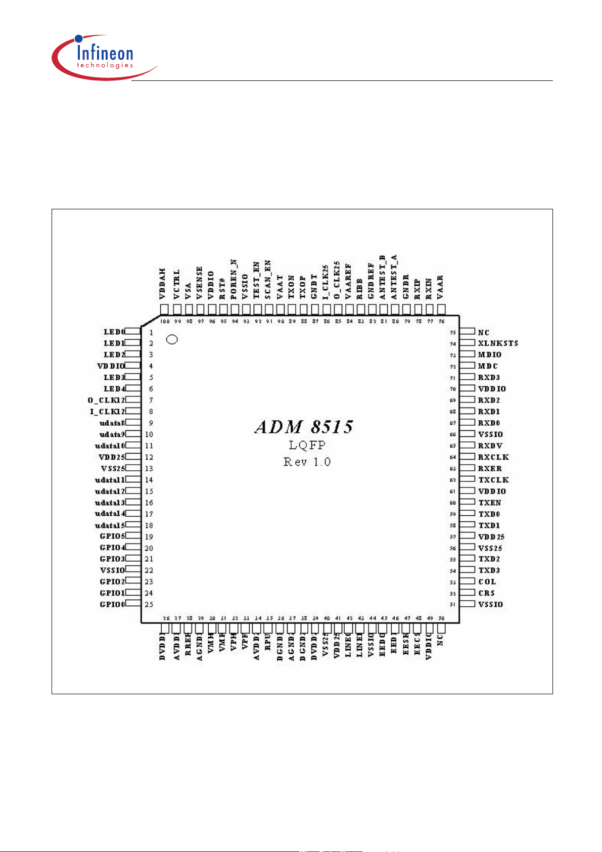
2.1 Pin Diagram
Pin Diagram of ADM8515/X.
Interface Description
Figure 2 Pin Diagram
Data Sheet 12 Rev. 1.21, 2005-11-08

ADM8515/X
2.2 Pin Description by Function
ADM8515/X pins are categorized into one of the following groups:
• Host Interface
• MII Interface
• Physical Layer Interface
• LED Display Mode
• EEPROM Interface
• Regulator Pins
• Power Pins
• Miscellaneous
Table 2 Abbreviations for Pin Type
Abbreviations Description
I Standard input-only pin. Digital levels.
O Output. Digital levels.
I/O I/O is a bidirectional input/output signal.
AI Input. Analog levels.
AO Output. Analog levels.
AI/O Input or Output. Analog levels.
PWR Power
GND Ground
MCL Must be connected to Low (JEDEC Standard)
MCH Must be connected to High (JEDEC Standard)
NU Not Usable (JEDEC Standard)
NC Not Connected (JEDEC Standard)
Interface Description
Table 3 Abbreviations for Buffer Type
Abbreviations Description
Z High impedance
PU1 Pull up, 10 kΩ
PD1 Pull down, 10 kΩ
PD2 Pull down, 20 kΩ
TS Tristate capability: The corresponding pin has 3 operational states: Low, high and high-
impedance.
OD Open Drain. The corresponding pin has 2 operational states, active low and tristate, and
allows multiple devices to share as a wire-OR. An external pull-up is required to sustain the
inactive state until another agent drives it, and must be provided by the central resource.
OC Open Collector
PP Push-Pull. The corresponding pin has 2 operational states: Active-low and active-high
(identical to output with no type attribute).
OD/PP Open-Drain or Push-Pull. The corresponding pin can be configured either as an output with
the OD attribute or as an output with the PP attribute.
ST Schmitt-Trigger characteristics
TTL TTL characteristics
Data Sheet 13 Rev. 1.21, 2005-11-08

ADM8515/X
Interface Description
2.2.1 Host Interface
Table 4 Host Interface
Pin or Ball
No.
8 I_CLK12 I Input Clock
7 O_CLK12 O Output for Crystal
95 RST# I External Hardware Reset Input
94 POREN_N I Internal Power on Reset Logic Enable
32 VPH I/O USB D + Port for High Speed
30 VMH I/O USB D - Port for High Speed
33 VPF I/O USB D + Port for Full Speed
31 VMF I/O USB D - Port for Full Speed
28 RREF Pull Down with 510 Ohm Precise Resistor ( ± 1%)
35 RPU Pull up with a 1.5 k Ohm Resistor
42 LINE0 O USB Line State
43 LINE1
Name Pin
Type
Buffer
Type
Function
12 MHz clock input from crystal or oscillator.
Schmitt trigger, internal pull high.
Default is enable and internal pull-low. When external
hardware reset is used, this pin should be connected to Vcc
via 4.7 kΩ resistor.
They directly reflect the current state of the DP (LINE1) and
DM (LINE0) signals, see Table 5
Table 5 DM and DP Signals
DM DP Description
000: SE0
0 1 1: “J” State
1 0 2: “K” State
113: SE1
Data Sheet 14 Rev. 1.21, 2005-11-08

ADM8515/X
Interface Description
2.2.2 MII Interface
Note: Program ADM8515/X as MAC-only mode, set register 81H[4:2] = 001B and register 01H bit 2 = 0
Table 6 MII Interface
Pin or Ball
No.
53 COL I Collision Detected
52 CRS I Carrier Sense
72 MDC O Management Data Clock
73 MDIO I/O Management Data I/O
64 RXCLK I Receive Clock
71 RXD3 I Receive Data
69 RXD2
68 RXD1
67 RXD0
65 RXDV I Receive Data Valid
63 RXER I Receive Error
62 TXCLK I Transmit Clock
Name Pin
Type
Buffer
Type
Function
This signal is asserted high asynchronously by the external
physical unit upon detection of a collision on the medium. It
will remain asserted as long as the collision condition
persists.
This signal is asserted high asynchronously by the external
physical unit upon detection of a non-idle medium.
Clock signal with a maximum rate of 2.5 MHz used to
transfer management data for the external PMD on the
MDIO pin.
Bi-directional signal used to transfer management
information for the external PMD. Requires a 1.5 kΩ pull-up
resistor if external PHY is used.
A continuous clock that is recovered from the incoming
data. During 100 Mbit/s operation, RXCLK is 25 MHz.
During 10 Mbit/s, this is 2.5 MHz.
This is a group of 4 data signals aligned on nibble boundary
which are driven synchronous to the RXCLK by the external
physical unit. RXD[3] is the most significant bit and RXD[0]
is the least significant bit.
This indicates that the external physical unit is presenting
recovered and decoded nibbles on the RXD[3:0] and that
RXCLK is synchronous to the recovered data
This signal is asserted high synchronously by the external
physical unit whenever it detects a media error and RXDV
is asserted. If not used, it should be grounded, e.g. isolate
internal PHY and use external PHY.
A continuous clock that gets its source by the physical
layer. During 100 Mbit/s operation, this clock is 25 MHz.
During 10 Mbit/s operation, this clock is 2.5 MHz.
Data Sheet 15 Rev. 1.21, 2005-11-08

ADM8515/X
Table 6 MII Interface (cont’d)
Pin or Ball
No.
54 TXD3 O Transmit Data
55 TXD2
58 TXD1
59 TXD0
60 TXEN O Transmit Enable
74 XLNKSTS I Link Status Indication
Name Pin
Type
Buffer
Type
Function
This is a group of 4 data signals which are driven
synchronously to the TXCLK for transmission to the
external physical unit. TXD[3] is the most significant bit and
TXD[0] is the least significant bit.
This signal is synchronous to TXCLK and provides precise
framing for data carried on TXD[3:0]. It is asserted when
TX[3:0] contains valid data to be transmitted. Requires
external pull-down resistor 4.7 kΩ if external PHY is used.
External PHY reports link status information to system and
level change trigger. Connect to external PHY’s link status
report pin or pull-down to low if not used.
2.2.3 Physical Layer Interface
Interface Description
Table 7 Physical Layer Interface
Pin or Ball
No.
85 O_CLK25 O Crystal Out
86 I_CLK25 I Crystal In
78 RXIP I Receives Inputs
77 RXIN
88 TXOP O Transmits Outputs
89 TXON
83 RIBB I Reference Bias Resistor
80 ANTEST_A O PHY Test Pins
81 ANTEST_B
Name Pin
Type
Buffer
Type
Function
25 MHz
25 MHz
The differential receives inputs of 100BASE-TX or
10BASE-T, these pins directly input from Magnetic.
The differential transmits outputs of 100BASE-TX or
10BASE-T, these pins directly output to Magnetic.
To be tied to an external 10.0 kΩ (1%) resistor which should
be connected to the analog ground at the other end.
Data Sheet 16 Rev. 1.21, 2005-11-08

ADM8515/X
Interface Description
2.2.4 LED Display Mode
Table 8 LED Display Mode
Pin or Ball
No.
1LED0O Function of LED0
2LED1O Function of LED1
3LED2O Function of LED2
5LED3O LED Display for USB Full
6LED4O LED Display for USB High
The LED interface is EEPROM programmable, 2 EEPROM control bits, Address OB [7:6] in EEPROM are used
to select the LED display mode.
Name Pin
Type
Buffer
Type
Function
Function of LED0 is described below.
Function of LED1 is described below.
Function of LED2 is described below.
LED display for USB full speed rate link, active high.
LED display for USB high speed rate link, active high.
Notes
1. EEPROM 0B[7:6] = 00
B
LED0: 100 Mbit/s (on, drive '0') or 10 Mbit/s (off, drive '1')
LED1: Link (keeps on when link on) or Activity (Flash with 10 Hz when ADM8515/X is receiving or transmitting
without collision)
LED2: Full duplex (keeps on when in full duplex mode) or Collision (flash with 20 Hz when collision occurred
in half duplex mode)
2. EEPROM 0B[7:6] = 01
B
LED0: Activity (Flash with 10 Hz when ADM8515/X is receiving or transmitting without collision)
LED1: Link 10 (keeps on when link on 10 Mbit/s)
LED2: Link 100 (keeps on when link on 100 Mbit/s)
3. EEPROM 0B[7:6] = 10
B
LED0: 100 Mbit/s (on, drive '0') or 10 Mbit/s (off, drive '1')
LED1: Activity (Flash with 10 Hz when ADM8515/X is receiving or transmitting without collision)
LED2: Link (keeps on when link on)
4. EEPROM 0B[7:6] = 11
B
LED0: Link 10 (LED on when link on 10Mbit/s) and Activity (Flash with 10Hz when ADM8515/X is receiving or
transmitting without collision)LED1: Link 100 (LED on when link on 100Mbit/s) and Activity (Flash with 10Hz
when ADM8515/X is receiving or transmitting without collision) LED2: Full duplex (keeps on when in full duplex
mode)
Data Sheet 17 Rev. 1.21, 2005-11-08

ADM8515/X
2.2.5 EEPROM Interface
Table 9 EEPROM Interface
Pin or Ball
No.
48 EECS O EEPROM Chip Select
46 EEDI O EEPROM Data In
45 EEDO I EEPROM Data Out
47 EESK O EEPROM Clock
Name Pin
Type
Buffer
Type
Function
This pin enables the EEPROM during loading of the
Ethernet configuration data.
ADM8515/X will use this pin to serially write opcodes,
addresses and data into the serial EEPROM.
ADM8515/X will read the contents of the EEPROM serially
through this pin.
After reset, ADM8515/X will auto-load the contents of the
EEPROM by using EESK, EEDO, and EEDI. This pin
provides the clock for the EEPROM device.
Interface Description
2.2.6 Regulator Pins
Table 10 Regulator Pins
Pin or Ball
No.
100 VDDAH P Chip Regulator
98 VSA P Ground for Regulator
99 VCTRL I/O Regulator Control Pin
97 VSENSE I 2.5 V Voltage Sense Input
Note: ADM8515/X is a dual power device, it needs both 3.3 V and 2.5 V power supply. Inside the chip, there is an
embedded 3.3 V to 2.5 V power regulator that can generate the needed 2.5 V power to supply the chip. The
reference schematics design is shown in Figure 3
Name Pin
Type
Buffer
Type
Function
3.3 V power supply for on chip regulator.
Data Sheet 18 Rev. 1.21, 2005-11-08

ADM8515/X
Figure 3 Reference Design
2.2.7 Power Pins
Table 11 Power Pins
Pin or Ball
No.
12, 41, 57 VDD25 P 2.5 V Power Supply for Core
13, 40, 56 VSS25 P Ground for VDD25
4, 49, 61, 70, 96VDDIO P 3.3 V Power Supply for I/O
Name Pin
Type
Buffer
Type
Function
Interface Description
22, 44, 51,
66, 93
26 DVDD1 P 2.5 V Digital Power Supply
39 DVDD2
36 DGND1 P Digital Ground
38 DGND2
27 AVDD1 P 3.3 V Analog Power Supply
34 AVDD2
29 AGND1 P Analog Ground
37 AGND2
90 VAAT P 3.3 V Power Supply for Transmitter
87 GNDT P Ground for VAAT
76 VAAR P 3.3 V Power Supply for Receiver
79 GNDR P Ground for VAAR
84 VAAREF P 3.3 V Power Supply for PHY
82 GNDREF P Ground for VAAREF
VSSIO P Ground for VDDIO
Data Sheet 19 Rev. 1.21, 2005-11-08

ADM8515/X
2.2.8 Miscellaneous
Table 12 Miscellaneous
Pin or Ball
No.
19 GPIO5 I/O General Purpose Input/Output Pins
20 GPIO4
21 GPIO3
23 GPIO2
24 GPIO1
25 GPIO0
92, 91 TEST 1 I Test Pins
9, 10, 11, 14,
15, 16, 17,
18
Name Pin
Type
TEST2 I/O Test Pins
Buffer
Type
Function
These pins are used as general purpose Input/Output pins.
These pins are internal pull-low.
Interface Description
Data Sheet 20 Rev. 1.21, 2005-11-08

ADM8515/X
Function Description
3 Function Description
3.1 USB Interface
USB is a straightforward solution when you want to use a computer for communication with devices outside the
computer. The interface is suitable for one-of-kind and small-scale designs as well as mass-produced, standard
peripheral. The benefits of USB are easy to use and easy to apply, fast and reliable data transfers, flexibility, cost,
and power conservation.
3.1.1 PIE
PIE (Parallel Interface Engine) is to control USB communications and check USB protocol, then transfer protocol
to EP decoder. The PIE and USB transceivers, which provide the hardware interface to the USB cable, together
comprise the USB engine.
3.1.2 EP Decoder
The detail description is in Section 4.5 USB Command.
3.2 MAC Controller
3.2.1 MII
The Media Independent Interface (MII) is an 18 wire MAC/PHY interface described in 802.3u. The purpose of the
interface is to allow MAC layer devices to attach to a variety of Physical Layer devices through a common
interface. MII operates at 100 Mbit/s or 10 Mbit/s, dependant on the speed of the Physical Layer. With clocks
running at either 25 MHz or 2.5 MHz, 4 bit data is clocked between the MAC and PHY, synchronous with Enable
and Error signals.
On receipt of valid data from the wire interface, RX_DV will go active signaling to the MAC that the valid data will
be presented on the RXD[3:0] pins at the speed of the RX_CLK.
On transmission of data from the MAC, TX_EN is presented to the PHY indicating the presence of valid data on
TXD[3:0]. TXD[3:0] are sampled by the PHY synchronous to TX_CLK during the time that TX_EN is valid.
3.2.2 Adaptive Equalizer
The amplitude and phase distortion from a cable causes inter-symbol interference (ISI) which makes clock and
data recovery difficult. The adaptive equalizer is designed to closely match the inverse transfer function of the
twisted-pairs cable. The equalizer has the ability to change its equalizer frequency response according to the cable
length. The equalizer will tune itself automatically for any cable, compensating for the amplitude and phase
distortion introduced by the cable.
3.2.3 Jabber and SQE
After the MAC transmitter exceeds the jabber timer, the transmit and loop back functions will be disabled and COL
signal gets asserted. After TX_EN goes low for more than 500 ms, the TP transmitter will reactivate and COL gets
de-asserted. Setting Jabber Disable will disable the jabber function.
When the SQE test is enabled, a COL pulse is asserted after each transmitted packet. SQE is enabled in
10Base-T by default.
Data Sheet 21 Rev. 1.21, 2005-11-08

ADM8515/X
Function Description
3.2.4 Auto Polarity
Certain cable plants have crossed wiring on the twisted pairs; the reversal of TXIN and TXIP. Under normal
circumstances this would cause the receive circuitry to reject all data. When the Auto Polarity Disable bit is cleared,
the PHY has the ability to detect the fact that either 8 Normal Link Pulses (NLP) or a burst of FLPs are inverted
and automatically reverse the receiver’s polarity. The polarity state is stored in the Reverse Polarity bit.
3.2.5 Auto-Negotiation
It provides a linked device with the capability to detect the abilities (modes of operations) supported by the device
at the other end of the link, determine common abilities, and configure for joint operation. Auto-Negotiation is
performed out-of-band using a pulse code sequence that is compatible with the 10BASE-T link integrity test
sequence.
3.2.6 Baseline Wander Compensation
The 100BASE-TX data stream is not always DC balanced. The transformer blocks the DC components of the
incoming signal, thus the DC offset of the differential receive inputs can drift. The shifting of the signal level,
coupled with non-zero rise and fall times of the serial stream can cause pulse-width distortion. This creates jitter
and possible increase in the bit error rates. Therefore, a DC restoration circuit is needed to compensate for the
attenuation of the DC component. Unlike the traditional implementation, the circuit does not need the feedback
information from the slicer or the clock recovery circuit. The design simplifies the circuit design. In 10BASE-T, the
baseline wander correction circuit is not required.
3.3 FIFO Controller
3.3.1 FIFO Controller in Receive Path
• Store received Ethernet packets to SRAM (internal 24 Kbyte) and total 16 packets can be stored to SRAM. If
more than 16 packets are received or total packet size is more than 24 Kbytes, the subsequent coming
Ethernet packet will be discarded.
• FIFO controller will load data from SRAM to internal RX FIFO then inform EP Decoder that 512-byte data or a
packet is ready in RX FIFO. Before FIFO controller informs about this, any USB access to bulk IN endpoint will
return NAK. This is to maintain the data transfer on USB bus via bulk IN transfer is continuous, thus a 512-byte
internal RX FIFO is needed.
• If an Ethernet packet is being received and loading into SRAM while FIFO Controller is moving data from
SRAM to internal RX FIFO, writing the Ethernet packet to SRAM will get the higher priority.
3.3.2 FIFO Controller in Transmit Path
• Store each individual USB packet to internal TX FIFO. When EP decoder informs end of packet, a complete
Ethernet packet is stored in TX FIFO. FIFO Controller then informs MAC to transmit this packet.
• Total 4 Ethernet packets can be stored in TX FIFO. If all 4 Ethernet packets are stored in TX FIFO or total
packet size is more than 2 Kbytes, FIFO Controller will inform EP Decoder that TX FIFO is full and EP Decoder
will return NAK if accessing to bulk OUT endpoint is invoked. Thus additional USB packet won’t be written into
TX FIFO until TX FIFO has free space.
3.4 TX FIFO and RX FIFO
RX FIFO is a one-port 512 byte FIFO and TX FIFO is a two-port 2 Kbyte FIFO
Data Sheet 22 Rev. 1.21, 2005-11-08

ADM8515/X
Function Description
3.5 10/100M Ethernet PHY
The Ethernet PHY is compliant to IEEE 802.3u 100BASE-TX and IEEE802.3 10BASE-T. It provides the whole
physical layer functions for both 10M and 100M Ethernet speed.
3.6 USB Device Endpoint Operation
3.6.1 Endpoint 0
Endpoint 0 is in charge of response to standard USB commands and vendor specific commands. Internal register
settings are also via this Endpoint 0. The response to each command is described in “USB Commands”.
3.6.2 Endpoint 1 Bulk IN
Endpoint 1 is in charge of sending the received Ethernet packet to USB host. An Ethernet packet will be split to
multiple 512 bytes USB packets on USB. The end of the Ethernet packet is indicated by less then 512 byte or 0
length data transfer in this pipe. The Ethernet received status is optionally reported at the end of the packet.
While accessing to this endpoint, if RXFIFO is either full or any packet is inside, the data in RXFIFO is returned in
USB data stage. If ACK is received from USB host, data in RXFIFO is flushed. If no response or NAK is received
from USB host, the content in RXFIFO will be re-transmitted. If RXFIFO isn’t ready for transmission, NAK is
returned to USB host.
Figure 4 Packet Form when Receive
The Received Status is Reported as Follows:
Table 13 USB Received Status
Offset Bit Field Description
Offset0 7-0 rx_bytecnt_lo The received byte count[7:0].
Offset1 3-0 rx_bytecnt_hi The received byte count[11:8].
7-4 reserved
Offset2 0 multicast_frame Indicates received multicast frame.
1 long_pkt Indicates received packet length > 1518 bytes.
2 runt_pkt Indicates received packet length < 64 bytes.
3 crc_err Indicates CRC check error.
4 dribble_bit Indicates packet length is not integer multiple of 8-
bit.
7-5 reserved
Offset3 7-0 reserved
Data Sheet 23 Rev. 1.21, 2005-11-08

ADM8515/X
Function Description
3.6.3 Endpoint 2 Bulk OUT
Endpoint 2 is in charge of sending the USB packet to Ethernet. An Ethernet packet is concatenated by multiple
512 bytes USB packets on USB. The first two bytes in every first concatenated USB packet indicate the length of
the Ethernet packet. The end of the Ethernet packet is indicated by less then 512-byte or 0 length data transfer in
this pipe. The Ethernet transmit status is reported in transmit status register.
When access to this endpoint, data in USB data stage are transferred to TXFIFO, if TXFIFO is free and ACK is
returned. If TXFIFO isn’t free, NAK is returned.
Table 14 USB Packet Format
Field 1st Byte in 1st USB Packet 2nd Byte in 1st USB Packet The Following Packets
Content len[7:0]: Low byte Ethernet
packet length
{reserved[4:0], len[10:8]} Ethernet packet
Figure 5 Packet Form when Transmit
3.6.4 Endpoint 3 Interrupt IN
Endpoint 3 is in charge of returning the current Ethernet transfer status every polling interval. When access to this
endpoint, 8 bytes data is returned to USB host. The 8-byte packet contains the following in the tables below:
Table 15 Interrupt Packet Form
Offset0 Offset1 Offset2 Offset3 Offset4
tx_status(Reg2B
Table 16 Interrupt Packet Form
Offset5 Offset6(1B) Offset7(1B)
wakeup_status(Reg7A
) tx_status(Reg2CH) rx_status(Reg2DH) rx_lostpkt(Reg2EH) rx_lostpkt(Reg2FH)
H
) Packet number in RX FIFO
H
(Reg82
)
H
7’b00, length error
Data Sheet 24 Rev. 1.21, 2005-11-08

ADM8515/X
Registers DescriptionSystem Registers
4 Registers Description
4.1 System Registers
Table 17 Registers Address Space
Module Base Address End Address Note
0000 0000
H
Table 18 Registers Overview
Register Short Name Register Long Name Offset Address Page Number
EC0 Ethernet Control 0 00
EC1 Ethernet Control 1 01
EC2 Ethernet Control 2 02
Res0 Reserved 0 03
Res1 Reserved 1 04
Res2 Reserved 2 05
Res3 Reserved 3 06
Res4 Reserved 4 07
MA0 Multicast Address 0 08
MA1 Multicast Address 1 09
MA2 Multicast Address 2 0A
MA3 Multicast Address 3 0B
MA4 Multicast Address 4 0C
MA5 Multicast Address 5 0D
MA6 Multicast Address 6 0E
MA7 Multicast Address 7 0F
EID0 Ethernet ID 0 10
EID1 Ethernet ID 1 11
EID2 Ethernet ID 2 12
EID3 Ethernet ID 3 13
EID4 Ethernet ID 4 14
EID5 Ethernet ID 5 15
Res5 Reserved 5 16
Res6 Reserved 6 17
PT Pause Timer 18
Res7 Reserved 7 19
RPNBFC Receive Packet Number Based Flow Control 1A
ORFBFC Occupied Receive FIFO Based Flow Control 1B
EP1C EP1 Control 1C
Res8 Reserved 8 1D
0000 0082
H
H
H
H
H
H
H
H
H
H
H
H
H
H
H
H
H
H
H
H
H
H
H
H
H
H
H
H
H
H
H
28
29
30
31
31
31
31
31
32
32
33
33
34
34
35
35
36
36
37
37
38
38
31
31
39
31
39
40
40
31
Data Sheet 25 Rev. 1.21, 2005-11-08

ADM8515/X
Registers DescriptionSystem Registers
Table 18 Registers Overview (cont’d)
Register Short Name Register Long Name Offset Address Page Number
BIST BIST 1E
Res9 Reserved 9 1F
EEPROMO EEPROM Offset 20
EEPROMDL EEPROM Data Low 21
EEPROMDH EEPROM Data High 22
EEPROMAC EEPROM Access Control 23
Res10 Reserved 10 24
PHYA PHY Address 25
PHYDL PHY Data Low 26
PHYDH PHY Data High 27
PHYAC PHY Access Control 28
Res11 Reserved 11 29
USBBS USB Bus Status 2A
TS1 Transmit Status 1 2B
TS2 Transmit Status 2 2C
RS Receive Status 2D
RLPCH Receive Lost Packet Count High 2E
RLPCL Receive Lost Packet Count Low 2F
WUF0M_0 Wakeup Frame 0 Mask 30
WUF0M_1 Wakeup Frame 0 Mask 1 31
... ... ...
WUF0M_xx Wakeup Frame 0 Mask xx 3F
WUF0O_0 Wakeup Frame 0 Offset 40
WUF0CRCL Wakeup Frame 0 CRC Low 41
WUF0CRCH Wakeup Frame 0 CRC High 42
Res12 Reserved 12 43
Res13 Reserved 13 44
Res14 Reserved 14 45
Res15 Reserved 15 46
Res16 Reserved 16 47
WUF1M_0 Wakeup Frame 1 Mask 48
WUF1M_1 Wakeup Frame 1 Mask 1 49
... ... ...
WUF1M_xx Wakeup Frame 1 Mask xx 57
WUF1O Wakeup Frame 1 Offset 58
WUF1CRCL Wakeup Frame 1 CRC Low 59
WUF1CRCH Wakeup Frame 1 CRC High 5A
Res17 Reserved 17 5B
Res18 Reserved 18 5C
Res19 Reserved 19 5D
Res 20 Reserved 20 5E
H
H
H
H
H
H
H
H
H
H
H
H
H
H
H
H
H
H
H
H
H
H
H
H
H
H
H
H
H
H
H
H
H
H
H
H
H
H
H
H
H
40
31
41
41
42
43
31
43
44
44
45
31
45
45
47
47
48
48
48
49
49
49
49
50
50
31
31
31
31
31
51
51
51
51
51
52
52
31
31
31
31
Data Sheet 26 Rev. 1.21, 2005-11-08

ADM8515/X
Registers DescriptionSystem Registers
Table 18 Registers Overview (cont’d)
Register Short Name Register Long Name Offset Address Page Number
Res 21 Reserved 21 5F
WUF2M Wakeup Frame 2 Mask 60
WUF2M_1 Wakeup Frame 2 Mask 1 61
... ... ...
WUF2M_xx Wakeup Frame 2 Mask xx 6F
WUF2O Wakeup Frame 2 Offset 70
WUF2CRCL Wakeup Frame 2 CRC Low 71
WUF2CRCH Wakeup Frame 2 CRC High 72
Res 22 Reserved 22 73
Res 23 Reserved 23 74
Res 24 Reserved 24 75
Res 25 Reserved 25 76
Res 26 Reserved 26 77
WUC Wakeup Control 78
Res 27 Reserved 27 79
WUS Wakeup Status 7A
IPHYC Internal PHY Control 7B
GPIO54C GPIO[5:4] Control 7C
Res 28 Reserved 28 7D
GPIO10C GPIO[1:0] Control 7E
GPIO32C GPIO[3:2] Control 7F
Test TEST 80
TM Test Mode 81
RPN Receive Packet Number 82
Res 29 Reserved 29 83
... ... ...
Res xx Reserved xx FF
H
H
H
H
H
H
H
H
H
H
H
H
H
H
H
H
H
H
H
H
H
H
H
H
H
H
H
31
53
53
53
53
53
54
54
31
31
31
31
32
55
32
56
56
57
32
58
59
60
60
61
32
32
32
The register is addressed wordwise.
Table 19 Register Access Types
Mode Symbol Description HW Description SW
read/write rw Register is used as input for the HW Register is readable and writable by SW
read r Register is written by HW (register
between input and output -> one cycle
delay)
Value written by software is ignored by
hardware; that is, software may write any
value to this field without affecting hardware
behavior (= Target for development.)
Read only ro Register is set by HW (register between
SW can only read this register
input and output -> one cycle delay)
Read virtual rv Physically, there is no new register, the
SW can only read this register
input of the signal is connected directly
to the address multiplexer.
Data Sheet 27 Rev. 1.21, 2005-11-08

ADM8515/X
Registers DescriptionSystem Registers
Table 19 Register Access Types (cont’d)
Mode Symbol Description HW Description SW
Latch high,
self clearing
Latch low,
self clearing
Latch high,
mask clearing
Latch low,
mask clearing
Interrupt high,
self clearing
Interrupt low,
self clearing
Interrupt high,
mask clearing
Interrupt low,
mask clearing
lhsc Latch high signal at high level, clear on
read
llsc Latch high signal at low-level, clear on
read
lhmk Latch high signal at high level, register
cleared with written mask
llmk Latch high signal at low-level, register
cleared on read
ihsc Differentiate the input signal (low-
>high) register cleared on read
ilsc Differentiate the input signal (high-
>low) register cleared on read
ihmk Differentiate the input signal (high-
>low) register cleared with written mask
ilmk Differentiate the input signal (low-
>high) register cleared with written
SW can read the register
SW can read the register
SW can read the register, with write mask
the register can be cleared (1 clears)
SW can read the register, with write mask
the register can be cleared (1 clears)
SW can read the register
SW can read the register
SW can read the register, with write mask
the register can be cleared
SW can read the register, with write mask
the register can be cleared
mask
Interrupt enable
register
latch_on_reset lor rw register, value is latched after first
ien Enables the interrupt source for
interrupt generation
SW can read and write this register
Register is readable and writable by SW
clock cycle after reset
Read/write
self clearing
rwsc Register is used as input for the hw, the
register will be cleared due to a HW
mechanism.
Writing to the register generates a strobe
signal for the HW (1 pdi clock cycle)
Register is readable and writable by SW.
Table 20 Registers Clock Domains
Clock Short Name Description
4.1.1 Registers
Ethernet Control 0
EC0 Offset Reset Value
Ethernet Control 0 00
H
7;(
UZ
5;(
UZ
5;)&(
UZ
:2(
UZ
5;6$
UZ
6%2
UZ
5;0$
UZ
09
5;&6
UZ
H
Data Sheet 28 Rev. 1.21, 2005-11-08

ADM8515/X
Registers DescriptionSystem Registers
Field Bits Type Description
TXE 7 rw Ethernet Transmission Enable
1
tx_en, Enable
B
RXE 6 rw Ethernet Receive Enable
1
rx_en, Enable
B
RXFCE 5 rw Receive Pause Frame Enable
1
rx_flowctl_en, Enable
B
WOE 4 rw Wake-on-LAN Mode Enable
1
wakeon_en, Enable
B
RXSA 3 rw Status Append at the End of Received Packet
1
rxstatus_append, Enable
B
SBO 2 rw Stop Back Off
0
CNOT, Back-off counter isn’t affected by carrier
B
1
CST, Back-off counter stop when carrier is active and resume when
B
carrier drop
RXMA 1 rw Receive All Multicast Packets
1
RALL, Receives all multicast packets
B
RXCS 0 rw Include CRC in Receive Packet
1
ICRC, Includes CRC in receive packet
B
Ethernet Control 1
EC1 Offset Reset Value
Ethernet Control 1 01
H
00
5HV
)'
UZ
0
UZ
50
UZ
5HV
Field Bits Type Description
FD 5 rw Full Dublex
0
HDM, Half-duplex mode
B
1
FDM, Full-duplex mode
B
10M 4 rw 10mode
0
10Base, 10Base-T mode
B
1
100Base, 100Base-T mode
B
RM 3 rw Reset MAC
After write 1, HW will clear this bit after MAC reset.
H
Data Sheet 29 Rev. 1.21, 2005-11-08

ADM8515/X
Registers DescriptionSystem Registers
Ethernet Control 2
EC2 Offset Reset Value
Ethernet Control 2 02
H
40
0(3/
UZ
531&
UZ
/((356
UZ
((35:
UZ
/%
UZ
3520
UZ
5;%3
UZ
(35&
UZ
Field Bits Type Description
MEPL 7 rw Max Ethernet Packet Length
0
1528B, 1528 bytes
B
1
1638B, 1638 bytes, Default is 0
B
RPNC 6 rw Receive Packet Number Control
This bit controls the clear operation of Register 82
(Receive packet
H
number register)
0
NRC, No read clear
B
1
RC, Read clear
B
LEEPRS 5 rw Load EEPROM Start
When this bit is written with 1, HW will start to load EEPROM.
EEPRW 4 rw EEPROM Write Enable/disable
0
WEDC, EEPROM write enable/disable command
B
1
WC, EEPROM write command
B
LB 3 rw Loop Back
Enable MAC loop back mode.
PROM 2 rw Promiscuous
0
RPP, Receives packets which pass the address filter
B
1
RAP, Receives any packets
B
RXBP 1 rw Receive Bad Packets
0
FABP, Filter all bad packet
B
RBPP, Receives bad packets which pass the address filter
1
B
EP3RC 0 rw EP3 Read Cleared
0
AEP3, Access EP3, no effect to those registers.
B
1
OEP3, Once EP3 is accessed, those registers (2B-2F, 7A) will be
B
cleared.
H
Data Sheet 30 Rev. 1.21, 2005-11-08

ADM8515/X
Registers DescriptionSystem Registers
Reserved 0
Res0 Offset Reset Value
Reserved 0 03
H
00
5HV
UR
Field Bits Type Description
Res 7:0 ro Reserved
Similar Registers
Table 21 Reserved Registers
Register Short Name Register Long Name Offset Address Page Number
Res1 Reserved 1 04
Res2 Reserved 2 05
Res3 Reserved 3 06
Res4 Reserved 4 07
Res5 Reserved 5 16
Res6 Reserved 6 17
Res7 Reserved 7 19
Res8 Reserved 8 1D
Res9 Reserved 9 1F
Res10 Reserved 10 24
Res11 Reserved 11 29
Res12 Reserved 12 43
Res13 Reserved 13 44
Res14 Reserved 14 45
Res15 Reserved 15 46
Res16 Reserved 16 47
Res17 Reserved 17 5B
Res18 Reserved 18 5C
Res19 Reserved 19 5D
Res 20 Reserved 20 5E
Res 21 Reserved 21 5F
Res 22 Reserved 22 73
Res 23 Reserved 23 74
Res 24 Reserved 24 75
Res 25 Reserved 25 76
H
H
H
H
H
H
H
H
H
H
H
H
H
H
H
H
H
H
H
H
H
H
H
H
H
H
Data Sheet 31 Rev. 1.21, 2005-11-08

ADM8515/X
Registers DescriptionSystem Registers
Table 21 Reserved Registers
Register Short Name Register Long Name Offset Address Page Number
Res 26 Reserved 26 77
Res 27 Reserved 27 79
Res 28 Reserved 28 7D
Res 29 Reserved 29 83
... ... ...
Res xx Reserved xx FF
H
H
H
H
H
H
Multicast Address 0
MA0 Offset Reset Value
Multicast Address 0 08
H
00
0$%
H
UZ
Field Bits Type Description
MAB0 7:0 rw Multicast 0
Multicast address byte [7:0]
Multicast Address 1
MA1 Offset Reset Value
Multicast Address 1 09
H
00
0$%
UZ
Field Bits Type Description
MAB1 7:0 rw Multicast 1
Multicast address byte [15:8]
H
Data Sheet 32 Rev. 1.21, 2005-11-08

ADM8515/X
Registers DescriptionSystem Registers
Multicast Address 2
MA2 Offset Reset Value
Multicast Address 2 0A
H
00
0$%
UZ
Field Bits Type Description
MAB2 7:0 rw Multicast 2
Multicast address byte [23:16]
Multicast Address 3
H
MA3 Offset Reset Value
Multicast Address 3 0B
H
00
0$%
UZ
Field Bits Type Description
MAB3 7:0 rw Multicast 3
Multicast address byte [31:24]
H
Data Sheet 33 Rev. 1.21, 2005-11-08

ADM8515/X
Registers DescriptionSystem Registers
Multicast Address 4
MA4 Offset Reset Value
Multicast Address 4 0C
H
00
0$%
UZ
Field Bits Type Description
MAB4 7:0 rw Multicast 4
Multicast address byte [39:32]
Multicast Address 5
H
MA5 Offset Reset Value
Multicast Address 5 0D
H
00
0$%
UZ
Field Bits Type Description
MAB5 7:0 rw Multicast 5
Multicast address byte [47:40]
H
Data Sheet 34 Rev. 1.21, 2005-11-08

ADM8515/X
Registers DescriptionSystem Registers
Multicast Address 6
MA6 Offset Reset Value
Multicast Address 6 0E
H
00
0$%
UZ
Field Bits Type Description
MAB6 7:0 rw Multicast 6
Multicast address byte [55:48]
Multicast Address 7
H
MA7 Offset Reset Value
Multicast Address 7 0F
H
00
0$%
UZ
Field Bits Type Description
MAB7 7:0 rw Multicast 7
Multicast address byte [63:56]
H
Data Sheet 35 Rev. 1.21, 2005-11-08

ADM8515/X
Registers DescriptionSystem Registers
Ethernet ID 0
EID0 Offset Reset Value
Ethernet ID 0 10
H
00
(,'
UZ
Field Bits Type Description
EID0 7:0 rw Ethernet ID 0
The 1st byte of Ethernet ID is automatically loaded from EEPROM after
HW reset.
Ethernet ID 1
H
EID1 Offset Reset Value
Ethernet ID 1 11
H
00
(,'
UZ
Field Bits Type Description
EID1 7:0 rw Ethernet ID 1
The 2nd byte of Ethernet ID.
H
Data Sheet 36 Rev. 1.21, 2005-11-08

ADM8515/X
Registers DescriptionSystem Registers
Ethernet ID 2
EID2 Offset Reset Value
Ethernet ID 2 12
H
00
(,'
UZ
Field Bits Type Description
EID2 7:0 rw Ethernet ID 2
The 3rd byte of Ethernet ID.
Ethernet ID 3
H
EID3 Offset Reset Value
Ethernet ID 3 13
H
00
(,'
UZ
Field Bits Type Description
EID3 7:0 rw Ethernet ID 3
The 4th byte of Ethernet ID.
H
Data Sheet 37 Rev. 1.21, 2005-11-08

ADM8515/X
Registers DescriptionSystem Registers
Ethernet ID 4
EID4 Offset Reset Value
Ethernet ID 4 14
H
00
(,'
UZ
Field Bits Type Description
EID4 7:0 rw Ethernet ID 4
The 5th byte of Ethernet ID.
Ethernet ID 5
H
EID5 Offset Reset Value
Ethernet ID 5 15
H
00
(,'
UZ
Field Bits Type Description
EID5 7:0 rw Ethernet ID 5
The 6th byte of Ethernet ID.
H
Data Sheet 38 Rev. 1.21, 2005-11-08

ADM8515/X
Registers DescriptionSystem Registers
Pause Timer
PT Offset Reset Value
Pause Timer 18
H
00
37
UZ
Field Bits Type Description
PT 7:0 rw Pause Timer
The [11:4] of pause time in the PAUSE frame.
Receive Packet Number Based Flow Control
H
RPNBFC Offset Reset Value
Receive Packet Number Based Flow Control 1A
H
00
5HV
31
UZ
)&3
UZ
Field Bits Type Description
PN 6:1 rw Packet Number
This field specifies the threshold for transmitting the PAUSE frame. As
the received packet number is more than or equal to this field, the PAUSE
frame is sent automatically by HW.
FCP 0 rw Flow Control Packet
1
RPN, Enable pause frame transmission bases on receive packet
B
number
H
Data Sheet 39 Rev. 1.21, 2005-11-08

ADM8515/X
Registers DescriptionSystem Registers
Occupied Receive FIFO Based Flow Control
ORFBFC Offset Reset Value
Occupied Receive FIFO Based Flow Control 1B
H
00
5HV
5;6
UZ
)&5;6
UZ
Field Bits Type Description
RXS 6:1 rw RX Size
This field specifies the Kbyte threshold for transmitting the PAUSE frame.
As the received FIFO is occupied than or equal to this field, the PAUSE
frame is sent automatically by HW. If this field = 2, as receive FIFO is
occupied more than or equal to 2 Kbyte, the PAUSE frame is transmitted.
FCRXS 0 rw Flow Control RX Size
1
RFS, Enable pause frame transmission bases on occupied receive
B
FIFO size
H
EP1 Control
EP1C Offset Reset Value
EP1 Control 1C
H
04
(36(
UZ
,70$
UZ
,70%
UZ
Field Bits Type Description
EP1S0E 7 rw EP1 Send Enable
0
DEP1, Disable EP1 send 1-byte 00 function
B
1
EEP1, Enable EP1 send 1-byte 00 when more than frame_
B
interval’s NAK is received
ITMA 6:5 rw Internal Test Mode A
This value is used for internal test mode.
ITMB 4:0 rw Internal Test Mode B
This value is used for internal test mode.
H
BIST
Data Sheet 40 Rev. 1.21, 2005-11-08

ADM8515/X
Registers DescriptionSystem Registers
BIST Offset Reset Value
BIST 1E
H
05
5HV
%5
U
%7'
U
%(1
UZ
Field Bits Type Description
BR 2 r Bist Result
This bit indicates the bist result and is valid when “bist_test_done” is ‘1’.
This bit also reflects the value of “pass_or_fail” signal in BIST module.
0
FA, Fail
B
1
PA, Pass
B
BTD 1 r BIST Test Done
This bit indicates the completion of bist. The bist completes if this bit is ‘1’.
This bit also reflects the value of “test_done” signal in BIST module.
BEN 0 rw BIST Enable
This bit enable the BIST function and also drives the “ reset” signal in
BIST module.
0
EBI, Enable BIST function
B
1
DBI, Disable BIST function
B
H
EEPROM Offset
EEPROMO Offset Reset Value
EEPROM Offset 20
H
00
5HV
5202
UZ
Field Bits Type Description
ROMO 5:0 rw ROM Offset
SW sets this register when access to EEPROM.
EEPROM Data Low
EEPROMDL Offset Reset Value
EEPROM Data Low 21
H
00
H
H
Data Sheet 41 Rev. 1.21, 2005-11-08

ADM8515/X
Registers DescriptionSystem Registers
520'/
UZ
Field Bits Type Description
ROMDL 7:0 rw ROM Data Low
EEPROM Write: The data set in this register will be written to EEPROM
EEPROM Read: The data red from EEPROM will be stored in this register
EEPROM Data High
EEPROMDH Offset Reset Value
EEPROM Data High 22
H
00
H
520'+
Field Bits Type Description
ROMDH 7:0 rw ROM Data High
EEPROM Write: The data set in this register will be written to EEPROM
EEPROM Read: The data red from EEPROM will be stored in this register
UZ
Data Sheet 42 Rev. 1.21, 2005-11-08

ADM8515/X
Registers DescriptionSystem Registers
EEPROM Access Control
EEPROMAC Offset Reset Value
EEPROM Access Control 23
H
00
5HV
'2
UZ
5'(
UZ
:5(
UZ
Field Bits Type Description
DO 2 rw Done
Set by HW to indicate successful completion of EEPROM access. Clear
by SW when initiate a new access to EEPROM
RDE 1 rw Read Access to EEPROM
rd_eeprom
Set by SW to initiate a read access to EEPROM. SW sets this bit after it
well setting the rom_offset.
WRE 0 rw Write Access to EEPROM
wr_eeprom
Set by SW to initiate a write access to EEPROM. SW set this bit after it
well setting the rom_offset, romdata_lo and romdata_hi.
H
PHY Address
PHYA Offset Reset Value
PHY Address 25
H
00
5HV
3+<$
UZ
Field Bits Type Description
PHYA 4:0 rw MII PHY Address
H
Data Sheet 43 Rev. 1.21, 2005-11-08

ADM8515/X
Registers DescriptionSystem Registers
PHY Data Low
PHYDL Offset Reset Value
PHY Data Low 26
H
00
3+<'/
UZ
Field Bits Type Description
PHYDL 7:0 rw PHY Data Low
SW set this register when write to PHY register. HW set this register when
read data from PHY register.
PHY Data High
H
PHYDH Offset Reset Value
PHY Data High 27
H
00
3+<'+
UZ
Field Bits Type Description
PHYDH 7:0 rw PHY Data High
SW set this register when write to PHY register. HW set this register when
read data from PHY register.
H
Data Sheet 44 Rev. 1.21, 2005-11-08

ADM8515/X
Registers DescriptionSystem Registers
PHY Access Control
PHYAC Offset Reset Value
PHY Access Control 28
H
00
'2
UZ
5'3+<
UZ
:53+<
UZ
3+<5$
UZ
Field Bits Type Description
DO 7 rw Done
Set by HW to indicate successful completion of PHY access. Clear by SW
when initiate a new access to PHY.
RDPHY 6 rw Read Access to PHY Register
Set by SW to initiate a read access to PHY register. SW set this bit after
it well setting the phy_addr and phyreg_addr.
WRPHY 5 rw Write Access to PHY Register
Set by SW to initiate a write access to PHY register. SW set this bit after
it well setting the phy_addr, phyreg_addr and phyreg_data.
PHYRA 4:0 rw PHY Register Address
H
USB Bus Status
USBBS Offset Reset Value
USB Bus Status 2A
H
00
5HV
86%5
UZ
86%6
UZ
Field Bits Type Description
USBR 1 rw USB Bus in Resume State
It is cleared by reading this register.
1
RS, Means USB bus in resume state
B
USBS 0 rw USB Bus in Suspend State
It is cleared by reading this register.
1
SS, Means USB bus in suspend state
B
Transmit Status 1
H
Data Sheet 45 Rev. 1.21, 2005-11-08

ADM8515/X
Registers DescriptionSystem Registers
TS1 Offset Reset Value
Transmit Status 1 2B
H
00
7;8(
U
(&
U
/&
U
1&
U
&/
U
-72
U
5HV
Field Bits Type Description
TXUE 7 r TX Underrun Error
It is cleared by reading this register or after EP3 is accessed
1
TXUE, Means tx underrun error
B
EC 6 r Excessive Collision
It is cleared by reading this register or after EP3 is accessed
1
EC, Means excessive collision
B
LC 5 r Late Collision Error
It is cleared by reading this register or after EP3 is accessed
1
CE, Means late collision error
B
NC 4 r No Carrier
It is cleared by reading this register or after EP3 is accessed
1
NC, Means no carrier
B
CL 3 r Carrier Loss
It is cleared by reading this register or after EP3 is accessed
1
CL, Means carrier loss
B
JTO 2 r Jabber Time Out
It is cleared by reading this register or after EP3 is accessed
1
JTO, Means jabber time out
B
H
Data Sheet 46 Rev. 1.21, 2005-11-08

ADM8515/X
Registers DescriptionSystem Registers
Transmit Status 2
TS2 Offset Reset Value
Transmit Status 2 2C
H
00
7;))
U
7;)(
U
5HV
7;3&
U
Field Bits Type Description
TXFF 7 r TX Fifo Full
It is cleared by reading this register or after EP3 is accessed
1
FF, Means tx fifo full
B
TXFE 6 r TX Fifo Empty
It is cleared by reading this register or after EP3 is accessed
1
FE, Means tx fifo empty
B
TXPC 3:0 r TX Packet Count
It is cleared by reading this register or after EP3 is accessed.
1
TPC, Means Ethernet transmit packet count every interrupt EP
B
polling. If more than 15 packets have been transmitted this value
will keep as 15.
H
Receive Status
RS Offset Reset Value
Receive Status 2D
H
00
5HV
5;3
U
5;2
U
Field Bits Type Description
RXP 1 r RX Pause
It is cleared by reading this register or after EP3 is accessed
1
PF, Means a PAUSE frame is received
B
RXO 0 r RX Overflow
It is cleared by reading this register or after EP3 is accessed
1
RO, Means received SRAM overflow
B
H
Data Sheet 47 Rev. 1.21, 2005-11-08

ADM8515/X
Registers DescriptionSystem Registers
Receive Lost Packet Count High
RLPCH Offset Reset Value
Receive Lost Packet Count High 2E
H
00
53/
U
5;/3&
U
Field Bits Type Description
RPL 7 r Received Packet Lost
It is cleared by reading this register or after EP3 is accessed.
1
RPL, Means received packet lost
B
RXLPC 6:0 r RX Lost Packet Counts
The [14:8] of lost packet counts due to receive FIFO overflow. It is cleared
by reading this register or after EP3 is accessed.
H
Receive Lost Packet Count Low
RLPCL Offset Reset Value
Receive Lost Packet Count Low 2F
H
00
5;/3&
U
Field Bits Type Description
RXLPC 7:0 r RX Lost Packet Counts
The [7:0] of lost packet counts due to receive FIFO overflow. It is cleared
by reading this register or after EP3 is accessed
Wakeup Frame 0 Mask
H
WUF0M_0 Offset Reset Value
Wakeup Frame 0 Mask 30
H
00
Data Sheet 48 Rev. 1.21, 2005-11-08
H

ADM8515/X
Registers DescriptionSystem Registers
)0
UZ
Field Bits Type Description
F0M 7:0 rw The 128 Mask Bits for Frame 0
Similar Registers
Table 22 Wakeup Frame 0 Mask Registers
Register Short Name Register Long Name Offset Address Page Number
WUF0M_1 Wakeup Frame 0 Mask 1 31
... ... ...
WUF0M_xx Wakeup Frame 0 Mask xx 3F
H
H
H
Wakeup Frame 0 Offset
WUF0O_0 Offset Reset Value
Wakeup Frame 0 Offset 40
H
00
)2
UZ
Field Bits Type Description
F0O 7:0 rw Offset for Wakeup Frame 0
H
Data Sheet 49 Rev. 1.21, 2005-11-08

ADM8515/X
Registers DescriptionSystem Registers
Wakeup Frame 0 CRC Low
WUF0CRCL Offset Reset Value
Wakeup Frame 0 CRC Low 41
H
00
)&5&/
UZ
Field Bits Type Description
F0CRCL 7:0 rw The Low Byte of CRC16 Match for Frame 0
Wakeup Frame 0 CRC High
H
WUF0CRCH Offset Reset Value
Wakeup Frame 0 CRC High 42
H
00
)&5&+
UZ
Field Bits Type Description
F0CRCH 7:0 rw The High Byte of CRC16 Match for Frame 0
H
Data Sheet 50 Rev. 1.21, 2005-11-08

ADM8515/X
Registers DescriptionSystem Registers
Wakeup Frame 1 Mask
WUF1M_0 Offset Reset Value
Wakeup Frame 1 Mask 48
H
00
)0
UZ
Field Bits Type Description
F1M 7:0 rw The 128 Mask Bits for Frame 1
Similar Registers
Table 23 Wakeup Frame 1 Mask Registers
Register Short Name Register Long Name Offset Address Page Number
WUF1M_1 Wakeup Frame 1 Mask 1 49
... ... ...
WUF1M_xx Wakeup Frame 1 Mask xx 57
H
H
H
H
Wakeup Frame 1 Offset
WUF1O Offset Reset Value
Wakeup Frame 1 Offset 58
H
00
)2
UZ
Field Bits Type Description
F1O 7:0 rw Offset for Wakeup Frame 1
H
Data Sheet 51 Rev. 1.21, 2005-11-08

ADM8515/X
Registers DescriptionSystem Registers
Wakeup Frame 1 CRC Low
WUF1CRCL Offset Reset Value
Wakeup Frame 1 CRC Low 59
H
00
UZ
Field Bits Type Description
7:0 rw The Low Byte of CRC16 Match for Frame 1
Wakeup Frame 1 CRC High
H
WUF1CRCH Offset Reset Value
Wakeup Frame 1 CRC High 5A
H
00
)&5&+
UZ
Field Bits Type Description
F1CRCH 7:0 rw The High Byte of CRC16 Match for Frame 1
H
Data Sheet 52 Rev. 1.21, 2005-11-08

ADM8515/X
Registers DescriptionSystem Registers
Wakeup Frame 2 Mask
WUF2M Offset Reset Value
Wakeup Frame 2 Mask 60
H
00
)0
UZ
Field Bits Type Description
F2M 7:0 rw The 128 Mask Bits for Frame 2
Similar Registers
Table 24 Wakeup Frame 2 Mask Registers
Register Short Name Register Long Name Offset Address Page Number
WUF2M_1 Wakeup Frame 2 Mask 1 61
... ... ...
WUF2M_xx Wakeup Frame 2 Mask xx 6F
H
H
H
H
Wakeup Frame 2 Offset
WUF2O Offset Reset Value
Wakeup Frame 2 Offset 70
H
00
)2
UZ
Field Bits Type Description
F2O 7:0 rw Offset for Wakeup Frame 2
H
Data Sheet 53 Rev. 1.21, 2005-11-08

ADM8515/X
Registers DescriptionSystem Registers
Wakeup Frame 2 CRC Low
WUF2CRCL Offset Reset Value
Wakeup Frame 2 CRC Low 71
H
00
)&5&/
UZ
Field Bits Type Description
F2CRCL 7:0 rw The Low Byte of CRC16 Match for Frame 2
Wakeup Frame 2 CRC High
H
WUF2CRCH Offset Reset Value
Wakeup Frame 2 CRC High 72
H
00
)&5&+
UZ
Field Bits Type Description
F2CRCH 7:0 rw The High Byte of CRC16 Match for Frame 2
H
Data Sheet 54 Rev. 1.21, 2005-11-08

ADM8515/X
Registers DescriptionSystem Registers
Wakeup Control
WUC Offset Reset Value
Wakeup Control 78
H
04
(03
UZ
(/6
UZ
(:)
UZ
:8)
UZ
:8)
UZ
&5&
UZ
5HV
Field Bits Type Description
EMP 7 rw Enable Magic Packet
1
EMP, Enables magic packet wakeup function
B
ELS 6 rw Enable Link Status
1
ELS, Enables link status wakeup function
B
EWF0 5 rw Enable Wakeup Frame 0
1
EWF0, Enables wakeup frame0 wakeup function
B
WUF1 4 rw Enable Wakeup Frame 1
1
EWF1, Enables wakeup frame1 wakeup function
B
WUF2 3 rw Enable Wakeup Frame 2
1
EWF2, Enables wakeup frame2 wakeup function
B
CRC16 2 rw CRC-16 Initial Type
0
CRC16, CRC-16 initial contents = 0000
B
1BCRC16, CRC-16 initial contents = ffff
H
H
H
Data Sheet 55 Rev. 1.21, 2005-11-08

ADM8515/X
Registers DescriptionSystem Registers
Wakeup Status
WUS Offset Reset Value
Wakeup Status 7A
H
00
5;03
U
/:
U
5;:)
U
5HV
/6
U
Field Bits Type Description
RXMP 7 r Receives a Magic Packet
It is cleared by reading this register.
1
RMP, means ADM8515/X receives a magic packet
B
LW 6 r Receives a Link Status Change
It is cleared by reading this register.
1
RLS, means ADM8515/X receives a link status change
B
RXWF 5 r Receives a Wakeup Frame
It is cleared by reading this register.
1
RWF, Means ADM8515/X receives a wakeup frame
B
LS 0 r Indicate the Current Link Status
0
LOFF, Link off
B
1
LON, Link on
B
H
Internal PHY Control
IPHYC Offset Reset Value
Internal PHY Control 7B
H
00
5HV
(3+<
UZ
3+<5
UZ
Field Bits Type Description
EPHY 1 rw Enable PHY
0
DIN, disables internal 10/100 PHY
B
1
EIN, enables internal 10/100 PHY
B
PHYR 0 rw Internal PHY Reset
The internal PHY is reset when this bit is written with 1 and stops reset
when this bit is written with 0.
1
RIPHY, resets internal PHY
B
H
Data Sheet 56 Rev. 1.21, 2005-11-08

ADM8515/X
Registers DescriptionSystem Registers
GPIO[5:4] Control
GPIO54C Offset Reset Value
GPIO[5:4] Control 7C
H
00
5HV
*2(
UZ
*29
UZ
*,9
U
*2(
UZ
*29
UZ
*,9
U
Field Bits Type Description
G5OE 5 rw GPIO5 Output Enable
0
IN, GPIO5 is used for input
B
1
OUT, GPIO5 is used for output
B
G5OV 4 rw GPIO5 Output Value
When GPIO5 is used for output, this value is driven to GPIO5 pin.
G5IV 3 r GPIO5 Input Value
When GPIO5 is used for input, this field reflects the status of GPIO5.
Default is pulled-down.
G4OE 2 rw GPIO4 Output Enable
0
IN, GPIO4 is used for input
B
1
OUT, GPIO4 is used for output
B
G4OV 1 rw GPIO4 Output Value
When GPIO4 is used for output, this value is driven to GPIO4 pin.
G4IV 0 r GPIO4 Input Value
When GPIO4 is used for input, this field reflects the status of GPIO4.
Default is pulled-down.
H
Data Sheet 57 Rev. 1.21, 2005-11-08

ADM8515/X
Registers DescriptionSystem Registers
GPIO[1:0] Control
GPIO10C Offset Reset Value
GPIO[1:0] Control 7E
H
00
5HV
*2(
UZ
*29
UZ
*,9
U
*2(
UZ
*29
UZ
*,9
U
Field Bits Type Description
G1OE 5 rw GPIO1 Output Enable
0
IN, GPIO1 is used for input
B
1
OUT, GPIO1 is used for output
B
G1OV 4 rw GPIO1 Output Value
When GPIO1 is used for output, this value is driven to GPIO1 pin.
G1IV 3 r GPIO1 Input Value
When GPIO1 is used for input, this field reflects the status of GPIO1.
G1OE 2 rw GPIO0 Output Enable
0
IN, GPIO0 is used for input
B
1
OUT, GPIO0 is used for output
B
G0OV 1 rw GPIO0 Output Value
When GPIO0 is used for output, this value is driven to GPIO0 pin.
G0IV 0 r GPIO0 Input Value
When GPIO0 is used for input, this field reflects the status of GPIO0.
H
Data Sheet 58 Rev. 1.21, 2005-11-08

ADM8515/X
Registers DescriptionSystem Registers
GPIO[3:2] Control
GPIO32C Offset Reset Value
GPIO[3:2] Control 7F
H
00
5HV
*2(
UZ
*29
UZ
*,9
U
*2(
UZ
*29
UZ
*,9
U
Field Bits Type Description
G3OE 5 rw GPIO3 Output Enable
0
IN, GPIO3 is used for input
B
1
OUT, GPIO3 is used for output
B
G3OV 4 rw GPIO3 Output Value
When GPIO3 is used for output, this value is driven to GPIO3 pin.
G3IV 3 r GPIO3 Input Value
When GPIO3 is used for input, this field reflects the status of GPIO3.
G2OE 2 rw GPIO2 Output Enable
0
IN, GPIO2 is used for input
B
1
OUT, GPIO2 is used for output
B
G2OV 1 rw GPIO2 Output Value
When GPIO2 is used for output, this value is driven to GPIO2 pin.
G2IV 0 r GPIO2 Input Value
When GPIO2 is used for input, this field reflects the status of GPIO2.
H
Data Sheet 59 Rev. 1.21, 2005-11-08

ADM8515/X
Registers DescriptionSystem Registers
TEST
Test Offset Reset Value
TEST 80
H
00
5HV
*6
UZ
Field Bits Type Description
GS 5:0 rw Internal Probing Signal Group Selection
group_sel
Test Mode
H
TM Offset Reset Value
Test Mode 81
H
00
7;3&
UZ
306
U
5HV
070
UZ
5HV
Field Bits Type Description
TXPC 7 rw TX Packet Control
0
TLI, transmits length in the first 2 bytes could be ignored
B
1
TLR, transmits length in the first 2 bytes is used as real data length
B
PMS 6 r Power Mode Selection
This bit is loaded from EEPROM
0
BP, Bus power
B
1
SP, Self power
B
MTM 4:2 rw MII Test Mode
This value could be updated from EEPROM offset 0A[4:2].
000
001
010
011
TS, Tri-state MII pins
B
EM, enables MAC’s MII signals to external MII pins
B
EPHY, enables PHY’s MII signals to external MII pins
B
MM, Monitor mode MII
B
H
Data Sheet 60 Rev. 1.21, 2005-11-08

ADM8515/X
Registers DescriptionPHY Registers
Receive Packet Number
RPN Offset Reset Value
Receive Packet Number 82
H
00
31
U
Field Bits Type Description
PN 7:0 r Packet Number
Received packet number from last access this register. This register is
controlled by Reg 02[6] to decide read clear or not.
4.2 PHY Registers
H
Table 25 Registers Address Space
Module Base Address End Address Note
PHY Registers 0000 0000
H
0000 0006
H
Table 26 Registers Overview
Register Short Name Register Long Name Offset Address Page Number
CTL Control 0
STA Status 01
PHYI1 PHY Identifier 1 2
PHYI2 PHY Identifier 2 3
ANA Auto-Negotiation Advertisement 4
ANLPA Auto-Negotiation Link Partner Ability 5
ANE Auto-Negotiation Expansion 6
H
H
H
H
H
H
H
62
63
65
65
66
67
67
The register is addressed wordwise.
Register Access Types
4.2.1 Registers
Data Sheet 61 Rev. 1.21, 2005-11-08

ADM8515/X
Registers DescriptionPHY Registers
Control
CTL Offset Reset Value
Control 0
H
1000
567UZ/3UZ66UZ$1(UZ3'UZ,62
UZVF
'0UR&7
UZVF5$UZ
5HV
Field Bits Type Description
RST 15 rwsc Reset
0
NO, Normal operation
B
1
PR, PHY Reset
B
LP 14 rw Loopback
0
DL, Disables loopback
B
1
EL, Enables loopback
B
SS 13 rw Speed Selection
0
10M, 10 Mbit/s
B
1
100M, 100 Mbit/s
B
ANE 12 rw Autonegotiation Enable
0
DAN, Disables auto-neg
B
1
EAN, Enables auto-neg
B
PD 11 rw Power Down
0
NO, Normal operation
B
1
PD, Power Down
B
ISO 10 rw Isolate
0
NO, normal operation
B
1
IPHY, isolate PHY from MII
B
RA 9 rwsc Restart Autonegotiation
1
RAN, Restarts Auto-neg
B
DM 8 rw Duplex Mode
0
HA, Half
B
FU, Full
1
B
CT 7 ro Collision Test
Not implemented
H
Note:
SCSelf Clearing
ResetReset this port only. This will cause the following:
1. Restart the auto-negotiation process.
2. Reset the registers to their default values. Note that this does not affect registers 20, 22, 30 or 31. These
registers are not reset by this bit to allow test configurations to be written and then not affected by resetting the
Data Sheet 62 Rev. 1.21, 2005-11-08

ADM8515/X
Registers DescriptionPHY Registers
port.
Note: No reset is performed to analogue sections of the port. There is also no physical reset to any internal
clock synthesisers or the local clock recovery oscillator which will continue to run throughout the reset period.
However since the port is restarted and autoneg re-run the process of locking the frequency of the local
oscillator (slave) to the reference oscillator (master) will be repeated as it is at the start of any link initialization
process.
LoopbackLoop back of transmit data to receive via a path as close to the wire as possible. When set inhibits actual
transmission on the wire.
Speed selectionForces speed of Phy only when auto-negotiation is disabled. The default state of this bit will be
determined by a power-up configuration pin in this case. Otherwise it defaults to 1.
Auto-neg enableDefaults to pin programmed value. When cleared it allows forcing of speed and duplex settings.
When set (after being cleared) it causes re-start of auto-neg process. Pin programming at power-up allows it to
come up disabled and for software to write the desired capability before allowing the first negotiation to commence.
Restart NegotiationOnly has effect when auto-negotiating. Restarts state machine.
Power downHas no effect in this device. Test mode power down modes may be implemented in other specific
modules.
IsolatePuts RMII receive signals into high impedance state and ignores transmit signals.
Duplex modeWhen bit12 is cleared (i.e. autoneg disabled), this bit forces full duplex (bit = 1) or half duplex (bit = 0)
Collision testAlways 0 because collision signal is not implemented.
Status
STA Offset Reset Value
Status 01
H
7849
7
UR
)
'
UR
+
'
UR
)'UR+'UR7)'UR7+'
UR
5HV
UR
0)3UR$1&
UR
$1$
UROKVF5)UR
(&
UROOVF/6UROKVF-'UR
Field Bits Type Description
100T4 15 ro 100Base-T4
Not supported
100FD 14 ro 100Base-TX Full Duplex
0
, PHY is not 100BASE-X full duplex capable
B
1
, PHY is 100BASE-X full duplex capable
B
100HD 13 ro 100Base-TX Half Duplex
0
, PHY is not 100BASE-X half duplex capable
B
1
, PHY is 100BASE-X half duplex capable
B
10FD 12 ro 10Base-T Full Duplex
0
, PHY is not 10Mbit/s Full duplex capable
B
1
, PHY is 10Mbit/s Full duplex capable
B
10HD 11 ro 10Base-T Half Duplex
0
, PHY is not 10Mbit/s Half duplex capable
B
1
, PHY is 10Mbit/s Half duplex capable
B
H
Data Sheet 63 Rev. 1.21, 2005-11-08

ADM8515/X
Field Bits Type Description
T2FD 10 ro 100BASE-T2 Full Duplex
Not supported
T2HD 9 ro 100BASE-T2 half duplex
Not supported
Res 8:7 ro Reserved
MFP 6 ro MF Preamble Suppression
0
, PHY cannot accept management frames with preamble
B
suppression
1
, PHY can accept management frames with preamble suppression
B
ANC 5 ro Auto-Negotiate Complete
0
, Auto-neg incompleted
B
1
, Auto-neg completed
B
RF 4 ro/lhsc Remote Fault
This bit will remain set until it is cleared by reading register 1 via
management interface.
0
, No remote fault detected
B
1
, Remote fault detected
B
ANA 3 ro Auto-Negotiate Ability
0
, PHY cannot Auto-Negotiate
B
1
, PHY can Auto-Negotiate
B
LS 2 ro/llsc Link Status
0
, Link is down
B
1
, Link is up
B
JD 1 ro/lhsc Jabber Detect
Only used in 10Base-T mode. Reads as 0 in 100Base-TX mode
1
, Jabber condition detect
B
EC 0 ro Extended Capability
0
, Basic register set capabilities only
B
1
, Extended register capable.
B
Registers DescriptionPHY Registers
Register 2 and 3
Each PHY has an identifier, which is assigned to the device.The identifier contains a total of 32 bits, which consists
of the following: 22 bits of a 24bit organizationally unique identifier (OUI) for the manufacturer; a 6-bit
manufacturer's model number; a 4-bit manufacturer's revision number. For an explanation of how the OUI maps
to the register, please refer to IEEE 802-1990 clause 5.1
Data Sheet 64 Rev. 1.21, 2005-11-08

ADM8515/X
Registers DescriptionPHY Registers
PHY Identifier 1
PHYI1 Offset Reset Value
PHY Identifier 1 2
H
001D
3+<,
UR
Field Bits Type Description
PHYI 15:0 ro PHY Identifier[31-16]
OUI (bits 3-18)
PHY Identifier 2
H
PHYI2 Offset Reset Value
PHY Identifier 2 3
H
2411
3+<,
UR
3+<,
UR
3+<,
UR
Field Bits Type Description
PHYI1 15:10 ro PHY Identifier[15-10]
OUI (bits 19-24)
PHYI2 9:4 ro PHY Identifier[9-4]
Manufacturer’s Model Number (bits 5-0)
PHYI3 3:0 ro PHY Identifier[3-0]
Revision Number (bits 3-0);Register 3, bit 0 is LS bit of PHY Identifier
Note: This uses the OUI of Infineon-ADMtek, device type of 1 and rev 0.
H
Data Sheet 65 Rev. 1.21, 2005-11-08

ADM8515/X
Registers DescriptionPHY Registers
Auto-Negotiation Advertisement
ANA Offset Reset Value
Auto-Negotiation Advertisement 4
H
0001
13
UZ
5HV
5)
UZ
1,
UR
3$8UR1,
UZ
)
'
UZ
+
'
UZ
)'UZ+'
UZ
6)
UR
Field Bits Type Description
NP 15 rw Next Page
0
NNP, Device not set to use Next Page
B
1
NP, Device set to use Next Page
B
RF 13 rw Remote Fault
0
NFD, No fault detected
B
1
RF, Local remote fault sent to link partner
B
NI 12:11 ro Not Implemented
Technology ability bits A7-A6
PAU 10 rw Pause
Technology ability bit A5
NI 9 ro Not Implemented
Technology ability bit A4
100FD 8 rw 100BASE-TX Full Duplex
Technology ability bit A3
0
100NFD, Unit is not capable of Full Duplex
B
1
100FD, Unit is capable of Full Duplex
B
100HD 7 rw 100BASE-TX Half Duplex
Technology ability bit A2
0
100NHD, Unit is not capable of Half Duplex 100BASE-TX
B
1
100HD, Unit is capable of Half Duplex
B
10FD 6 rw 10BASE-T Full Duplex
Technology ability bit A1
0
10NFD, Unit is not capable of Full Duplex 10BASE-T
B
1
10FD, Unit is capable of Full Duplex 10BASE-T
B
10HD 5 rw 10BASE-T Half Duplex
Technology ability bit A0
0
10NHD, Unit is not capable of Half Duplex 10BASE-T
B
1
10HD, Unit is capable of Half Duplex 10BASE-T
B
SF 4:0 ro Selector Field
Identifies type of message being sent. Currently only one value is
defined.
H
Data Sheet 66 Rev. 1.21, 2005-11-08

ADM8515/X
Registers DescriptionPHY Registers
Auto-Negotiation Link Partner Ability
The register is used to view the advertised capabilities of the link partner once auto negotiation is complete. The
contents of this register should not be relied upon unless register 1 bit 5 is set (auto negotiation complete). After
negotiation this register should contain a copy of the link partner's register 4. All bits are therefore defined in the
same way as for register 4.All bits are readable only.This register is used for Base Page code word only.Base
Page Register Format
ANLPA Offset Reset Value
Auto-Negotiation Link Partner Ability 5
H
0000
13UR$&.UR5)
UR
7$
UR
6)
UR
Field Bits Type Description
NP 15 ro Next Page
0
, Base Page is requested
B
1
, Link Partner is requesting Next Page function
B
ACK 14 ro Acknowledge
Link Partner acknowledgement bit
RF 13 ro Remote Fault
Link Partner is indicating a fault
TA 12:5 ro Technology Ability
Link Partner technology ability field.
SF 4:0 ro Selector Field
Link Partner selector field
H
Auto-Negotiation Expansion
ANE Offset Reset Value
Auto-Negotiation Expansion 6
H
0004
5HV
3')UR/313UR13$
UROK
/3$1
UROK35UR
Field Bits Type Description
PDF 4 ro, lh Parallel Detection Fault
0
NFD, No fault detected
B
1
FD, Local Device Parallel Detection Fault
B
Data Sheet 67 Rev. 1.21, 2005-11-08
H

ADM8515/X
USB CommandGet Register (Vendor Specific) Single/Burst Read
Field Bits Type Description
LPNP 3 ro Link Partner Next Page Able
0
NNP, Link Partner is not Next Page Able
B
1
NP, Link Partner is Next Page Able
B
NPA 2 ro Next Page Able
0
, Local device is not Next Page Able
B
1
, Local device is Next Page Able
B
PR 1 ro, lh Page Received
0
NPR, A New Page has not been received
B
1
PR, A New Page has been received
B
LPAN 0 ro Link Partner Auto Negotiation Able
0
NAN, Link Partner is not Auto negotiation able
B
1
AN, Link Partner is Auto negotiation able
B
5USB Command
5.1 Get Register (Vendor Specific) Single/Burst Read
Table 27 Setup Stage
BmReq bReq wValue(2B) wIndex(2B) wLength(2B)
C0 F0 0 {RegIndex[0:7], 00} length
Table 28 Data Stage
Offset0(1B) Offset1(1B) Offset2(1B)
{RegIndex} {RegIndex+1) {RegIndex+2)
The returned total number of registers depends on the length field.
5.2 Set Register (Vendor Specific) Burst Write
Table 29 Setup Stage
bmReq bReq wValue(2B) wIndex(2B) wLength(2B)
40 F1 0 {RegIndex[0:7], 00} Length
Table 30 Data Stage
Offset0(1B) Offset1(1B) Offset2(1B) Offset3(1B)
{RegIndex} {RegIndex+1} {RegIndex+2} {RegIndex+3}
Ex. Write 44 to RegIndex = 05H, the transfer will be
Data Sheet 68 Rev. 1.21, 2005-11-08

ADM8515/X
USB CommandGet Status (Device)
Table 31 Setup Stage
bmReq bReq wValue(2B) wIndex(2B) wLength(2B)
40 F1 4400 0500 0100
If wLength > 1, more than 1 register is accessed (burst write) and mask is not supported => DataStage for 8-byte
OUT transfer appears
Ex. Burst write 20 registers from RegIndex = 07
and data from 01D to 20
H
D
Table 32 Setup Stage
bmReq bReq wValue(2B) wIndex(2B) wLength(2B)
40 F1 0000 0700 1400
• Data Stage
Table 33 1st OUT Transfer
Offset0(1B) Offset1(1B) Offset2(1B) Offset3(1B) Offset4(1B) Offset5(1B) Offset6(1B) Offset7(1B)
01 02 03 04 05 06 07 08
Table 34 2nd OUT Transfer
Offset0(1B) Offset1(1B) Offset2(1B) Offset3(1B) Offset4(1B) Offset5(1B) Offset6(1B) Offset7(1B)
09 0A 0B 0C 0D 0E 0F 10
Table 35 3rd OUT Transfer
Offset0(1B) Offset1(1B) Offset2(1B)
11 12 13
5.3 Get Status (Device)
Table 36 Setup Stage
bmReq bReq wValue(2B) wIndex(2B) wLength L(1B) wLength H(1B)
8000020
Table 37 Data Stage
D[15:2] D[1]: Remote Wakeup D[0]:Self Powered
0 Register of remote_wakeup 1
5.4 Get Status (Interface)
Table 38 Setup Stage
bmReq bReq wValue(2B) wIndex(2B) wLength L(1B) wLength H(1B)
8100020
Data Sheet 69 Rev. 1.21, 2005-11-08

ADM8515/X
Table 39 Data Stage
D[15:0]
0
USB CommandGet Status (EP1) Bulk IN
5.5 Get Status (EP1) Bulk IN
Table 40 Setup Stage
bmReq bReq wValue(2B) wIndex L(1B) wIndex H(1B) wLength
L(1B)
8200810020
Table 41 Data Stage
D[15:1] D[0]: Halt
0 Register of ep1_halt
wLength
H(1B)
5.6 Get Status (EP2) Bulk OUT
Table 42 Setup Stage
bmReq bReq wValue(2B) wIndex L(1B) wIndex H(1B) wLength
L(1B)
8200020020
Table 43 Data Stage
D[15:1] D[0]: Halt
0 register of ep2_halt
WLength
H(1B)
5.7 Get Status (EP3) Interrupt IN
Table 44 Setup Stage
bmReq bReq wValue(2B) wIndex L(1B) wIndex H(1B) wLength
L(1B)
8200830020
Table 45 Data Stage
D[15:1] D[0]: Halt
0 register of ep3_halt
wLength
H(1B)
Data Sheet 70 Rev. 1.21, 2005-11-08

ADM8515/X
USB CommandGet Descriptor (Device) Total 18-byte
5.8 Get Descriptor (Device) Total 18-byte
Table 46 Setup Stage
bmReq bReq wValue L(1B) wValue H(1B) wIndex(2B) wLength
L(1B)
80 6 01 00 0 Length low Length high
Table 47 Data Stage: wLength Field Specifies the Total byte Count to Return
Offset 0 Offset 1
(type)
12(1
)01(1B) 10/00(1B) 01/02(1B)FF(1
B
Offset 2 (USB
release no. L)
Offset 3 (USB
release no. H)
Offset 4
(Class code)
)FF(1
B
Offset 5 (Sub
Class Code)
)00(1
B
Offset 6
(Protocol)
) 8/64(1B)
B
Table 48 *8/64 := USB 1.1/2.0
Offset 8 (vendor ID)
Low
(1
)(1
B
Offset 9 (vendor ID)
High
)(1
B
Offset 10
(productID) Low
)(1
B
Offset 11
(productID) High
)01(1
B
wLength
H(1B)
Offset 7 (EP0
MaxPktSize)
Offset 12 (releaseID
Low)
)
B
Table 49 *8/64 := USB 1.1/2.0
Offset 16 (serial no.) Offset 17 (no. of
config)
03(1
)01(1
B
) 01(1B)01(1
B
Offset 13 (releaseID
High)
Offset 14 (m
Offset 15 (Product)
anufacture)
)02(1
B
)
B
Default Value
*Product ID = 8515
*Vendor ID = 07A6
H
H
5.9 Get Descriptor (Configuration) Total 39-byte
Table 50 Setup Stage
BmReq bReq wValue L(1B) wValue H(1B) wIndex(2B) wLength
L(1B)
80 6 02 00 0 Length low Length high
• Data Stage
Table 51 Configuration Descriptor
Offset 0 (Length) Offset 1 (DscrType) Offset 2
(TotalLength) Low
09(1
)02(1
B
) 27(1B)00(1
B
Offset 3
(TotalLength) High
)01(1
B
wLength
H(1B)
Offset 4
(NumInterface)
)
B
Data Sheet 71 Rev. 1.21, 2005-11-08

ADM8515/X
USB CommandGet Descriptor (String) Index 0, LanguageID Code
Table 52 Configuration Descriptor
Offset 8 (MaxPower) Offset 5 (ConfgValue) Offset 6 (StringIndex) Offset 7 (Attribute)
max_pwr(1
)01(1
B
)00(1
B
)1’
B
1, powermode, remote
B
wakeup, 5’
00(1B)
H
Table 53 Interface 0 Descriptor
Offset 0
(Length)
09(1
Offset 1
(DscrType)
)04(1B)00(1
B
Offset 2
(Interface
Num)
) 00(1B)03(1
B
Offset 3
(AltInterfa
ce)
Offset 4
(NumEP)
)FF(1
B
Offset 5
(IntfClass)
Offset 6
(IntfSubCl
ass)
) FF(1B) 00(1B)00(1
B
Offset 7
(IntfProto
col)
Offset 8
(StringInd
ex)
Table 54 EP1 Descriptor
Offset 0
(Length)
07(1
Offset 1
(DscrType)
)05(1B)81(1
B
Offset 2
(EPAddr)
)02(1
B
Offset 3
(Attribute)
) bulk 40H/00H(1B)00H/02H(1B)00(1B)
B
Offset 4
(MaxPktSize)
Low
Offset 5
(MaxPktSize)
High
Offset 6
(Interval)
)
B
Table 55 EP2 Descriptor
Offset 0
(Length)
07(1
Offset 1
(DscrType)
) 05(1B) 02(1B) 02(1B) bulk 40H/00H(1B) 00H/02H(1B)00(1B)
B
Offset 2
(EPAddr)
Offset 3
(Attribute)
Offset 4
(MaxPktSize)
Low
Offset 4
(MaxPktSize)
High
Offset 6
(Interval)
Table 56 EP3 Descriptor
Offset 0
(Length)
07(1
Offset 1
(DscrType)
)05(1B)83(1
B
Offset 2
(EPAddr)
) 03(1B) interrupt 08(1B)00(1
B
Offset 3
(Attribute)
Offset 4
(MaxPktSize)
Low
Offset 5
(MaxPktSize)
Offset 6
(Interval)
High
) ep3_interval(1B)
B
5.10 Get Descriptor (String) Index 0, LanguageID Code
Table 57 Setup Stage
BmReq bReq wValue L(1B) wValue H(1B) wIndex(2B) wLength
Low(1B)
80 06 00 03 0000 Length Low Length High
wLength
High(1B)
Table 58 Data Stage
Offset0 (Length) Offset1 (DscrType) Offset2 (LanguageID) L Offset3 (LanguageID) H
04(1
)03(1
B
)09(1
B
)04(1
B
)
B
Data Sheet 72 Rev. 1.21, 2005-11-08

ADM8515/X
USB CommandGet Descriptor (String) Index 1, Manufacture
5.11 Get Descriptor (String) Index 1, Manufacture
Table 59 Setup Stage
BmReq bReq wValue L(1B) wValue H(1B) wIndex (2B) wLength
Low(1B)
wLength
High(1B)
80 06 01 03 0904 Length Low Length High
Table 60 Data Stage
Offset0 (Length) Offset1 (DscrType)
length(1
B 03(1B) String
B
5.12 Get Descriptor (String) Index 2, Product
Table 61 Setup Stage
BmReq bReq wValue L(1B) wValue H(1B) wIndex (2B) wLength
Low(1B)
80 06 02 03 0904 Length Low Length High
wLength
High(1B)
Table 62 Data Stage
Offset 0 (Length) Offset 1 (DscrType)
length(1
)03(1
B
)String
B
5.13 Get Descriptor (String) Index 3, Serial No.
Table 63 Setup Stage
BmReq bReq wValue L(1B) wValue H(1B) wIndex (2B) wLength
Low(1B)
wLength
High(1B)
80 06 03 03 0904 Length Low Length High
Table 64 Data Stage
Offset 0 (Length) Offset 1 (DscrType)
Length(1
)03(1
B
)String
B
5.14 Get Configuration
Table 65 Setup Stage
BmReq bReq wValue(2B) wIndex(2B) wLength
Low(1B)
80080010
wLength
High(1B)
Data Sheet 73 Rev. 1.21, 2005-11-08

ADM8515/X
USB CommandGet Interface
Table 66 Data Stage
D[7:1] D[0]: cfg_value
0 Register of cfg value
5.15 Get Interface
Table 67 Setup Stage
BmReq bReq wValue(2B) wIndex(2B) wLength
Low(1B)
wLength
High(1B)
810A0010
Table 68 Data Stage
Offset0 (AltIntf) (1B)
00
5.16 Get Descriptor (DEVICE QUALIFIER)
Table 69 Setup Stage
BmReq bReq wValue L(1B) wValue H(1B) wIndex(2B) wLength
L(1B)
wLength
H(1B)
80 6 06 00 0 Length low Length high
Table 70 Data Stage
Offset 0 (Length) Offset 1 (DscrType) Offset 2 (bcdUSB) Offset 4 (class) Offset 5 (subclass)
0A(1
)06(1
B
) 0200H(2B)FF
B
)FF
H(1B
H(1B
)
Table 71 Data Stage
Offset 9 (Reserved) Offset 6 (DeviceProtocal) Offset 7 (MaxPktSizefor
other speed )
00(1
)00
B
)08
H(1B
)01
H(1B
Offset 8 (No of other
speed configuration)
)
H(1B
5.17 Get Descriptor (OTHER SPEED Configuration) Total 39-byte
Table 72 Setup Stage
BmReq bReq wValue L(1B) wValue H(1B) wIndex(2B) wLength
L(1B)
80 6 07 00 0 Length low Length high
wLength
H(1B)
• Data Stage
Data Sheet 74 Rev. 1.21, 2005-11-08

ADM8515/X
USB CommandClear Feature (Device) Remote Wakeup
Table 73 Configuration Descriptor
Offset 0 (Length) Offset 1 (DscrType) Offset 2(
TotalLength) Low
09(1
)07(1
B
) 27(1B)00(1
B
Offset 3
(TotalLength) High
)01(1
B
Offset 4
(NumInterface)
)
B
Table 74 Configuration Descriptor
Offset 8 (MaxPower) Offset 5 (ConfgValue) Offset 6 (StringIndex) Offset 7 (Attribute)
max_pwr(1
)01(1
B
)00(1
B
)1’
B
1, powermode, remote
B
wakeup, 5’
00(1B)
H
Table 75 Interface 0 Descriptor
Offset 0
(Length)
09(1
Offset 1
(DscrType)
)04(1B)00(1
B
Offset 2
(Interface
Num)
) 00(1B)03(1
B
Offset 3
(AltInterfa
ce)
Offset 4
(NumEP)
) FF(1B)FF(1
B
Offset 5
(IntfClass)
Offset 6(
IntfSubCl
ass)
)00(1
B
Offset 7
(IntfProto
col)
)00(1
B
Offset 8
(StringInd
ex)
Table 76 EP1 Descriptor
Offset 0
(Length)
07(1
)05(1
B
Offset 1
(DscrType)
)81(1
B
Offset 2
(EPAddr)
Offset 3
(Attribute)
Offset 4
(MaxPktSize)
Low
) 02(1B) bulk 40H(1B)00
B
Offset 5(
MaxPktSize)
High
) 00(1B)
H(1B
Offset 6
(Interval)
)
B
Table 77 EP2 Descriptor
Offset 0
(Length)
07(1
)05(1
B
Offset 1
(DscrType)
)02(1
B
Offset 2
(EPAddr)
Offset 3
(Attribute)
) 02(1B) bulk 40H(1B)00
B
Offset 4
(MaxPktSize)
Low
Offset 4
(MaxPktSize)
High
) 00(1B)
H(1B
Offset 6
(Interval)
Table 78 EP3 Descriptor
Offset 0
(Length)
07(1
)05(1
B
Offset 1
(DscrType)
)83(1
B
Offset 2
(EPAddr)
Offset 3
(Attribute)
) 03(1B) interrupt 08(1B) 00(1B) ep3_interval(
B
Offset 4
(MaxPktSize)
Low
Offset 5
(MaxPktSize)
High
Offset 6
(Interval)
1
)
B
5.18 Clear Feature (Device) Remote Wakeup
Table 79 Setup Stage
BmReq bReq wValue L(1B) WValue H(1B) wIndex(2B) wLength(2B)
00 01 01 00 0 0
Data Sheet 75 Rev. 1.21, 2005-11-08

ADM8515/X
USB CommandSet Feature (Device) Remote Wakeup
5.19 Set Feature (Device) Remote Wakeup
Table 80 Setup Stage
BmReq bReq wValue L(1B) WValue H(1B) wIndex(2B) wLength(2B)
00 03 01 00 0 0
5.20 Clear Feature (EP 0, 1, 2, 3) Halt
Table 81 Setup Stage
BmReq bReq wValue(2B) WIndex L(1B) wIndex L(2B) WLength(2B)
02 01 0000 EP no 00 0
5.21 Set Feature (EP 0, 1 ,2, 3) Halt
Table 82 Setup Stage
BmReq bReq wValue(2B) WIndex H(1B) wIndex H(2B) WLength(2B)
02 03 0000 EP no 00 0
Device should respond STALL if ENDPOINT HALT.
5.22 Set Feature (TEST MODE)
Table 83 Setup Stage
BmReq bReq wValue(2B) WIndex H(1B) wIndex H(2B) WLength(2B)
02 03 0002 Test selector 00 0
Test selector :
= reserved
00
H
01
= Test_J
H
02
= Test_K
H
03
= Test_SE0_NAK
H
others = reserved
Data Sheet 76 Rev. 1.21, 2005-11-08

ADM8515/X
Electrical Characteristics
6 Electrical Characteristics
6.1 Absolute Maximum Ratings
Table 84 Absolute Maximum Rating
Parameter Symbol Values Unit Note / Test Condition
Min. Typ. Max.
Supply Voltage
Input Voltage
Output Voltage
Storage Temperature
Ambient Temperature
ESD Rating
Attention: Stresses above the max. values listed here may cause permanent damage to the device.
Exposure to absolute maximum rating conditions for extended periods may affect device
reliability. Maximum ratings are absolute ratings; exceeding only one of these values may
cause irreversible damage to the integrated circuit.
V
V
V
T
T
V
DD
IN
OUT
STG
AMB
ESD
-0.3 – 3.6 V –
-0.5 – V
-0.5 – V
+0.5 V –
DD
+0.5 V –
DD
-65 – 150 °C–
0–70 W–
––2000V–
6.2 Operating Condition
Table 85 Operating Condition
Parameter Symbol Values Unit Note / Test Condition
Min. Typ. Max.
Supply Voltage
USB Bus Supply Voltage
V
5V
DD
DD
3.0 – 3.6 V –
4.4 – 5.25 V –
6.3 DC Specifications
6.3.1 USB Interface DC Specification
Table 86 USB Interface DC Specification
Parameter Symbol Values Unit Note / Test Condition
Min. Typ. Max.
Input High Voltage
Input Low Voltage
Differential Input Sensitivity
Differential Common Mode
Range
V
IH
V
IL
V
DI
V
CM
2.0 – – V –
––0.8V–
0.2 – – V –
0.8– 2.5V–
Data Sheet 77 Rev. 1.21, 2005-11-08

ADM8515/X
Electrical Characteristics
Table 86 USB Interface DC Specification (cont’d)
Parameter Symbol Values Unit Note / Test Condition
Min. Typ. Max.
Output High Voltage
Output Low Voltage
Output Signal Crossover
V
CH
V
OL
V
CRS
2.8– 3.6V–
0.0– 0.3V–
1.3– 2.0V–
Voltage
6.3.2 EEPROM Interface DC Specification
Recommended Operating Conditions:
Table 87 EEPROM Interface DC Specification
Parameter Symbol Values Unit Note / Test Condition
Min. Typ. Max.
Input High Voltage
Input Low Voltage
Input Leakage Current
Output High Voltage V
Output Low Voltage
Input Pin Capacitance
V
IH
V
IL
I
I
OH
V
OL
C
IN
1.8– 5.5V–
-0.5 – 1.0 V –
-1 – +1 µA0<V
V
-0.2 – – V IOH = -10 µA
CC
IN
< V
CC
––0.2VIOL = 10 µA
––5pF–
6.3.3 GPIO Interface DC Specification
Table 88 GPIO Interface DC Specification
Parameter Symbol Values Unit Note / Test Condition
Min. Typ. Max.
Input High Voltage
Input Low Voltage
Input Leakage Current
Output High Voltage
Output Low Voltage
Input Pin Capacitance
V
IH
V
IL
I
I
V
OH
V
OL
C
IN
1.8– 5.5V–
-0.5 – 1.0 V –
± 1 nA – ± 1 µA V
3.3 V or 0 V
IN
2.4 – – V –
––0.4V–
– – 5.64 pF –
6.4 Timing
6.4.1 Reset Timing
ADM8515/X can be reset either by hardware, software or USB reset.
• A hardware reset is accomplished by asserting the RST# pin after powering up the device. It should have a
duration of at least 100 ms to ensure the external 12 MHz crystal is in stable and correct frequency. All registers
will be reset to default values.
• A software reset is accomplished by setting the reset bit (bit 3) of the Ethernet Control Register (address 01
This software reset will reset all registers to default values.
H
).
Data Sheet 78 Rev. 1.21, 2005-11-08

ADM8515/X
Electrical Characteristics
• When ADM8515/X sees an SE0 on USB bus for more than 2.5 s. This USB reset will reset all registers to
default values.
6.4.2 EEPROM Interface Timing
Table 89 EEPROM Interface Timing
Parameter Symbol Values Unit Note / Test Condition
Min. Typ. Max.
EESK Clock Frequency
EECS Setup Time to EESK
EECS Hold Time from EESK
EEDO Hold Time from EESK
EEDO Output Delay to “1” or “0”
EEDI Setup Time to EESK
EEDI Hold Time from EESK
t
EESK
t
EECSS
t
EECSH
t
EEDOH
t
EEDOP
t
EEDIS
t
EEDIH
0–1MHz–
0.2 – – µs–
0––ns–
70 – – ns –
––2µs–
0.4 – – µs–
0.4 – – µs–
Figure 6 EEPROM Interface Timing
Data Sheet 79 Rev. 1.21, 2005-11-08

ADM8515/X
6.4.3 MII Interface Timing
Electrical Characteristics
Figure 7 Transmit Signal Timing Relationships at the MII
Figure 8 Received Signal Timing Relations at the MII
Data Sheet 80 Rev. 1.21, 2005-11-08
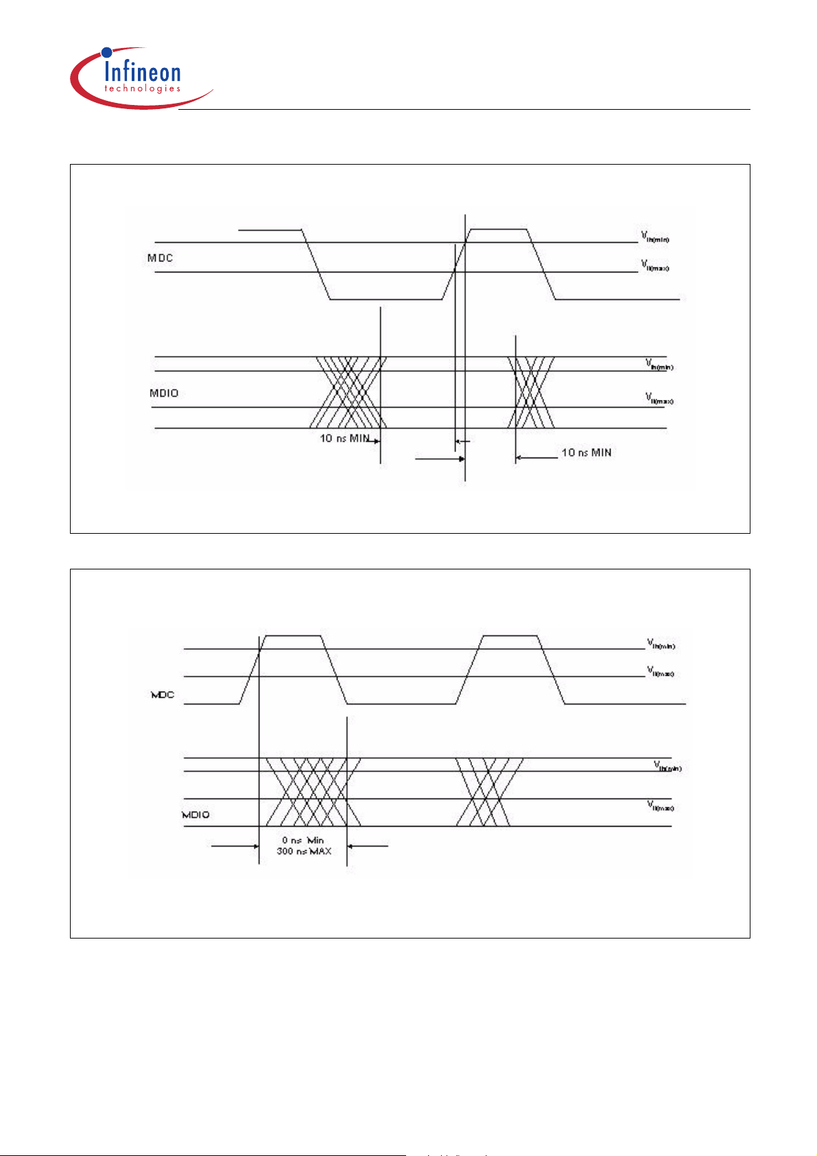
ADM8515/X
Electrical Characteristics
Figure 9 MDIO Sourced by STA
Figure 10 MDIO Sourced by PHY
Data Sheet 81 Rev. 1.21, 2005-11-08

ADM8515/X
7 Packaging
Package Outline of ADM8515/X
Packaging
Figure 11 P-LQFP-100-1 (Plastic Low Profile Quad Flat Package)
Note: Dimensions in mm
Data Sheet 82 Rev. 1.21, 2005-11-08

ADM8515/X
Packaging
Table 90 Dimensions for 100 Pin LQFP Package
Symbol Millimeter (mm) Inch
Min. Typ. Max. Min. Typ. Max.
A – –1.60– –0.063
A
1
A
2
0.05 – 0.15 0.002 – 0.006
1.35 1.40 1.45 0.053 0.005 0.057
D 16.00 BSC. 0.630 BSC.
D
1
14.00 BSC 0.551 BSC.
E 16.00 BSC 0.630 BSC.
E
1
R
2
R
1
0.08 – 0.20 0.003 – 0.008
0.08 – – 0.003 – –
14.00 BSC 0.551 BSC.
Θ 0° 3.5° 7° 0° 3.5° 7°
Θ
1
Θ
2
Θ
3
0° – – 0° – –
11° 12° 13° 11° 12° 13°
11° 12° 13° 11° 12° 13°
c 0.09 – 0.20 0.004 – 0.008
L 0.45 0.60 0.75 0.018 0.024 0.030
L
1
1.00 Ref. 0.039 Ref.
S 0.20 – – 0.008 – –
b 0.17 0.20 0.27 0.007 0.008 0.011
e 0.50 BSC. 0.020 BSC.
D
2
E
2
12.00 0.472
12.00 0.472
Tolerance of Form and Position
aaa 0.20 0.008
bbb 0.20 0.008
ccc 0.08 0.003
ddd 0.08 0.003
Data Sheet 83 Rev. 1.21, 2005-11-08

ADM8515/X
Appendix
8Appendix
8.1 Appendix 1 EEPROM CONTENT & Example
The EEPROM contents from offset 0 to offset5 is “FF_FF_FF_FF_FF_FF”, the EEPROM isn’t programmed
correctly. The default values for every field are used instead of loading from EEPROM.
Offset (byte) Field Description
00 node_id0 The 1st byte of Ethernet node ID.
01 node_id1 The 2nd byte of Ethernet node ID.
02 node_id2 The 3rd byte of Ethernet node ID.
03 node_id3 The 4th byte of Ethernet node ID.
04 node_id4 The 5th byte of Ethernet node ID.
05 node_id5 The 6th byte of Ethernet node ID.
06-07 signature 0x8515
08 max_pwr The maximum USB power consumption.
09 ep3_interval The polling interval for endpoint 3. If this value is 0, EP3 is
disabled.
0A[0] reserved
0A[1] usb_sel 0A[1] = 0: select external USB 2.0 transceiver
OA[1] = 1: select internal USB 2.0 transceiver.
0A[4:2] Phy MODE 0A[4:2] = 000: tri-state MII pins
0A[6] Bus power selection 0A[6] = 0: bus power
0A[6] = 1: self power
0A[7] Remote wake up 0A[7] = 0: with wakeup cap
0A[7] = 1: without wakeup cap
0B[5:0] reserved
0B[7:6] LED mode Refer to Pin description
0C Languageid_lo The low byte of language ID.
0D Languageid_hi The high byte of language ID.
0E-0F reserved
10 manuid_lo The low byte of manufacture ID.
11 manuid_hi The high byte of manufacture ID.
12 proid_lo The low byte of product ID.
13 proid_hi The high byte of product ID.
14 manu_str_len The length for manufacture string.
15 manu_str_offset The word offset address of manufacture string.
16 pro_str_len The length for product string.
17 pro_str_offset The word offset address of product string.
18 seri_str_len The length for serial number string.
19 seri_str_offset The word offset address of serial number string.
Data Sheet 84 Rev. 1.21, 2005-11-08

ADM8515/X
Table 91 Example
Offset (byte) Value
0000
0008
0010
0018
0020
0028
0030
0038
0040
0048
0050
0058
0060
0068
0070
0078
H
H
H
H
H
H
H
H
H
H
H
H
H
H
H
H
00 00 E8 00 02 2C 00 00
50 01 02 00 09 04 00 00
A6 07 15 85 0E 10 2A 20
0A 38 00 00 00 00 00 00
0E 03 41 00 44 00 4D 00
74 00 65 00 6B 00 00 00
1E 00 55 00 53 00 42 00
20 00 31 00 30 00 2F 00
2A 03 55 00 53 00 42 00
20 00 54 00 6F 00 20 00
4C 00 41 00 4E 00 20 00
43 00 6F 00 6E 00 76 00
65 00 72 00 74 00 65 00
72 00 00 00 00 00 00 00
0A 03 30 00 30 00 30 00
31 00 00 00 00 00 00 00
Appendix
Offset (byte) Value Description
00-05 00_00_E8_10_46_02 NIC node ID
08 50 Maximum power 160 mA
09 01 Interrupt endpoint 3 polling interval 1ms
0A 02 Isochronous endpoint disable, select internal USB
transceiver, use bus power. Use internal Ethernet PHY,
Wake on LAN enable
0C-0D 0904 Language ID 0409
10-11 A607 Manufacture ID 07A6
12-13 8515 Product ID 8515
14 0E Manufacture string length 0E bytes
15 10 Manufacture string starts from word offset 10
offset 20
.
H
, thus byte
H
16 1E Product string length 1E bytes
17 18 Product string starts from word offset 18
30
.
H
, thus byte offset
H
18 0A Serial number string length 0A bytes
19 38 Serial number string starts from word offset 38
20-2E 0E 03 41 00 44 00 4D 00
74 00 65 00 6B 00
offset 70
0E:descriptor size 14 bytes
03: string descriptor
.
H
, thus byte
H
41........: UNICODE encoded string
Data Sheet 85 Rev. 1.21, 2005-11-08

ADM8515/X
Offset (byte) Value Description
30-4E 1E 03 55 00 53 00 42
0020 00................
50-5A 0A 03 30 00 30 00 30
0031 00
1E:descriptor size 30 bytes
03: string descriptor
55........: UNICODE encoded string
0A: descriptor size 10 bytes
03: string descriptor
30........: UNICODE encoded string
Appendix
Data Sheet 86 Rev. 1.21, 2005-11-08

Terminology
A
ACK Acknowledge
B
BIST Built In Self Test
C
COL Collision
CRC Cyclic Redundancy Check
CRS Carrier Sense
D
DC Direct Current
DM Differential Minus
DP Differential Plus
E
EP End Point
ESD Electro Static Discharge
F
FIFO First In First Out
FLP First Link Pulse
G
GPIO General Purpose Input Output
H
HW Hardware
I
I/O Input/Output
IA Information Appliance
ISI Inter-symbol Interface
L
LAN Local Area Network
LED Light Emitting Diode
LH Latch High
LQFP Low Profile Quad Flat Package
LS Least Significant Bit
M
MAC Media Access Controller
MDC Management Data Clock
MDIO Management Data Input/Output
MFG Manufacture Program
MII Media Independent Interface
N
NAK Not Acknowledge
NLP Normal Link Pulse
ADM8515/X
Data Sheet 87 Rev. 1.21, 2005-11-08

O
OS Operating System
OUI Organizationally Unique Identifier
P
PPower Pin
PHY Physical Layer
PIE Parallel Interface Engine
PMD Physical Medium Dependent
R
RX Receive
RXCLK Receive Clock
RXD Receive Data
RXDV Receive Data Valid
S
SQE Signal Quality Error
SW Software
T
TX Transmit
TXCLK Transmit Clock
TXD Transmit Data
TXIN Transmit Input Negative
TXIP Transmit Input Positive
U
USB Universal Serial Bus
UTMI USB 2.0 Transceiver Macrocell Interface
V
VDD Voltage
VIN Voltage In
VOUT Voltage out
W
WAN Wide Area Network
X
XCVR Transceiver
xDSL A/S/V DSL
ADM8515/X
Data Sheet 88 Rev. 1.21, 2005-11-08

www.infineon.com
Published by Infineon Technologies AG
 Loading...