


LM-400
Page Number : 1 of 6
Bluetooth Module - Part Code LM-400
Top view Bottom view
Contents:
1. Device Overall Description
2. Bluetooth
-Features
-Speci cation Compliance
-Bluetooth Block Diagram
-Modulation Methods
- Power Consumption
- RF Characteristics
3. Pinout and nition
4. Mechanical Dimension
Side view

Device Overall Description
The BTM400 is designed to provide Bluetooth2.0 + EDR function on a small form factor. The Bluetooth function
is based on CSR BlueCore4-Ext Bluetooth System, which implements the full speed class 1 Bluetooth operations
with full 7 slave piconet support. The interface of BTM400 to host system is UART.
Bluetooth
Features
-CSR BlueCore4
-Bluetooth 2.0 + EDR support
-Full Speed Class 1 Bluetooth operation with full 7 slave piconet support
-Single onboard Antenna connector support (Optional)
-Chip antenna on board
Bluetooth Block Diagram
BC04
Chip Antenna
Or
RF I-PEX
Connector
Modulation Methods
FHSS ( Frequency Hopping Spread Spectrum ) defined in Bluetooth Specification.
Basic Data Rate
Enhanced Data Rate
Class1
Module
Data Rate Modulation scheme
1 Mbps GFSK
2Mbps π/4 – DQPSK
3Mbps 8DPSK
H/W Flow
Control
UART
VDD
Host
Pin
header
LM-400
Page Number : 2 of 6
0121 270 6232 | www.lm-technologies.com | sales@lm-technologies.com
LM-400
Page Number : 3 of 6
0121 270 6232 | www.lm-technologies.com | sales@lm-technologies.com
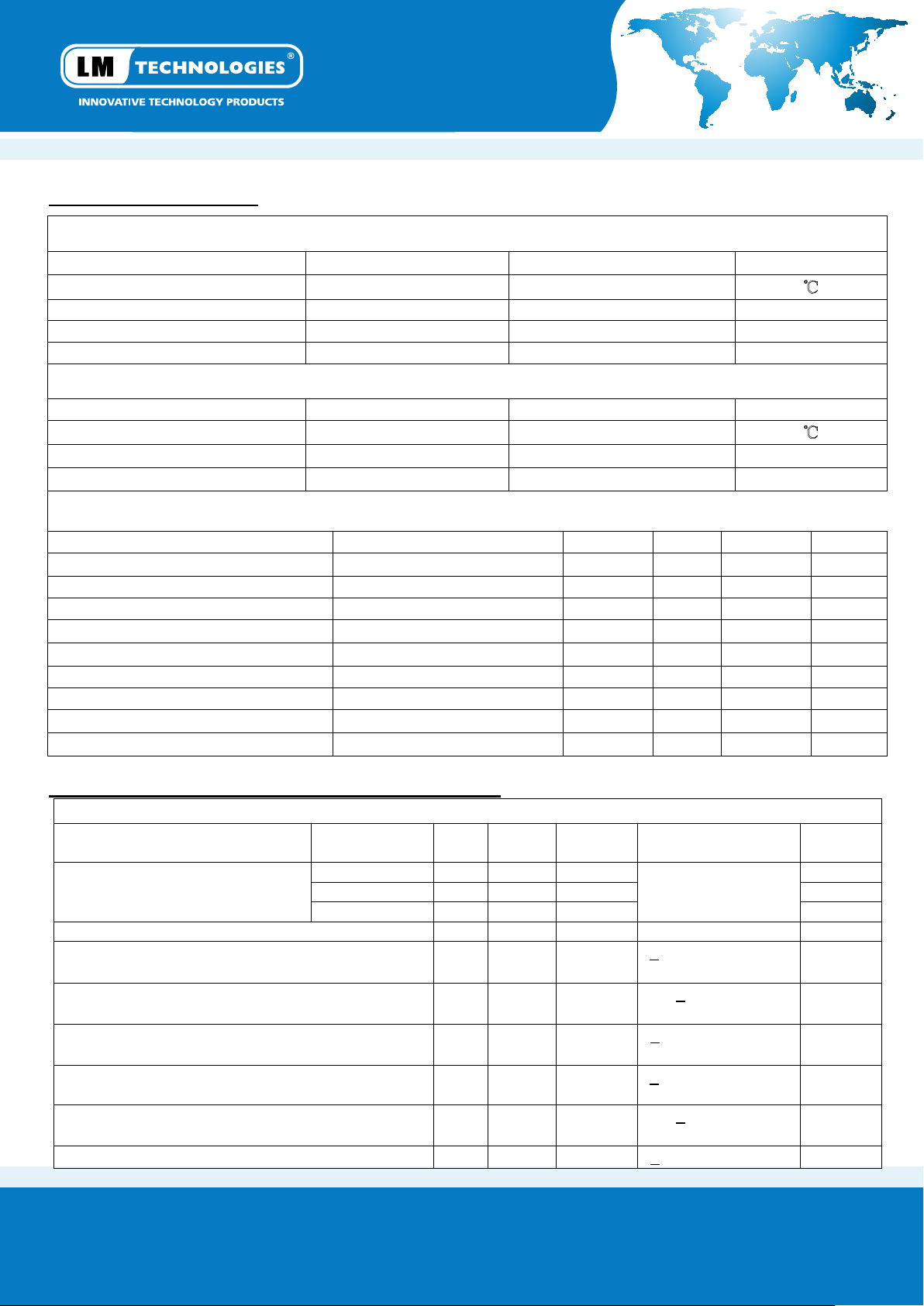
Bluetooth Power Consumption
Absolute Maximum Ratings
Parameter Min. Max. Unit
58+ 04- erutarepmeT egarotS
Other Pin Voltage Vss-0.4 VDD+0.4 DCV
Recommended Operating Conditions
Parameter Min. Max. Unit
07+ 01- erutarepmeT
General Electrical Specification
Parameter Description Min. Typ. Max. Unit
RF Output Power Measured in 50ohm 15 16.5 18 dBm
Load Impedance No abnormal Oscillation 5:1
Input Low Voltage RESET,UART,GPIO,PCM -0.30 - 0.80 DCV
Input High Voltage RESET,UART,GPIO,PCM 0.7VDD - VDD+0.3 DCV
Output Low Voltage UART,GPIO,PCM - - 0.40 DCV
Output High Voltage UART,GPIO,PCM VDD-0.4 - - DCV
Average Current Consumption Receive DM1 114 mA
℃
VCD 6.3 7.2 )DDV(egatloV ylppuS
VCD 3.3 0.3 )CCVP(egatloV ylppuS
℃
VCD 6.3 0.3 TRAU rof egatloV ylppuS
VCD 6.3 0.3 BSU rof egatloV ylppuS
zHG 084.2 204.2 ycneuqerF reirraC
mBd 68- 88- - ytivitisnes XR
Radio Characteristics - Basic Data Rate
Transmitter , VDD = 3.3V Temperature =+20°C
ycneuqerF
Min. Typ. Max. Bluetooth
(GHz)
Maximum RF transmit power
π/4 DQPSK
Maximum carrier frequency stability w
π/4 DQPSK
Maximum carrier frequency stability w
π/4 DQPSK
Maximum carrier frequency stability | w
8 DPSK
Maximum carrier frequency stability w
8 DPSK
Maximum carrier frequency stability w
(note)
2.480 - 7 -
- 2 -
0
- 6 -
i
- 8 -
+ wi |
0
- 2 -
0
- 6 -
i
Unit
Specification
mBd - 6 - 204.2
-6 to +20
<
±10 for all blocks
<
±75 for all
packets
<
±75 for all blocks
<
±10 for all blocks
<
±75 for all
packets
- 8 - KSPD 8
<
±75 for all blocks
mBd - 6 - 144.2
dBm
Bd 1+ ot 4- - 6.1- - rewop timsnart evitaleR
kHz
kHz
kHz
kHz
kHz
kHz

Maximum carrier frequency stability | w0 + wi |
π/4 DQPSK
Modulation Accuracy
8 DPSK
Modulation Accuracy
RMS DVEM -
99% DEVM Peak DEVM RMS DVEM -
99% DEVM Peak DEVM -
F>F0+3 MHz
- <-50 -
7
13
19
7
13
17
F<F0-3 MHz - <-50 F=F0-3 MHz - -46 -
In-band spurious emissions
F=F0-2 MHz - -34 F=F0-1 MHz - -35 F=F0+1 MHz - -35 F=F0+2 MHz - -31 F=F
+3 MHz - -33 -
0
EDR Differential Phase Encoding No
Errors
Receiver , VDD = 3.3V Temperature =+20°C
Sensitivity at 0.1% BER
Maximum received signal level
at 0.1% BER
C/I co-channel at 0.1% BER
Adjacent channel selectivity C/I
+1 MHz
F=F
0
Adjacent channel selectivity C/I
-1 MHz
F=F
0
Adjacent channel selectivity C/I
+2 MHz
F=F
0
Adjacent channel selectivity C/I
-2 MHz
F=F
0
Adjacent channel selectivity C/I
+3 MHz
F=F
0
Adjacent channel selectivity C/I
F=F
-5 MHz
0
F0= 2405, 2441, 2477 MHz
Adjacent channel selectivity C/I
F=F
image
π/4 DQPSK
8 DPSK - -78 π/4 DQPSK
8 DPSK - -10 π/4 DQPSK
8 DPSK - 19 π/4 DQPSK
8 DPSK - -5 π/4 DQPSK
8 DPSK - -5 π/4 DQPSK
8 DPSK - -40 π/4 DQPSK
8 DPSK - -20 π/4 DQPSK
8 DPSK - -45 π/4 DQPSK
8 DPSK - -45 -
π/4 DQPSK
8 DPSK -15
- -87 -
- -8 -
- 10 -
- -10 -
- -11 -
- -40 -
- -23 -
- -45 -
- -45 -
-20
- < 20 %
- < 30 %
- <
35 %
- < 13 %
- < 20 %
- <
25 %
< -40
<
-40
<
-40
<
-20
<
-26
<
-26
<
-20
<
-40
dBm
dBm
dBm
dBm
dBm
dBm
dBm
dBm
> 99 %
htooteulB .xaM .pyT.niM noitaludoM
Unit
Specification
< -70
-70
<
> -20
>
-20
< +13
+21
<
< 0
+5
<
< 0
<
+5
< -30
-25
<
< -20
-13
<
< -40
<
-33
< -40
<
-33
< -7
<
0
dBm
dBm
dBm
dBm
dB
dB
dB
dB
dB
dB
dB
dB
dB
dB
dB
dB
dB
dB
dB
dB
Note :
Measurement made using a PO WER_TABLE entery of TX_PRE 80, INT PA63, EXT PA255. This ensures that the
Bluetooth requirements for ACP and those defined by the FCC and ETSI are satisfied over the operating
temp erature rang of -5Ð to + 45Ð . Although the design is capable of generating in excess of + 18dBm,
regulatory compliance over the full temperature range of -5Ð to + 45Ð will not be satisfied if the transmit power
approaches this value.
LM-400
Page Number : 4 of 6
0121 270 6232 | www.lm-technologies.com | sales@lm-technologies.com

Part Number LM-400
Page Number : 5 of 6
0121 270 6232 | www.lm-technologies.com | sales@lm-technologies.com
Radio Characteristics – Enhanced Data Rate
Transmitter , VDD = 3.3V Temperature =+20°C
ycneuqerF
Min. Typ. Max. Bluetooth
(GHz)
Maximum RF transmit power
π/4 DQPSK
Maximum carrier frequency stability w
π/4 DQPSK
Maximum carrier frequency stability w
π/4 DQPSK
Maximum carrier frequency stability | w
8 DPSK
Maximum carrier frequency stability w
8 DPSK
Maximum carrier frequency stability w
8 DPSK
Maximum carrier frequency stability | w
π/4 DQPSK
Modulation Accuracy
8 DPSK
Modulation Accuracy
In-band spurious emissions
EDR Differential Phase Encoding No
Receiver , VDD = 3.3V Temperature =+20°C
Sensitivity at 0.1% BER
Maximum received signal level
at 0.1% BER
C/I co-channel at 0.1% BER
Adjacent channel selectivity C/I
+1 MHz
F=F
0
(note)
2.480 - 7 -
- 2 -
0
- 6 -
i
- 8 -
+ wi |
0
- 2 -
0
- 6 -
i
- 8 -
+ wi |
0
RMS DVEM -
99% DEVM Peak DEVM RMS DVEM -
99% DEVM Peak DEVM -
F>F0+3 MHz
- <-50 -
7
13
19
7
13
17
F<F0-3 MHz - <-50 F=F0-3 MHz - -46 F=F0-2 MHz - -34 F=F0-1 MHz - -35 F=F0+1 MHz - -35 F=F0+2 MHz - -31 -
+3 MHz - -33 -
F=F
0
Errors
π/4 DQPSK
- -87 -
8 DPSK - -78 π/4 DQPSK
- -8 -
8 DPSK - -10 π/4 DQPSK
- 10 -
8 DPSK - 19 π/4 DQPSK
- -10 -
8 DPSK - -5 -
Unit
Specification
-6 to +20
dBm
<
±10 for all blocks
<
±75 for all
kHz
kHz
packets
<
±75 for all blocks
<
±10 for all blocks
<
±75 for all
kHz
kHz
kHz
packets
<
±75 for all blocks
kHz
- < 20 %
- < 30 %
- <
35 %
- < 13 %
- < 20 %
- <
25 %
< -40
<
-40
<
-40
<
-20
<
-26
<
-26
<
-20
<
-40
dBm
dBm
dBm
dBm
dBm
dBm
dBm
dBm
> 99 %
htooteulB .xaM .pyT.niM noitaludoM
Unit
Specification
< -70
<
-70
> -20
-20
>
< +13
+21
<
< 0
<
+5
dBm
dBm
dBm
dBm
dB
dB
dB
dB
mBd - 6 - 204.2
mBd - 6 - 144.2
Bd 1+ ot 4- - 6.1- - rewop timsnart evitaleR

Part Number LM-400
Page Number : 5 of 6
0121 270 6232 | www.lm-technologies.com | sales@lm-technologies.com
Adjacent channel selectivity C/I
-1 MHz
F=F
0
Adjacent channel selectivity C/I
+2 MHz
F=F
0
Adjacent channel selectivity C/I
-2 MHz
F=F
0
Adjacent channel selectivity C/I
+3 MHz
F=F
0
Adjacent channel selectivity C/I
-5 MHz
F=F
0
F0= 2405, 2441, 2477 MHz
Adjacent channel selectivity C/I
F=F
image
Pinout and Definition
π/4 DQPSK
- -11 -
8 DPSK - -5 π/4 DQPSK
- -40 -
8 DPSK - -40 π/4 DQPSK
- -23 -
8 DPSK - -20 π/4 DQPSK
- -45 -
8 DPSK - -45 π/4 DQPSK
- -45 -
8 DPSK - -45 -
π/4 DQPSK
-20
8 DPSK -15
< 0
+5
<
< -30
-25
<
< -20
<
-13
< -40
-33
<
< -40
-33
<
< -7
<
0
dB
dB
dB
dB
dB
dB
dB
dB
dB
dB
dB
dB

Part Number LM-400
Page Number : 6 of 6
0121 270 6232 | www.lm-technologies.com | sales@lm-technologies.com
Mechanical Dimension
-30mm x 27.5mm (L x W) +- 0.15mm
-Component height (unit: mm)
Notes
:
1. PIN9,10 DSR/DTR don’t use, they are no function currently.
2. PIN5 Pairing, the function have been changed to Data led indication
3. PIN6 Status, the function have not been specified.
4. RESET KEY
By pressing the Reset button, you can:
Disconnect and reconnect a wireless connection (a short press).
Restore the factory COM port 19200bps settings (over three seconds' press).
5. LED
Bluetooth link status

Part Number LM-400
Page Number : 5 of 6
Pin N o.
Pin N a me
Pin Type
Descr iption
1
G ND
G ND
C ommon ground
2
P VC C
Power
Power Amp. Power Supply(3.3V)
3
AIO (0)
Bi -directional
Programmable I/O terminal , 32KHz sleep clock input
4
AIO (1)
Bi -directional
Programmable I/O terminal
5
P IO (0)
Bi -directional
Programmable I/O terminal , RX Enable
6
PIO (1)
Bi -directional
Programmable I/O terminal , TX Enable
7
PIO (2)
Bi -directional
Programmable I/O terminal , USB_PULL_UP , C LK_REQ _O UT
8
PIO (3)
Bi -directional
Programmable I/O terminal , USB_WAK E_UP , CLK_REQ _IN
9
PIO (4)
Bi -directional
Programmable I/O terminal , USB_O N , BT_Priority/C h_Clk output for
co-existence signalling
10
G ND
G ND
C ommon ground
11
PIO (5)
Bi -directional
Programmable I/O terminal , USB_DETAC H , BT_Active output for co -
existence signalling
12
PIO (6)
Bi -directional
Programmable I/O terminal , CLK_REQ , WLAN_Active/C h_Data input
for for co-existence signalling
13
PIO (7)
Bi -directional
Programmable I/O terminal
14
PIO (8)
Bi -directional
Programmable I/O terminal
15
PIO (9)
Bi -directi onal
Programmable I/O terminal
16
RESET
C MO S input
Reset input of module, Active low reset
17
VC C
Power
Module power supply input
18
G ND
G ND
C ommon ground
19
G ND
G ND
C ommon ground
20
USB_DP
Bi -directional
USB data plus
21
USB_DN
Bi -directional
USB da ta minus
22
PCM_SYNC
Bi -directional
Synchronous data sync
23
PCM_IN
C MO S input
Synchronous data input
24
PCM_O UT
C MO S output
Synchronous data output
25
PCM_C LK
Bi -directional
Synchronous data clock
26
UART_RX
C MO S input
UART data input
27
UART_TX
C MO S output
UART data output
28
UART_RTS
C MO S output
UART request to send(active low)
29
G ND
G ND
C ommon ground
30
UART_C TS
C MO S input
UART clear to send(active low)
31
SPI_MO SI
C MO S input
Serial Peripheral Interface data input
32
SPI_CSB
C MO S input
C hip select for Synchronous Serial Interface(active low)
33
SPI_CLK
C MO S input
Serial Peripheral Interface clock
34
SPI_MISO
C MO S output
Serial Peripheral Interface data output
35
PIO (11)
Bi -directional
Programmable I/O terminal
36
PIO (10)
Bi -directional
Programmable I/O terminal
37
RF_IO
Analogue
Antenna interface
38
G ND
G ND
C ommon ground
0121 270 6232 | www.lm-technologies.com | sales@lm-technologies.com

This device complies with the following radio frequency and safety standards.
Important to OEM Manufacturer:
This following FCC Warning must be included in the HOST User Manual.
FCC Warning
This device complies with Part 15 of the FCC Rules. Operation is
subject to the following two conditions:
(1) this device may not cause harmful interference, and (2) this device must accept any
interference received, including interference that may cause undesired operation.
NOTE 1: Any changes or modifications to this unit not expressly approved by the party
responsible for compliance could void the user's authority to operate the equipment.
FCC Radiation Exposure Statement:
This equipment complies with FCC radiation exposure limits set forth for an uncontrolled
environment. End users must follow the specific operating instructions for satisfying RF exposure
compliance.
Note 1: This module certified that complies with RF exposure requirment under mobile or fixed
condition, this module is to be installed only in portable or mobile or fixed appl ica tions.
A mobile device is defined as a transmitting device designed to be used in other than fixed
locations and to generally be used in such a way that a separation distance of at least 20
centimeters is normally maintained between the transmitter's radiating structure(s) and the body of
the user or nearby persons. Transmitting devices designed to be used by consumers or workers
that can be easily re-located, such as wireless devices associated with a personal computer, are
considered to be mobile devices if they meet the 20 centimeter separation requirement.
A fixed device is defined as a device is physically secured at one location and is not able to be
easily moved to another location.
Note 2: Any modifications made to the module will void the Grant of Certification, this module is
limited to OEM installation only and must not be sold to end-users, end-user has no manual
instructions to remove or install the device, only software or operating procedure shall be placed
in the end-user operating manual of final products.
Note 3: The device must not transmit simultaneously with any other antenna or transmitter.
Note 4: To ensure compliance with all non-transmitter functions the host manufacturer is
responsible for ensuring compliance with the module(s) installed and fully operational. For

example, if a host was previously authorized as an unintentional radiator under the Declaration of
Conformity procedure without a transmitter certified module and a module is added, the host
manufacturer is responsible for ensuring that the after the module is installed and operational the
host continues to be compliant with the Part 15B unintentional radiator requirements. Since this
may depend on the details of how the module is integrated with the host, LM Technologies Ltd.
shall provide guidance to the host manufacturer for compliance with the Part 15B requirements.
Note 5: FCC ID label on the final system must be labeled with “Contains FCC ID:
VVXLM400-1” or “Contains transmitter module FCC ID: VVXLM400-1”.
The transmitter module must be installed and used in strict accordance with the manufacturer's
instructions as described in the user documentation that comes with the host product. LM
Technologies Ltd. is responsible for the compliance of the module in all final hosts.
 Loading...