

- 1-1 -
[CONTENTS]
❍ SECTION 1.GENERAL
• SERVICING PRECAUTIONS . . . . . . . . . . . . . . . . . . . . . . . . . . . . . . . . . . . . . . . . . . . . . . . 1-2
• ESD PRECAUTIONS . . . . . . . . . . . . . . . . . . . . . . . . . . . . . . . . . . . . . . . . . . . . . . . . . . . . . 1-4
❍ SECTION 2.ELECTRICAL SECTION
• TROUBLESHOOTING GUIDE . . . . . . . . . . . . . . . . . . . . . . . . . . . . . . . . . . . . . . . . . . . . . . 2-1
• INTERNAL BLOCK DIAGRAM of ICs . . . . . . . . . . . . . . . . . . . . . . . . . . . . . . . . . . . . . . . . . 2-21
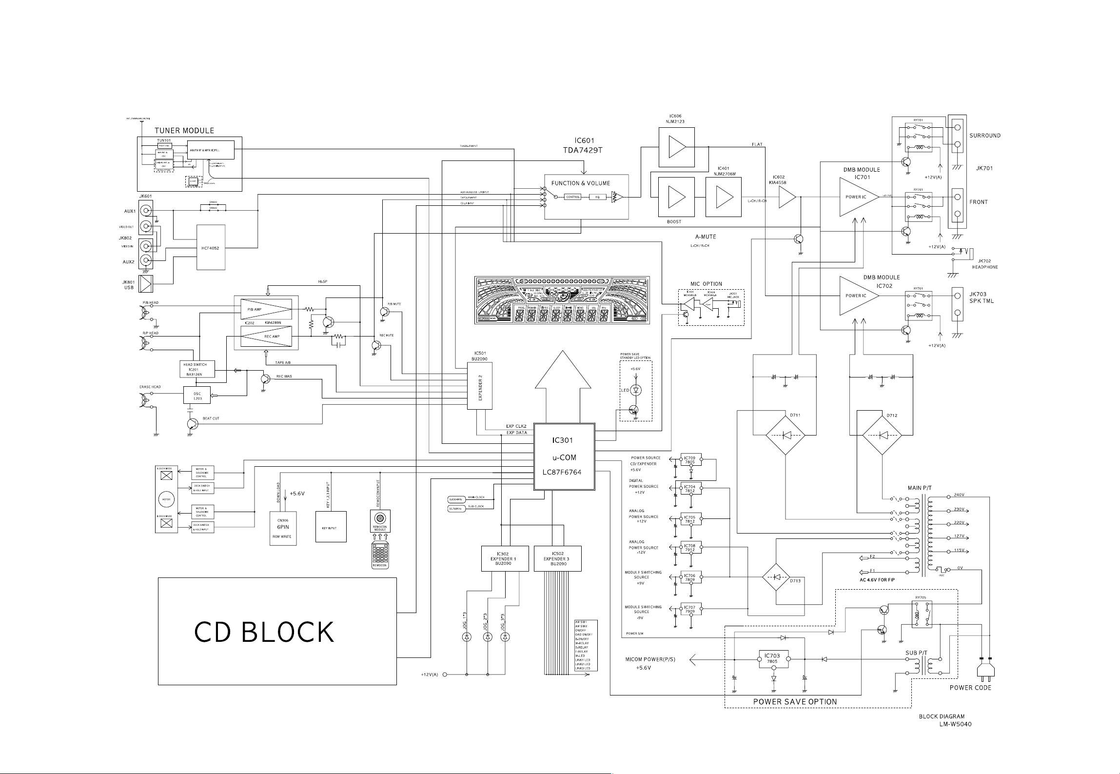
• BLOCK DIAGRAM . . . . . . . . . . . . . . . . . . . . . . . . . . . . . . . . . . . . . . . . . . . . . . . . . . . . . . . 2-25
• SCHEMATIC DIAGRAMS . . . . . . . . . . . . . . . . . . . . . . . . . . . . . . . . . . . . . . . . . . . . . . . . . 2-27
• WIRING DIAGRAM . . . . . . . . . . . . . . . . . . . . . . . . . . . . . . . . . . . . . . . . . . . . . . . . . . . . . . 2-39
• PRINTED CIRCUIT BOARD DIAGRAM . . . . . . . . . . . . . . . . . . . . . . . . . . . . . . . . . . . . . . . 2-41
❍ SECTION 3. EXPLODED VIEWS . . . . . . . . . . . . . . . . . . . . . . . . . . . . . . . . . . . 3-1
❍ SECTION 4. SPEAKER PART . . . . . . . . . . . . . . . . . . . . . . . . . . . . . . . . . . . . . 4-1
❍ SECTION 5. REPLACEMENT PARTS . . . . . . . . . . . . . . . . . . . . . . . . . . . . . . . 5-1
- 1-2 -
SECTION 1. GENERAL
❏ SERVICING PRECAUTIONS
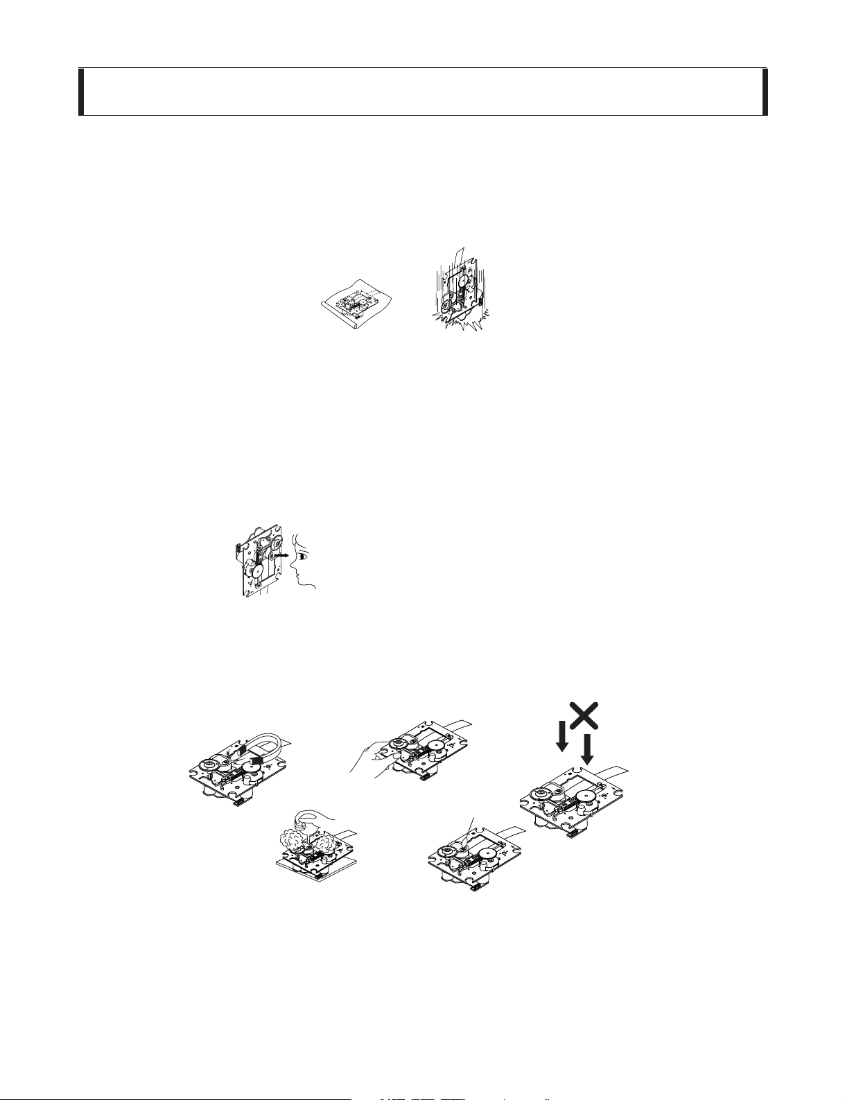
NOTES REGARDING HANDLING OF THE PICK-UP
1. Notes for transport and storage
1) The pick-up should always be left in its conductive bag until immediately prior to use.
2) The pick-up should never be subjected to external pressure or impact.
2. Repair notes
1) The pick-up incorporates a strong magnet, and so should never be brought close to magnetic materials.
2) The pick-up should always be handled correctly and carefully, taking care to avoid external pressure and
impact. If it is subjected to strong pressure or impact, the result may be an operational malfunction and/or
damage to the printed-circuit board.
3) Each and every pick-up is already individually adjusted to a high degree of precision, and for that reason
the adjustment point and installation screws should absolutely never be touched.
4) Laser beams may damage the eyes!
Absolutely never permit laser beams to enter the eyes!
Also NEVER switch ON the power to the laser output part (lens, etc.) of the pick-up if it is damaged.
5) Cleaning the lens surface
If there is dust on the lens surface, the dust should be cleaned away by using an air bush (such as used
for camera lens). The lens is held by a delicate spring. When cleaning the lens surface, therefore, a cotton
swab should be used, taking care not to distort this.
6) Never attempt to disassemble the pick-up.
Spring by excess pressure. If the lens is extremely dirty, apply isopropyl alcohol to the cotton swab. (Do
not use any other liquid cleaners, because they will damage the lens.) Take care not to use too much of
this alcohol on the swab, and do not allow the alcohol to get inside the pick-up.
Storage in conductive bag
Drop impact
NEVER look directly at the laser beam, and don’t let
contact fingers or other exposed skin.
Magnet
How to hold the pick-up
Conductive Sheet
Cotton swab
Pressure
Pressure
- 1-3 -
NOTES REGARDING COMPACT DISC PLAYER REPAIRS
1. Preparations
1) Compact disc players incorporate a great many ICs as well as the pick-up (laser diode). These components
are sensitive to, and easily affected by, static electricity. If such static electricity is high voltage, components
can be damaged, and for that reason components should be handled with care.
2) The pick-up is composed of many optical components and other high-precision components. Care must be
taken, therefore, to avoid repair or storage where the temperature of humidity is high, where strong magnetism is present, or where there is excessive dust.
2. Notes for repair
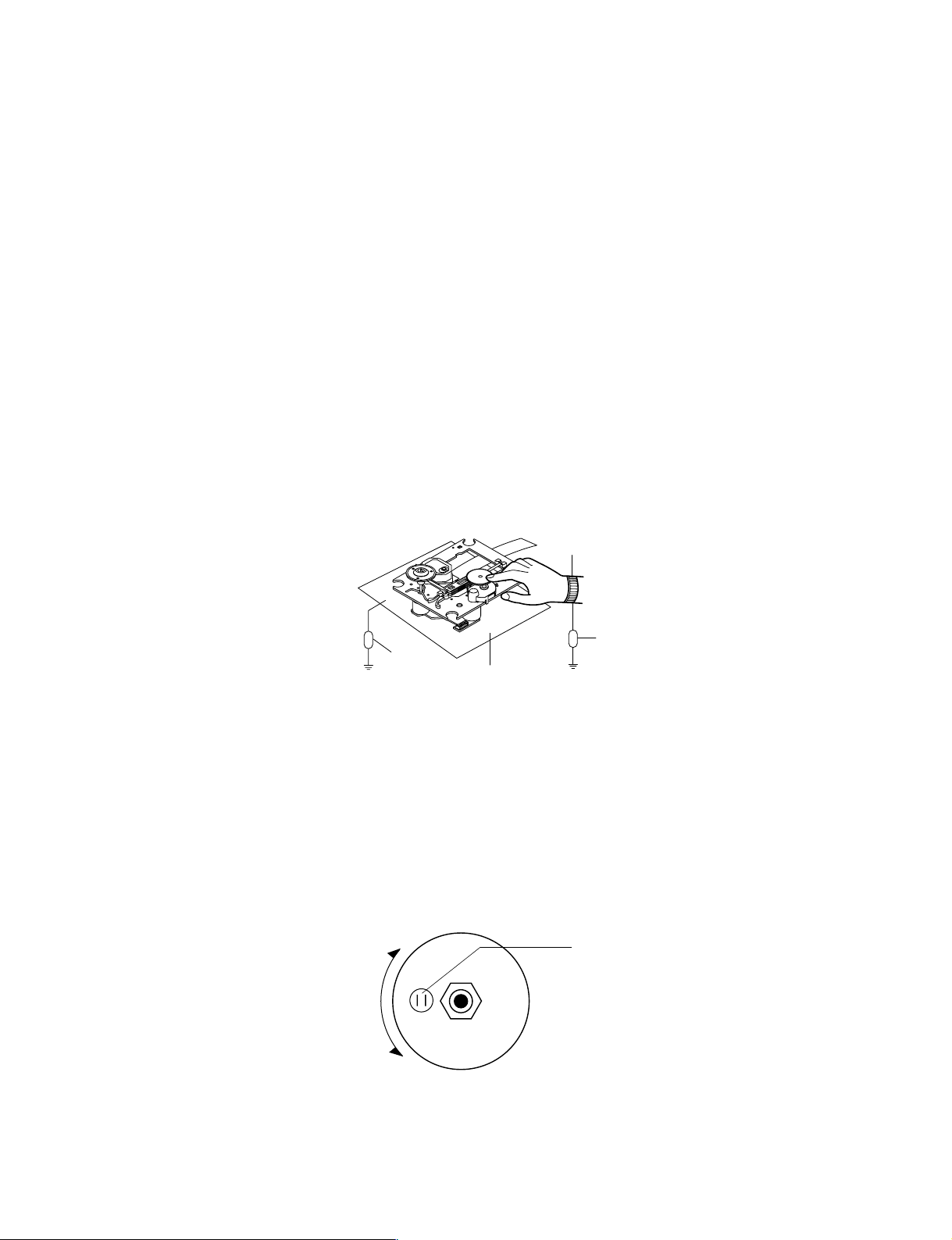
1) Before replacing a component part, first disconnect the power supply lead wire from the unit
2) All equipment, measuring instruments and tools must be grounded.
3) The workbench should be covered with a conductive sheet and grounded.
When removing the laser pick-up from its conductive bag, do not place the pick-up on the bag. (This is
because there is the possibility of damage by static electricity.)
4) To prevent AC leakage, the metal part of the soldering iron should be grounded.
5) Workers should be grounded by an armband (1M Ω)
6) Care should be taken not to permit the laser pick-up to come in contact with clothing, in order to prevent static electricity changes in the clothing to escape from the armband.
7) The laser beam from the pick-up should NEVER be directly facing the eyes or bare skin.
CLEARING MALFUNCTION
You can reset your unit to initial status if malfunction occur(button malfunction, display, etc.).
Using a pointed good conductor(such as driver), simply short the RESET jump wire on the inside of
the volume knob for more than 3 seconds.
If you reset your unit, you must reenter all its settings(stations, clock, timer)
NOTE: 1.To operate the RESET jump wire, pull the volume rotary knob and release it.
2. If you wish to operate the RESET jump wire, it is necessary to unplug the power cord.
Resistor
(1 Mohm)
Conductive
Sheet
Resistor
(1 Mohm)
Armband
RESET jump wire
VOLUME
VOLUME KNOB
DOWN
UP
- 1-4 -
❏ ESD PRECAUTIONS
Electrostatically Sensitive Devices (ESD)
Some semiconductor (solid state) devices can be damaged easily by static electricity. Such components
commonly are called Electrostatically Sensitive Devices (ESD). Examples of typical ESD devices are integrated
circuits and some field-effect transistors and semiconductor chip components.The following techniques should
be used to help reduce the incidence of component damage caused by static electricity.
1. Immediately before handling any semiconductor component or semiconductor-equipped assembly, drain off
any electrostatic charge on your body by touching a known earth ground. Alternatively, obtain and wear a
commercially available discharging wrist strap device, which should be removed for potential shock reasons
prior to applying power to the unit under test.
2. After removing an electrical assembly equipped with ESD devices, place the assembly on a conductive sur-
face such as aluminum foil, to prevent electrostatic charge buildup or exposure of the assembly.
3. Use only a grounded-tip soldering iron to solder or unsolder ESD devices.
4. Use only an anti-static solder removal device. Some solder removal devices not classified as "anti-static" can
generate electrical charges sufficient to damage ESD devices.
5. Do not use freon-propelled chemicals. These can generate electrical charges sufficient to damage ESD
devices.
6. Do not remove a replacement ESD device from its protective package until immediately before you are
ready to install it. (Most replacement ESD devices are packaged with leads electrically shorted together by
conductive foam, aluminum foil or comparable conductive materials).
7. Immediately before removing the protective material from the leads of a replacement ESD device, touch the
protective material to the chassis or circuit assembly into which the device will by installed.
CAUTION : BE SURE NO POWER IS APPLIED TO THE CHASSIS OR CIRCUIT, AND OBSERVE ALL
OTHER SAFETY PRECAUTIONS.
8. Minimize bodily motions when handing unpackaged replacement ESD devices. (Otherwise harmless motion
such as the brushing together of your clothes fabric or the lifting of your foot from a carpeted floor can generate static electricity sufficient to damage an ESD device).
CAUTION. GRAPHIC SYMBOLS
THE LIGHTNING FLASH WITH APROWHEAD SYMBOL. WITHIN AN EQUILATERAL TRIANGLE, IS
INTENDED TO ALERT THE SERVICE PERSONNEL TO THE PRESENCE OF UNINSULATED “DANGEROUS VOLTAGE” THAT MAY BE OF SUFFICIENT MAGNITUDE TO CONSTITUTE A RISK OF
ELECTRIC SHOCK.
THE EXCLAMATION POINT WITHIN AN EQUILATERAL TRIANGLE IS INTENDED TO ALERT THE
SERVICE PERSONNEL TO THE PRESENCE OF IMPORTANT SAFETY INFORMATION IN SERVICE
LITERATURE.
- 2-1 -
SECTION 2. ELECTRICAL
■ CD PART
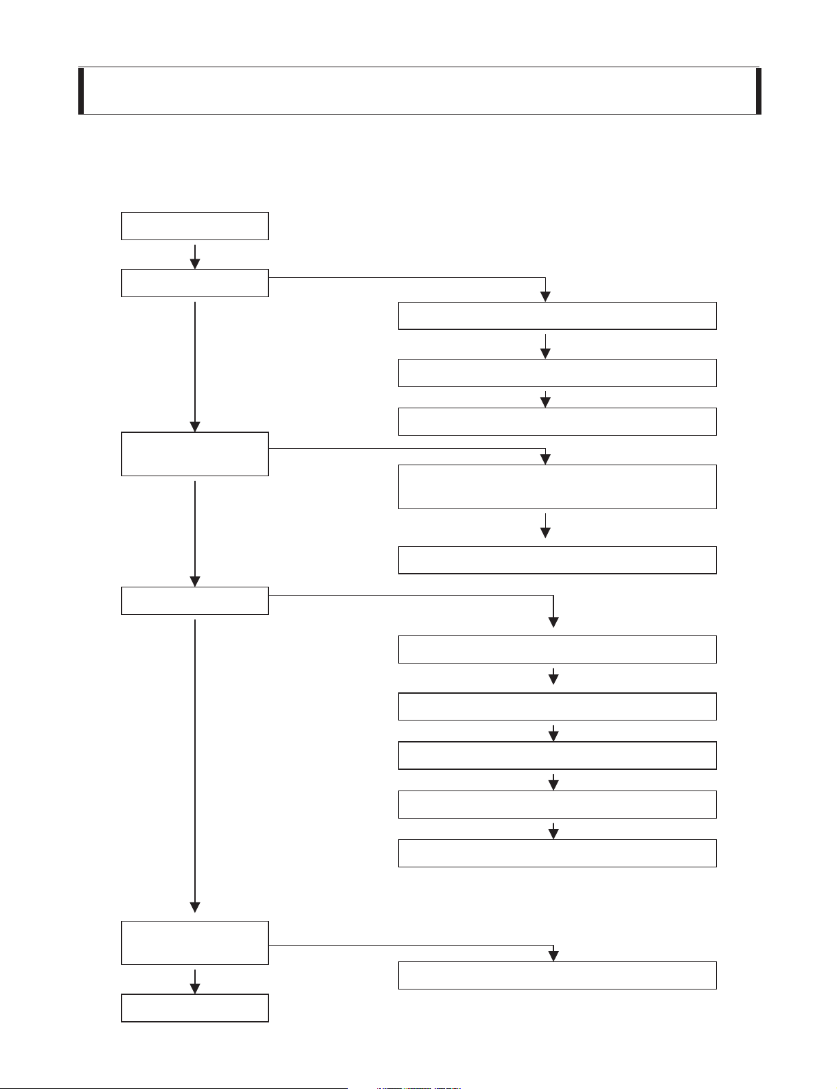
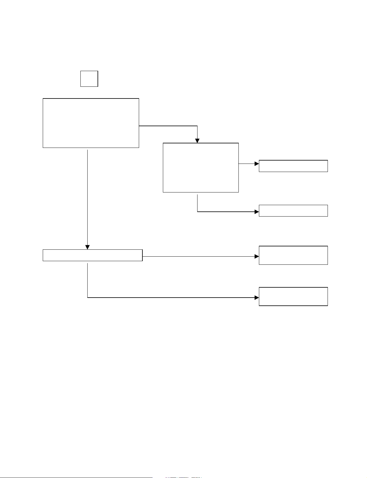
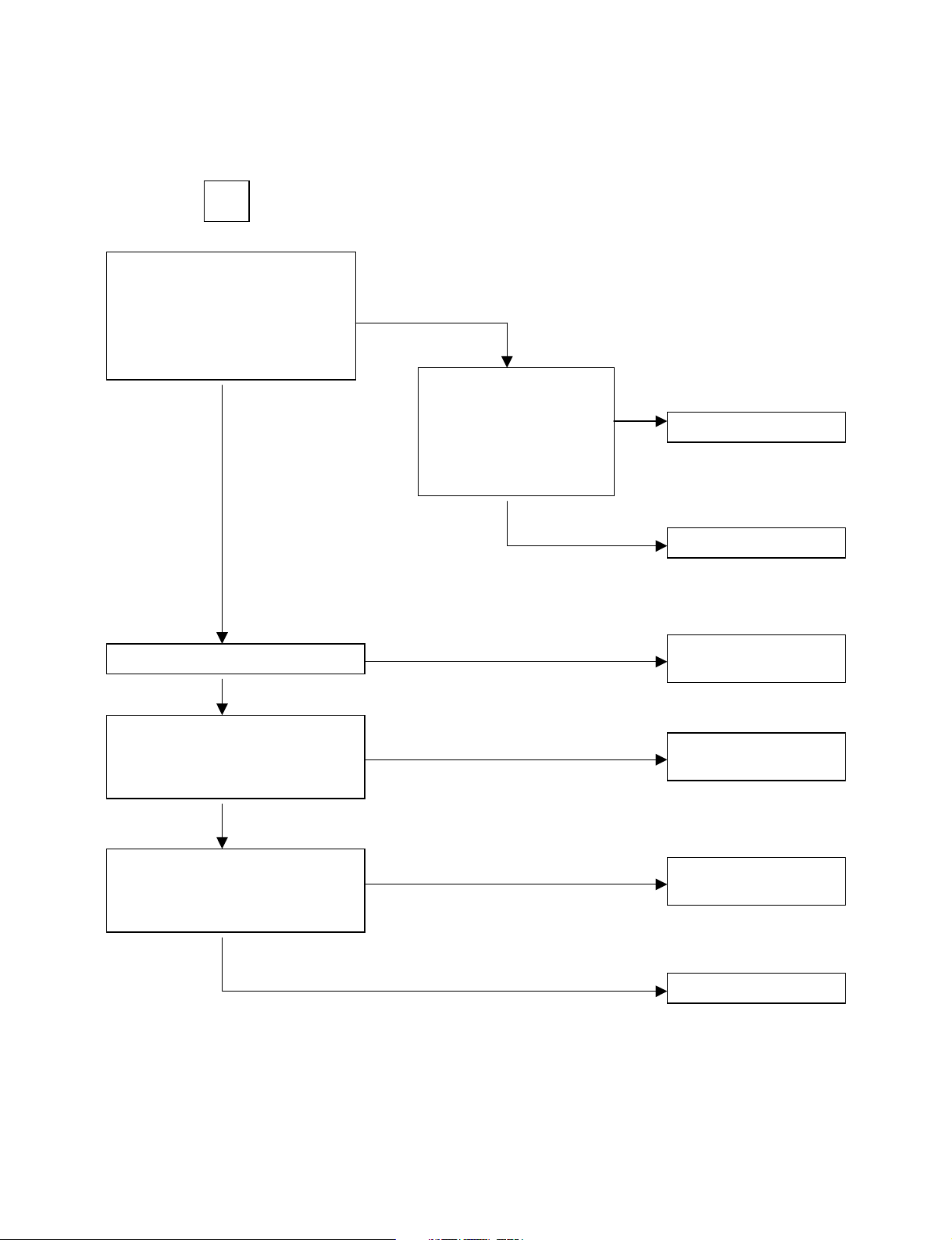
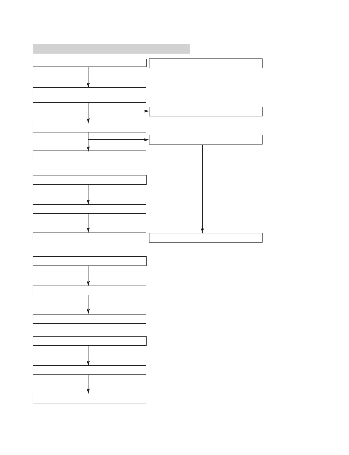
❏ TROUBLESHOOTING GUIDE
TURN ON CD
CONNECTOR CHECK ( PN808,PN807 )
CHECK POWER SUPPLY CIRCUIT( PN808 )
CHECK MICOM INTERFACE CIRCUIT( PN807 )
CHECK MICOM INTERFACE CIRCUIT( PN807 )
CONNECTOR CHECK(PN801,PN802)
CHECK PICKUP MOVEMENT
CHECK BA5810FP (IC803)
CHECK MN6627933CG (IC801)
CHECK AN22004 (IC802)
CONNECTOR CHECK (PN808)
CONNECTOR CHECK
( PN808,PN807,PN802,PN801 )
OPEN CLOSE CHECK
“ READING ”
DISPLAY CHECK
READING OK CHECK
IF PLAY, AUDIO
OUTPUT CHECK
OK
NO
NO
NO
NO
YES
YES
YES
YES
YES
- 2-2 -
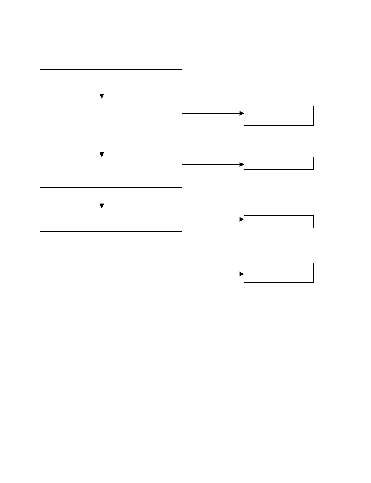
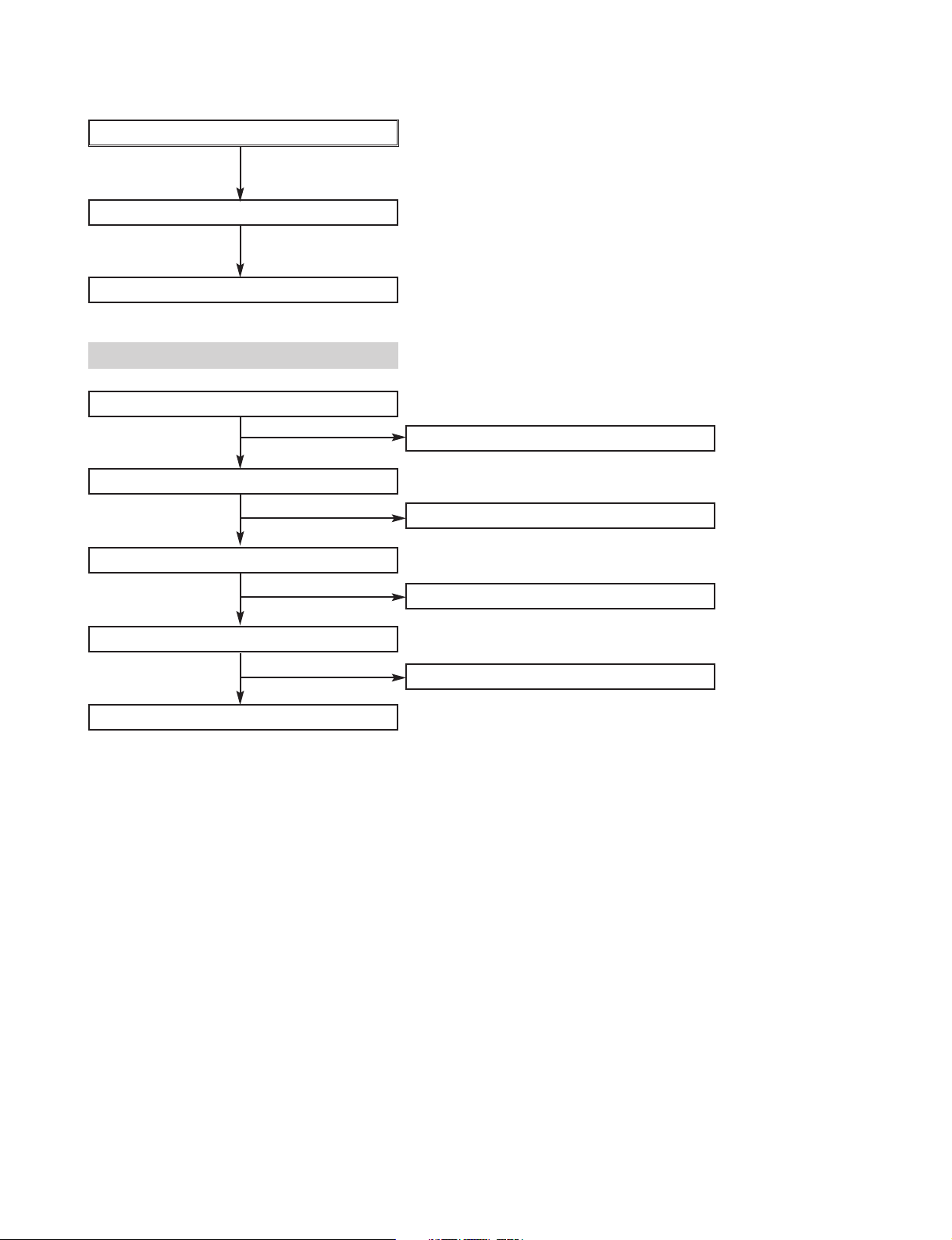
CONNECTOR LOCKING CHECK ( PN808,PN807 )
DEFECTIVE MAIN
POEWR SUPPLY
DEFECTIVE MICOM
DEFECTIVE IC803
DEFECTIVE
MECHANISM
CHECK POWER SUPPLY CIRCUIT( PN808 ,PN807)
PN808 PIN 5 = 6.2V, PIN 7 = 5V
PN807 PIN 1 = 5V
CHECK VOLTAGE CHANGE OF OPEN CLOSE ,
AND BTLMUTE VOLTAGE(= 5V)
(PN807 PIN 20:OPEN, 19:CLOSE, 4:BTLMUTE)
CHECK VOLTAGE CHANGE LO+, LO- OF IC803
(PN807, PIN OPEN:20, CLOSE:19)
YES
YES
YES
NO
NO
NO
NO
• OPEN CLOSE NG
- 2-3 -
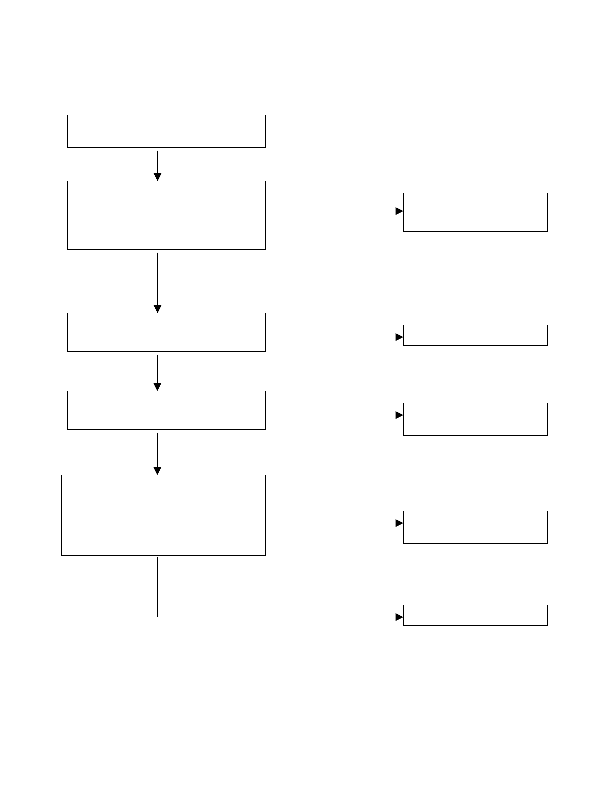
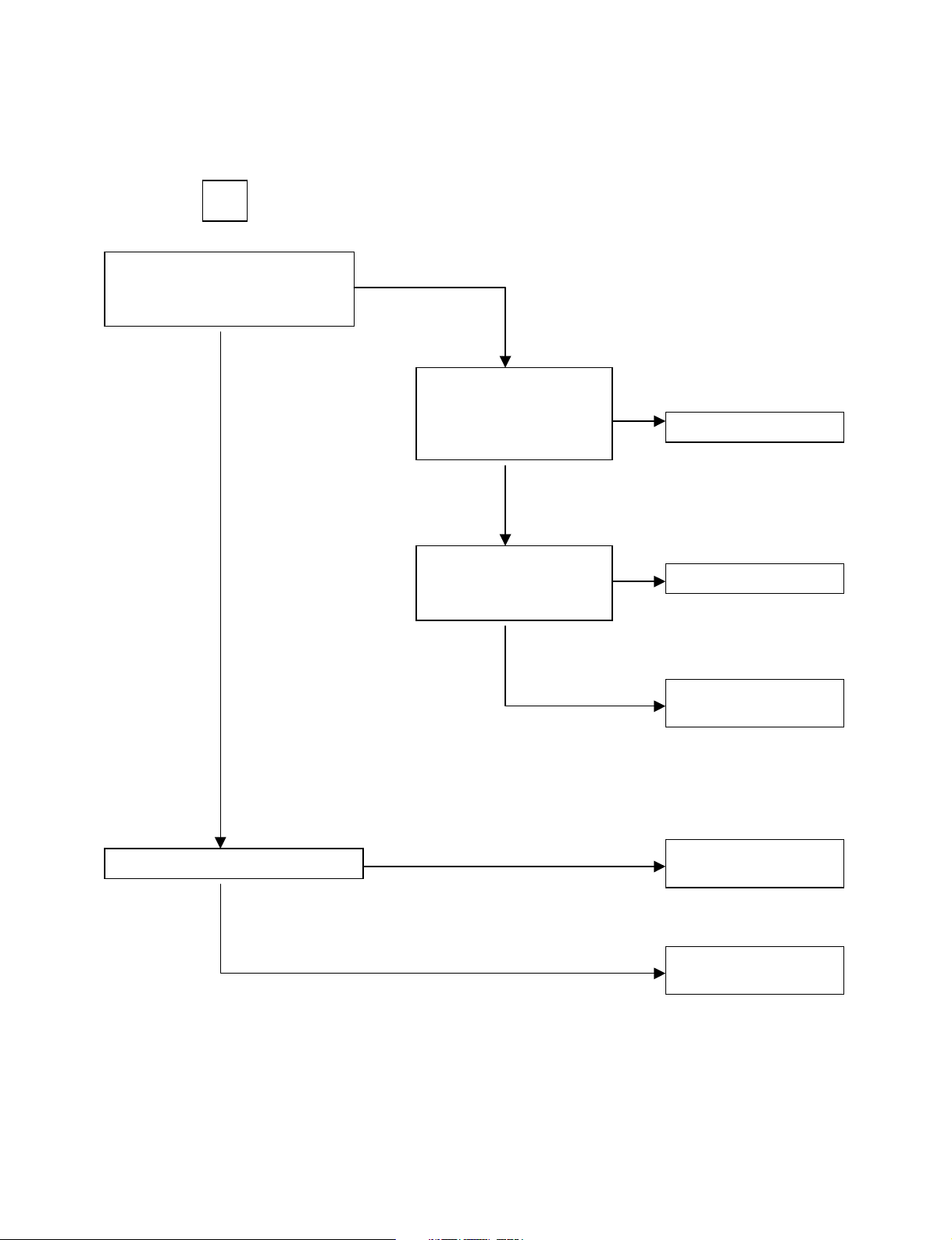
CONNECTOR LOCKING CHECK
(PN808,PN807,PN802,PN801 )
DEFECTIVE CONNECTOR OR
MAIN POWER SUPPLAY
DEFECTIVE IC805
DEFECTIVE MICOM OR
CONNECTOR
DEFECTIVE MICOM OR
CONNECTOR
DEFECTIVE IC801
CHECK VOLTAGE THE PIN 2 OF IC805
IC805 PIN2 : 3.3V
CHECK RESET SIGNAL OF PN807
PN807 PIN12 : 5V
CHECK POWER SUPPLY
PORT( PN808 ,PN807)
PN808 PIN 5 = 6.2V, PIN 7 = 5V
PN807 PIN 1 = 5V
CHECK POWER SUPPLY
PORT( PN808 ,PN807)
PN808 PIN 5 = 6.2V, PIN 7 = 5V
PN807 PIN 1 = 5V
CHECK MICOM INTERFACE
CIRCUIT( PN807 )
PN807 PIN 11,13,14,15 SIGNAL CHECK
(11: STAT, 13: MDATA, 14:MCLK, 15:MLD)
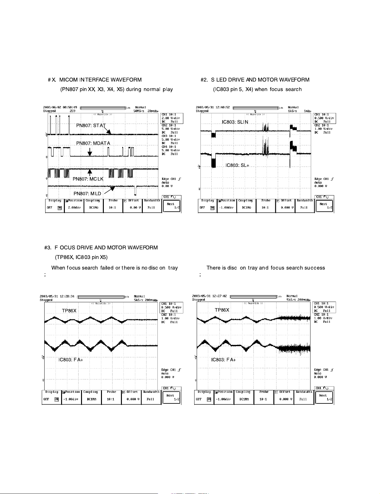
CHECK THE WAVE FORM #1
YES
YES
YES
YES
YES
NO
NO
NO
NO
NO
• “ READING ” DISPLAY CHECK (= ONLY “CD “DISPLAY)
- 2-4 -
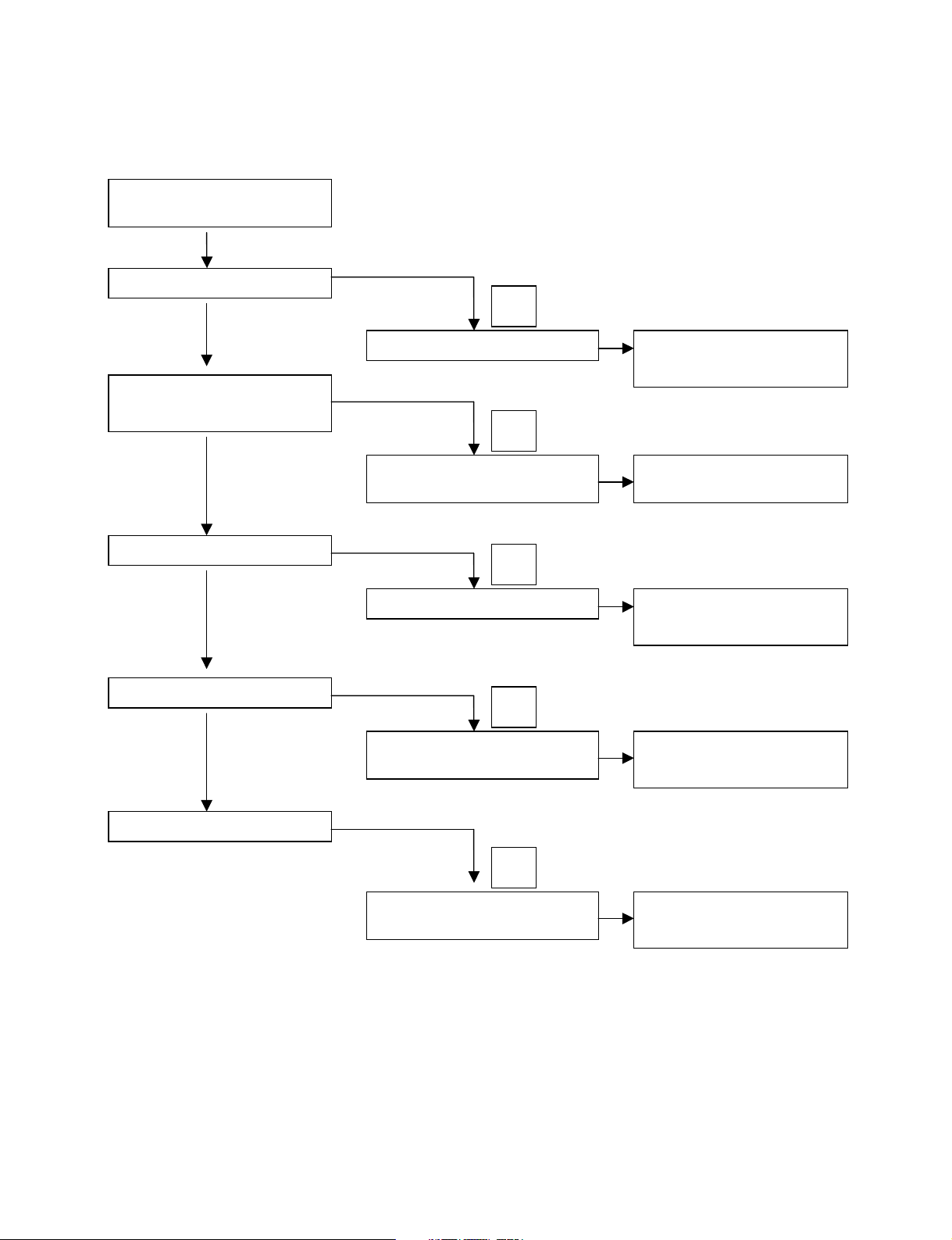
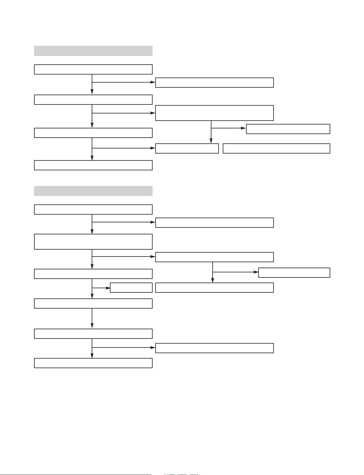
A
B
C
D
E
CONNECTOR LOCKING
CHECK(PN801,PN802)
DOES SLED MOVE ?
CHECK PN802 PIN 3,4( SL+,SL-)
DEFECTIVE PICKUP OR
IC803 OR IC801 OR IC802
DEFECTIVE PICKUP OR
IC803 OR IC801 OR IC802
DEFECTIVE PICKUP OR
IC803 OR IC801
DEFECTIVE PICKUP OR
IC802
DEFECTIVE PICKUP OR
IC803
DEFECTIVE PICKUP OR
IC803 OR IC801 OR IC802
CHECK PN802 PIN 10( LD )
CHECK PN801 PIN 14,15
(TA- ,TA+)
CHECK PN802 PIN
5,6( SP+,SP-)
CHECK PN801 PIN 13,16
( FA-, FA+)
DOES LENSE MOVE ?
(= UP & DOWN)
DOES LASER LIGHT ?
DOES SPINDLE ROTATE ?
IS READING OK ?
YES
YES
YES
YES
YES
NO
NO
NO
NO
NO
• READING OK CHECK (= “NO DISC” DISPLAY)
- 2-5 -
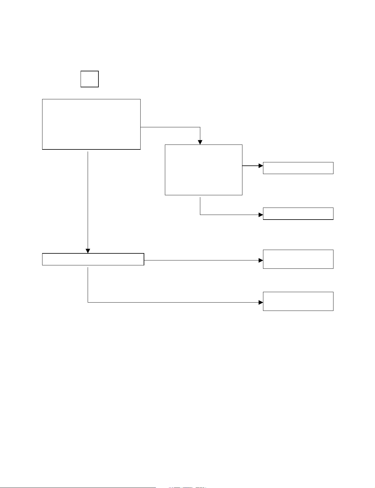
CHECK PN802 CONNECTOR LINE
DEFECTIVE IC801
DEFECTIVE IC803
DEFECTIVE PN802
CONNECTOR
DEFECTIVE PICKUP
SLED MOTOR
A
DOES SL+ WAVEFORM APPEAR AT
( IC803 PIN14 AND PN802 PIN3)
WAVEFORM #2
SLED MOTOR WAVE
DOES SLIN WAVEFORM
APPEAR AT
( IC803 PIN 5)
WAVEFORM #2
SLED DRIVE WAVE
YES
YES
NO
NO
NO
NO
NO
• READING OK CHECK #A (= “NO DISC” DISPLAY)
- 2-6 -
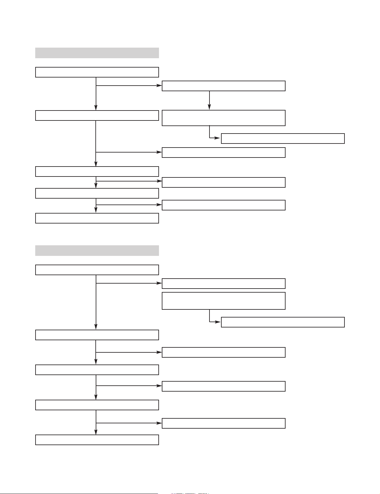
CHECK PN801 CONNECTOR LINE
DEFECTIVE IC801
DEFECTIVE IC803
DEFECTIVE PN801
CONNECTOR
DEFECTIVE PICKUP
FOCUS ACTUATOR
B
DOES FA+ WAVEFORM APPEAR AT
( IC803 PIN15 AND PN801 PIN16)
WAVEFORM #3
FOCUS COIL DRIVE WAVE
DOES FAIN- WAVEFORM
APPEAR AT
( IC803 PIN 26)
WAVEFORM #3
FOCUS DRIVE WAVE
YES
YES
NO
NO
NO
NO
NO
• READING OK CHECK #B (= “NO DISC” DISPLAY)
- 2-7 -
CHECK PN801 CONNECTOR LINE
DEFECTIVE IC805
DEFECTIVE IC802
DEFECTIVE Q801 OR
D811
DEFECTIVE PN801
CONNECTOR
DEFECTIVE PICKUP
LASER PART
C
IS ?V APPLIED TO PIN10 OF
PN801
LASER SUPPLY VOLTAGE CHECK
IS 3.3 V APPLIED TO
PIN3 OF IC802
RF IC SUPPLY VOLTAGE
CHECK
IS 2.0 V PIN2 OF IC802
LASER CONTROL
VOLTAGE CHECK
YES
YES
NO
NO
NO
NO
NO
NO
• READING OK CHECK #C (= “NO DISC” DISPLAY)
- 2-8 -
CHECK PN802 CONNECTOR LINE
DEFECTIVE IC801
DEFECTIVE IC803
DEFECTIVE PN802
CONNECTOR
DEFECTIVE PICKUP
SPINDLE MOTOR
D
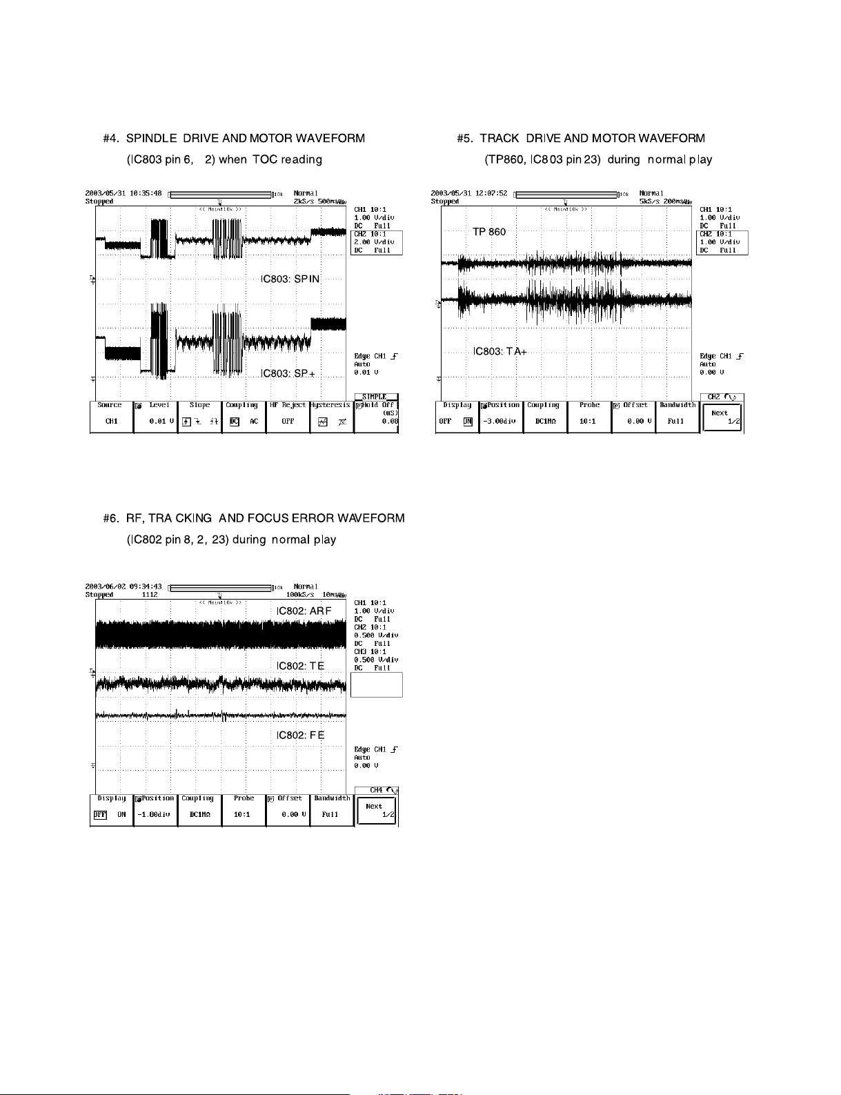
DOES SP+ WAVEFORM APPEAR AT
( IC803 PIN12 AND PN802
PIN6)WAVEFORM #4
SPINDLE MOTOR DRIVE WAVE
DOES SPIN WAVEFORM
APPEAR AT( IC803 PIN 6)
WAVEFORM #4
SPINDLE DRIVE WAVE
YES
YES
NO
NO
NO
NO
• READING OK CHECK #D (= “NO DISC” DISPLAY)
- 2-9 -
CHECK PN802 CONNECTOR LINE
DOES ARF SIGNAL APPEAR?
(IC802 PORT 8)
WAVEFORM #6
DOES FE, TE SIGNAL APPEAR?
(IC802 PORT FE:23, TE:21)
WAVEFORM #6
DEFECTIVE IC801
DEFECTIVE IC803
DEFECTIVE PN802
CONNECTOR
DEFECTIVE PICKUP OR
IC802
DEFECTIVE PICKUP OR
IC802
DEFECTIVE IC801
E
DOES TA+ WAVEFORM APPEAR AT
( IC803 PIN17 AND PN801 PIN15)
WAVEFORM #5
TRACKING COIL DRIVE WAVE
DOES TAIN- WAVEFORM
APPEAR AT
( IC803 PIN 23)
WAVEFORM #5
TRACKING DRIVE WAVE
YES
YES
YES
NO
NO
NO
NO
NO
NO
NO
• READING OK CHECK #E (= “NO DISC” DISPLAY)
- 2-10 -
■ AUDIO PART
P-SENS PART CHECK
ZD 701(+) Voltage check
IC301 26PIN PATTERN Check
Half-wave rectification wave form check
R746 check, then ZD701 replacement
D713 Replacement
VKK CHECK
CN305 4pin DC -33V check
IC301 51PIN check
ZD 700 -33V check
ZD 754 turn on check
Pattern disconnection check
D707, D708 replacement
normal
ZD700 replacement
Refer to power
supply check
C763 -33V and less check
Q754 replacement
- 2-11 -
POWER CHECK
Every kinds of Fuse check
C720(+), C770(-) DC power output check
C725(+), C729(-) DC power output check
IC704, IC705, IC705 power output check
IC704, IC705, IC710 power output check (12V)
IC709 DC5V check
CN513 7PIN 5V check (at CD Function)
normal operation
Fuse replace
CN704 1, 2, 3, 4, 5, 6, 7, 9, 10 AC voltage output check
D713(PBU604) check
Power supply Ass’y check
and transformer replacent
IC301 5V Power output
PN304/CN304 15 PIN check
Check
IC5019BU2090 check & replace
IC501(BU2090) 14PIN HIGH check
Check and replace defective
Power supply Ass’y check
and transformer replacent
CN704, 11, 12 pin AC power output check
IC704, IC705 , IC710 check and replacement
IC301 78PIN 5V check
IC709 replacement
Q904(A1273) Base Low check
Q904, CD Ass’y check replacement
- 2-12 -
Muting circuit Troubleshooting (if MUTE)
Q752(A102) Base “LOW”
C720(+), C770(-) DC power output check
MUTE
c-COM operation status check
Each appropriate TR replacement
Check each function input and operation
status check
Refer to IC601(TDA7429D) IC specification
c-COM check (and CLK/DATA check)
IC705 7812 operation status check (DC12V)
PN701/CN701 connection status check
ZD601 9.1V check
IC601 39PIN (over 8V) check and power
supply circuit check
Q702(A102) operation status check
Q702(A102) Replace if defective
c-COM 2PIN(A-MUTE)
LINE check
No sound
Input check (AUX➞29,36 TUNER➞30,35
TAPE➞28/37 CD➞31/34 PIN)
IC 601 24/25 PIN Output check
IC601 input check (22/21PIN)
IC601 output check (14PIN)
normal
- 2-13 -
Refer to IC202 Troubleshooting
IC501 10 PIN(PB MUTE) operation status check
c-COM 301 10,8 PIN CLK/DATA operation status check
Specific FUNCTION MODE has no sound (TDA7468D)
TAPE
IC202 output check (5,20 PIN)
IC601 36,29 PIN signal input check
IC202 input check (HEAD input) "A"DECK
1,24 "B"DECK 23,2
AUX
JK102 signal input check
IC601 36,29 PIN signal input check
CD
CN603 1,3 PIN signal check and refer to CD Troubleshooting
IC601 34,31 PIN signal input check
TUNER
Refer to TUNERMODULE
IC601 35,30 PIN signal input check
DECK HEAD WIRE connection status check
- 2-14 -
MIC
IC601 function input check
Refer to IC404 Troubleshooting
IC301 Troubleshooting
C301 17, 46, 72, 90 power applied check
IC301 15PIN 5V applied check
X301 oscilates or not
When IC301 11Pin voltage input. High➞Low➞High
IC301 replace
Refer to power supply check
P-SENS terminal check
X301 replace
RESET circuit check
- 2-15 -
IC501,502,302(BU2029) Troubleshooting
IC501 16PIN power applied check
IC501 2, 3 PIN CLK Data check
CONTROL function check
normal
Refer to IC301 Troubleshooting
Refer to power supply check
IC501 replace Pattern check between IC301 and IC501
IC301 3,4 PIN data check
(When switched to CD, TAPE Function)
IC601(TDA7468D) Troubleshooting
IC601 1PIN power applied check
IC601 35,30 Pin waveform output check
IC601 36,29Pin waveform input check
IC601 34,31Pin waveform output check
normal
IC601 21,22 Pulse waveform check
(with tunning VOL DIAL)
Refer to power supply check
IC301 10,8Pin check
IC601 replace
MICOM(10,8) - IC601(21,22) Pattern checkIC601 replace
IC301 Troubleshooting
- 2-16 -
IC701(AMP MODULE) Troubleshooting
AMP ON/OFF check
10,13Pin signal input check
18,5Pin(-), 20, 3Pin(+) Power check
6,17 Pin signal output check
OK
IC502 6PIN operation status check
-9V(IC706) +9(IC710) replace if defective
-9V(IC706) +9(IC710) replace if defective
Refer to Muting circuit
RELAY operation status check (RY703,701)
Refer to power supply check
-9V(IC706) +9(IC710) operation status check
(9,14PIN check)
IC701(AMP MODULE) Troubleshooting
AMP ON/OFF check
9Pin signal input check
12Pin(-), 15Pin(+) voltage check
12 Pin signal output check
OK
IC502 6PIN operation status check
Refer to Muting circuit
Refer to power supply check
RELAY operation status check (RY702)
-9V(IC706) +9(IC710) operation status check
(11,7 PIN check)
- 2-17 -
PLAY check (KIA6289N)
IC202 18Pin VCC power applied
IC202 5,20 Pin signal output check
Muting circuit check
Refer to power supply check
Deck Mecha operation performance check
Deck Mecha replace
IC202 replace
Rec check (Q252, Q202 ON : R273, R223 High)
IC601 33,32 OUT check
IC202 11,14 Pin signal input check
IC202 9,16 Pin output check
IC201 6(12V), 4 Pin High check
L203 2,3PIN oscilation check
Deck replace
Q253, Q203 Base "Low" check
Q253,Q203 replace
Refer to IC203 Troubleshooting
IC202 18Pin VCC voltage check
Voltage check, IC203 Troubleshooting check
C236(+) power supply check
Refer to power supply check
IC203 Troubleshooting check
Q208 replace
L203 replace
Q208 Base 0.6V supplied check
Q208 Collector Low
Q207 replace
normal
- 2-18 -
Dubbing check ("NORMAL or REC"//"HIGH")
Q252,202 "OFF"//"ON" : R273,223 "Low"//"HIGH"
Q253,203 "ON"//"OFF"
Refer to REC Check
IC203 Troubleshooting check
USB IC802(PCM2702)
LM-W5040,3140 applied, LM-W4040,2340 not applied
2, 17, 27 5V voltage check
1.28 12MHz operation status check
IC705 +5V operation check
- 2-19 -
• CD PART WAVEFORMS OF MAJOR CHECK POINT
- 2-20 -
- 2-21 -
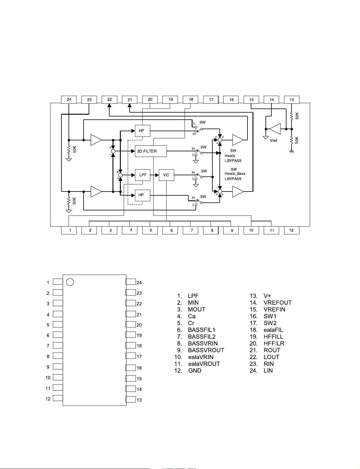
❏ INTERNAL BLOCK DIAGRAM of ICs
• NJM2706 (IC401)
BLOCK DIAGRAM
PIN CONFIGURATION
- 2-22 -
• AF230W20CM (IC701)
BLOCK DIAGRAM
PIN CONFIGURATION
- 2-23 -
• AF310W20CM (IC701)
BLOCK DIAGRAM
PIN CONFIGURATION
PIN DESCRIPTION
Pin Number Symbol Type Description
1 N_DO O NMOS Drain Output
2 VSS G Negative supply Voltage
3 N_CS P NMOS Current Sense Input
4 P_CS P PMOS Current Sense Input
5 AM_F2 O AM Mode control Input 2
6 AM_F1 G AM Mode control Input 1
7 VEE I Negative supply Voltage
8 STANDBY I ON/OFF control
9 IN P Audio Input
10 P_STATE I Protection State
11 VCC I Positive supply Voltage
12 OUT O Audio Output
13 GND I Signal Ground
14 SUBGND P Sub Ground
15 VDD I Positive supply Voltage
16 P_DO O PMOS Drain Output
- 2-24 -
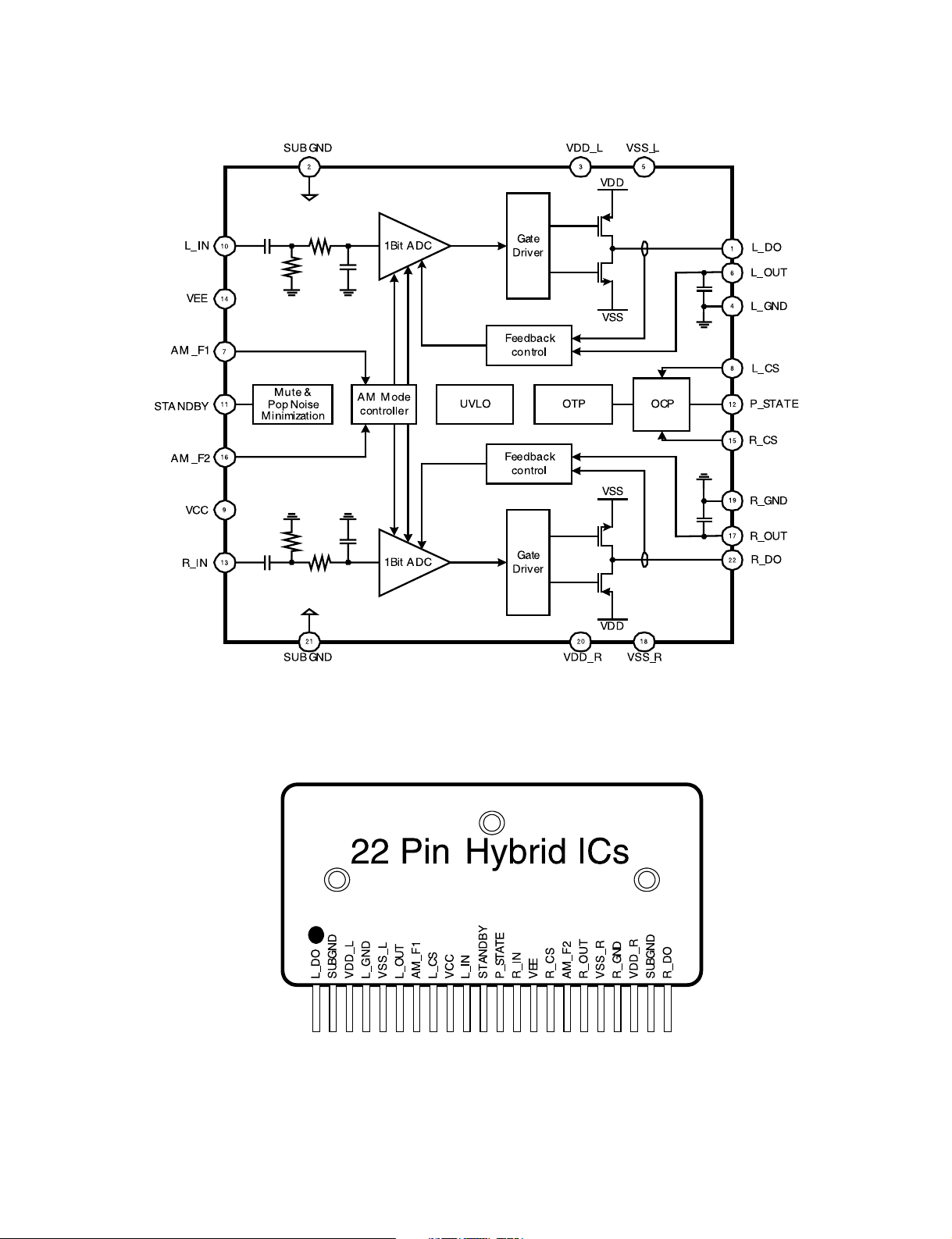
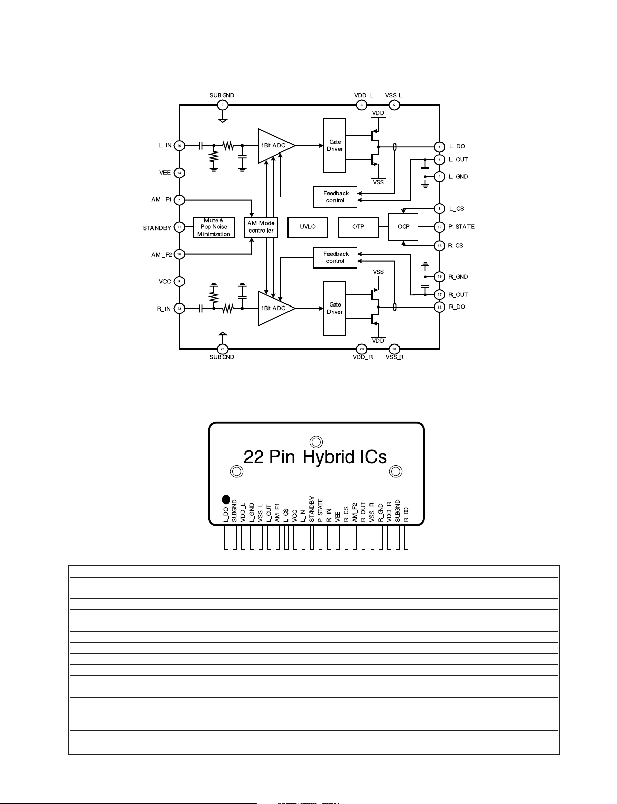
PIN DESCRIPTION
Pin Number Symbol Type Description
1 L_DO O L-Channel Drain Output
2 SUBGND G Sub Ground
3 VDD_L P L-Channel Positive supply Voltage
4 L_GND P L-Channel Signal Ground
5 VSS_L O L-Channel Negative supply Voltage
6 L_OUT G L-Channel Audio Output
7 AM_F1 I AM Mode control Input 1
8 L_CS I L-Channel Current Sense Input
9 VCC P Positive supply Voltage
10 L_IN I L-Channel Audio Input
11 STANDBY I ON/OFF control
12 P_STATE O Protection State
13 R_IN I R-Channel Audio Input
14 VEE P Negative supply Voltage
15 R_CS I R-Channel Current Sense Input
16 AM_F2 I AM Mode control Input 2
17 R_OUT G R-Channel Audio Output
18 VSS_R O R-Channel Negative supply Voltage
19 R_GND P R-Channel Signal Ground
20 VDD_R P R-Channel Positive supply Voltage
21 SUBGND G Sub Ground
22 R_DO O R-Channel Drain Output
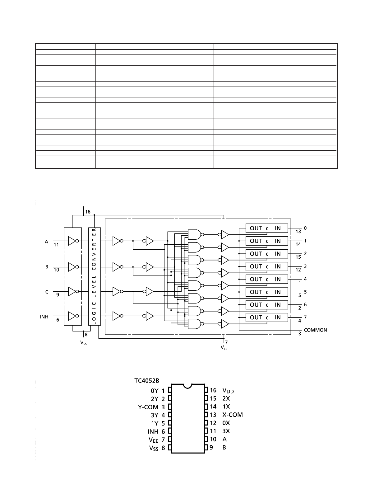
• TC4052BP (IC801)
BLOCK DIAGRAM
PIN ASSIGNMENT
❏ BLOCK DIAGRAM
2-25 2-26
2-27 2-28
❏ SCHEMATIC DIAGRAM
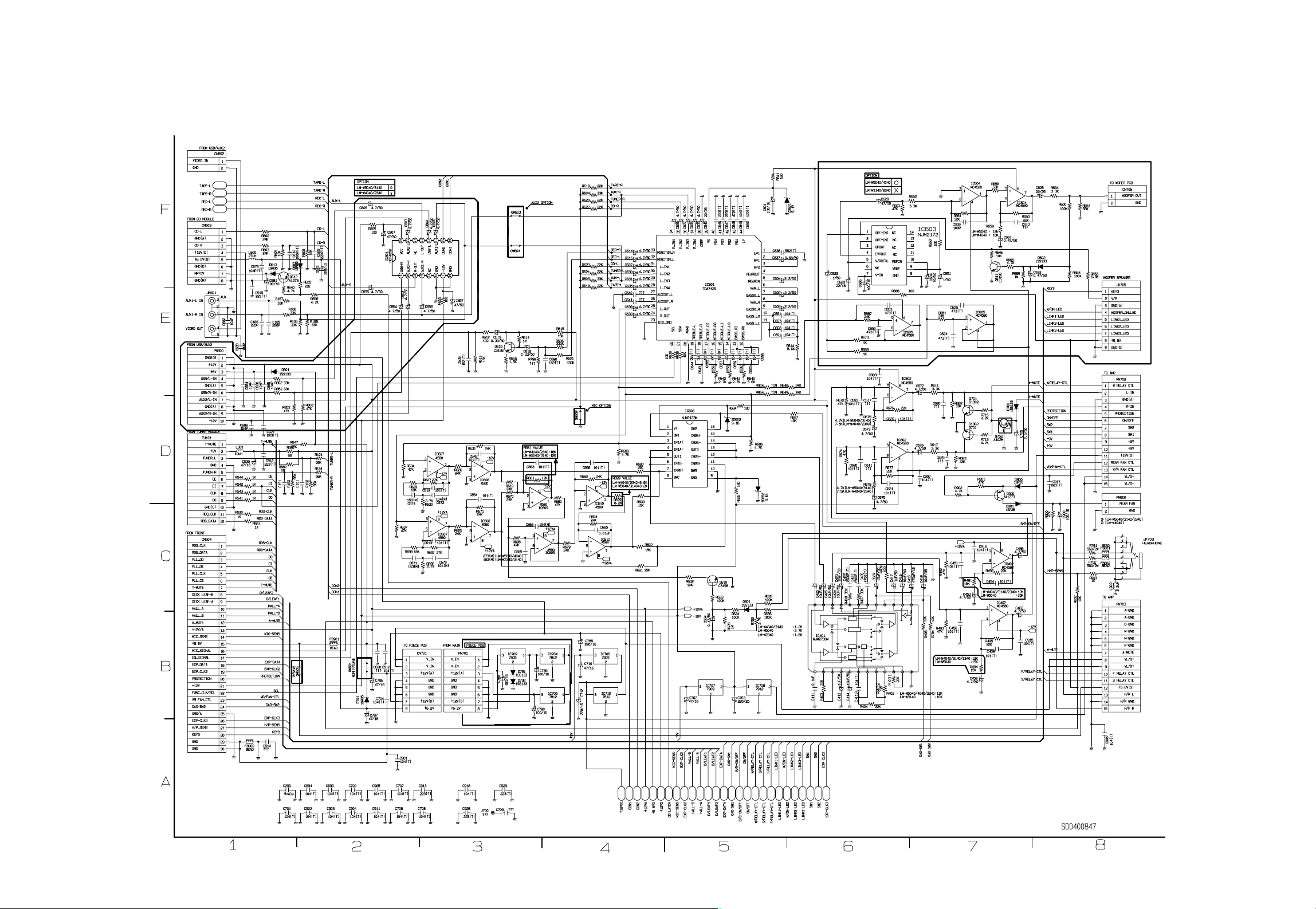
• MAIN SCHEMATIC DIAGRAM

2-29 2-30
• DECK SCHEMATIC DIAGRAM

2-31 2-32
• AUDIO/WOOFER AMP, POWER SCHEMATIC DIAGRAM

2-33 2-34
• FRONT, MIC SCHEMATIC DIAGRAM

2-35 2-36
• USB & AV, WOOFER SCHEMATIC DIAGRAM

2-37 2-38
• CDP SCHEMATIC DIAGRAM

2-39 2-40
❏ WIRING DIAGRAMS

2-41 2-42
❏ PRINTED CIRCUIT DIAGRAMS
• MAIN P.C. BOARD (SOLDER SIDE)

2-43 2-44
• MAIN P.C. BOARD (COMPONENT SIDE)

2-45 2-46
• FRONT P.C. BOARD (SOLDER SIDE)

2-47 2-48
• FRONT P.C. BOARD (COMPONENT SIDE)

2-49 2-50
• POWER, MIC, WOOFER P.C. BOARD (COMPONENT SIDE)

2-51 2-52
• POWER, MIC, WOOFER P.C. BOARD (SOLDER SIDE)

2-53 2-54
• AMP, USB & AV P.C. BOARD (COMPONENT SIDE)

2-55 2-56
• AMP, USB & AV P.C. BOARD (SOLDER SIDE)

2-57 2-58
• CDP P.C. BOARD (SOLDER SIDE) • CDP P.C. BOARD (COMPONENT SIDE)

3-1 3-2
SECTION 3. EXPLODED VIEWS
A26
300
450
301
290
266
267
268
272
269
270
275
A49
274
276
452
262
261
258
254
255
263
265
278
273
253
251
250
252
288
259
264
257
277
260
256
285
271
A41
451
283
284
A47
302
286
A48
305
285
281
282
A43
A00
280
A46
NOTE) Refer to “SECTION 5 REPLACEMENT
PARTS LIST” in order to look for the
part number of each part.
• CABINET AND MAIN FRAME SECTION

3-3 3-4
• TAPE DECK MECHANISM (A/R & A/S : LEFT A/S DECK)
016
401
018
007
008
015
023
019
021
020
505
017
403
504
025
026
030
029
028
401
027
502
009
401
003
501
401
011
013
009
022
LOCA. NO. LG PART NO. DESCRIPTION SPECIFICATION
A00 6720AG0002C DECK,AUDIO CWM42FR47 TOKYO PIGEON L-DOUBL
003 6768R-PP03A DECK MECHANISM PARTS 33-160-4309 PIGEON PRESS CASSE
007 6768R-GP03B DECK MECHANISM PARTS 50-222-4578 PIGEON GEAR IDLER
008 6768R-SP01F DECK MECHANISM PARTS 01-082-4598 PIGEON SPRING CWL4
009 6768R-MP01C DECK MECHANISM PARTS 50-219-4014 PIGEON MOLD CWL44
011 6768R-SP01A DECK MECHANISM PARTS 01-081-4601 PIGEON SPRING CWL4
013 6768R-SP03A DECK MECHANISM PARTS 01-082-4686 PIGEON SPRING CRM4
015 6768R-AP01A DECK MECHANISM PARTS 50-268-3016 PIGEON ARM CWL44
016 6768R-GP01H DECK MECHANISM PARTS 50-093-4503 PIGEON GEAR CRL442
017 6768R-AP01C DECK MECHANISM PARTS 50-239-4072 PIGEON ARM CWL44
018 6768R-GP01J DECK MECHANISM PARTS 50-222-4428 PIGEON GEAR CRL442
019 6768R-SP01P DECK MECHANISM PARTS 01-081-4678 PIGEON SPRING CRL4
020 6768R-BP01C DECK MECHANISM PARTS 02-083-4188 PIGEON BELT/FELT C
021 6768R-LP01C DECK MECHANISM PARTS 50-223-4429 PIGEON PULLEY/FLYW
022 6768R-VP03A DECK MECHANISM PARTS 50-093-4748 PIGEON SOLENOID AS
023 6768R-GP03A DECK MECHANISM PARTS 50-093-4810 PIGEON GEAR ASSY C
025 6768R-JP03B DECK MECHANISM PARTS 50-093-31009 PIGEON PULLEY/FLY
026 6768R-SP01D DECK MECHANISM PARTS 01-080-4609 PIGEON SPRING CWL4
027 6768R-DP01A DECK MECHANISM PARTS 50-259-3342 PIGEON LEVER CWL44
028 6768R-RP01A DECK MECHANISM PARTS 22-027-41054 PIGEON ROLLER CWL
029 6768R-MP01A DECK MECHANISM PARTS 50-219-4033 PIGEON MOLD CWL44
030 6768R-EP03C DECK MECHANISM PARTS T21V0P PIGEON HEAD CWM42FF30
401 6768R-CP01B DECK MECHANISM PARTS GSE20A2005 PIGEON SCREW CWL44
403 6768R-CP01D DECK MECHANISM PARTS GSL10A1704 PIGEON SCREW CWL44
501 6768R-WP03A DECK MECHANISM PARTS GWN19S035040 PIGEON WASHER CRM
502 6768R-WP03B DECK MECHANISM PARTS 03-000-4532 PIGEON WASHER CRM4
504 6768R-WP01D DECK MECHANISM PARTS GWP21X045020 PIGEON WASHER CWL
505 6768R-WP01E DECK MECHANISM PARTS GWP12X030040S PIGEON WASHER CW

3-5 3-6
• TAPE DECK MECHANISM (A/R & A/S : RIGHT A/R DECK)
025
504
023
015
022
019
037
021
020
505
018
017
016
506
006
A01
402
008
007
401
001
002
003
502
507
501
502
402
401
009
401
009
011
013
035
039
031
040
028
029
027
026
038
028
032
406
409
403
036
LOCA. NO. LG PART NO. DESCRIPTION SPECIFICATION
A00 6720AG0002C DECK,AUDIO CWM42FR47 TOKYO PIGEON L-DOUBL
A01 6768R-UP03D DECK MECHANISM PARTS 50-093-4895 PIGEON PWB UNIT CW
001 6768R-BP03D DECK MECHANISM PARTS 02-083-4254 PIGEON BELT/FELT C
002 6768R-BP03E DECK MECHANISM PARTS 02-083-4256 PIGEON BELT/FELT C
003 6768R-PP03A DECK MECHANISM PARTS 33-160-4309 PIGEON PRESS CASSE
006 6768R-QP03C DECK MECHANISM PARTS 50-093-4880 PIGEON MOTOR(ASSY)
007 6768R-GP03B DECK MECHANISM PARTS 50-222-4578 PIGEON GEAR IDLER
008 6768R-SP01F DECK MECHANISM PARTS 01-082-4598 PIGEON SPRING CWL4
009 6768R-MP01C DECK MECHANISM PARTS 50-219-4014 PIGEON MOLD CWL44
011 6768R-SP01A DECK MECHANISM PARTS 01-081-4601 PIGEON SPRING CWL4
013 6768R-SP03A DECK MECHANISM PARTS 01-082-4686 PIGEON SPRING CRM4
015 6768R-AP01A DECK MECHANISM PARTS 50-268-3016 PIGEON ARM CWL44
016 6768R-GP01H DECK MECHANISM PARTS 50-093-4503 PIGEON GEAR CRL442
017 6768R-AP01C DECK MECHANISM PARTS 50-239-4072 PIGEON ARM CWL44
018 6768R-GP01J DECK MECHANISM PARTS 50-222-4428 PIGEON GEAR CRL442
019 6768R-SP01P DECK MECHANISM PARTS 01-081-4678 PIGEON SPRING CRL4
020 6768R-BP01C DECK MECHANISM PARTS 02-083-4188 PIGEON BELT/FELT C
021 6768R-LP01C DECK MECHANISM PARTS 50-223-4429 PIGEON PULLEY/FLYW
022 6768R-VP03A DECK MECHANISM PARTS 50-093-4748 PIGEON SOLENOID AS
023 6768R-GP03A DECK MECHANISM PARTS 50-093-4810 PIGEON GEAR ASSY C
025 6768R-JP03B DECK MECHANISM PARTS 50-093-31009 PIGEON PULLEY/FLY
026 6768R-SP01D DECK MECHANISM PARTS 01-080-4609 PIGEON SPRING CWL4
027 6768R-DP01A DECK MECHANISM PARTS 50-259-3342 PIGEON LEVER CWL44
028 6768R-RP01A DECK MECHANISM PARTS 22-027-41054 PIGEON ROLLER CWL
029 6768R-MP01A DECK MECHANISM PARTS 50-219-4033 PIGEON MOLD CWL44
031 6768R-SP04A DECK MECHANISM PARTS 01-082-4731 PIGEON SPRING
032 6768R-EP04A DECK MECHANISM PARTS 50-093-41007 PIGEON HEAD ASSY
035 6768R-PP04A DECK MECHANISM PARTS 50-119-4915 PIGEON PRESS
036 6768R-SP04B DECK MECHANISM PARTS 01-081-4730 PIGEON SPRING
037 6768R-JP03A DECK MECHANISM PARTS 50-093-4674 PIGEON PULLEY/FLYW
038 6768R-MP01D DECK MECHANISM PARTS 50-219-4034 PIGEON MOLD CWL44
039 6768R-MP02A DECK MECHANISM PARTS 50-219-3900 PIGEON MOLD
040 6768R-SP01M DECK MECHANISM PARTS 01-080-4607 PIGEON SPRING CWL4
401 6768R-CP01B DECK MECHANISM PARTS GSE20A2005 PIGEON SCREW CWL44
402 6768R-CP01A DECK MECHANISM PARTS GSE10A2003 PIGEON SCREW CWL44
403 6768R-CP01D DECK MECHANISM PARTS GSL10A1704 PIGEON SCREW CWL44
406 6768R-CP01G DECK MECHANISM PARTS GSE20A2004 PIGEON SCREW CWL44
409 6768R-CP02A DECK MECHANISM PARTS GSD10A2016 PIGEON SCREW
501 6768R-WP03A DECK MECHANISM PARTS GWN19S035040 PIGEON WASHER CRM
502 6768R-WP03B DECK MECHANISM PARTS 03-000-4532 PIGEON WASHER CRM4
504 6768R-WP01D DECK MECHANISM PARTS GWP21X045020 PIGEON WASHER CWL
505 6768R-WP01E DECK MECHANISM PARTS GWP12X030040S PIGEON WASHER CW
506 6768R-WP01H DECK MECHANISM PARTS GWP23X040020 PIGEON WASHER CWL
507 6768R-WP01F DECK MECHANISM PARTS GWN21X040040 PIGEON WASHER CWL

3-7 3-8
• CD MECHANISM
416
151
156
418
169
173
171
170
419
163
422
165
159
164
417
417
416
166
167
177
175
172
162
153
168
155
LOCA.NO. PART NO DESCRIPTION SPECIFICATION
A26 4405RBE004C MECHANISM ASSEMBLY CDM-H1503 3 CD CHANGER
A30 3041RB0002C BASE ASSEMBLY PU(SPRING DAMPER)
A35 6717RCA001A PICK UP ASSY KSM-213VSCM SONY FRONT LOADING
151 3390RB0002A TRAY DISC(CDM-H1503)
153 4470RB0005A GEAR TRAY (CDM-H1503)
155 4681RBA001A MOTOR ASSEMBLY TRAY (CDM-H1503)
156 6871RF9211A PWB(PCB) ASSEMBLY,FRONT 1503 T/D SENSOR
159 3390RB0001A TRAY LOADING(CDM-H1503)
162 4400SB0001A BELT MAIN(CDM-H1303)
163 4470SB0003A GEAR PULLEY (CDM-H1303)
164 4470RB0003A GEAR LOADING (CDM-H1503)
165 6871RZ7036A PWB(PCB) ASSEMBLY,OTHERS CDM-H1503 UP/DW/OP/CL
166 4470RB0006A GEAR PU UP (CDM-H1503)
167 4470RB0007A GEAR PU DOWN (CDM-H1503)
168 4470RB0002A GEAR CAM (CDM-H1503)
169 4860SB0001A CLAMP DISC(CDM-H1303)
170 3550SB0001A COVER MAGNET(CDM-H1303)
171 524-012AAAA COVER CLAMP MAGNET (030X018X5T)
172 3040RB0005A BASE MAIN (CDM-H1503)
173 4510RB0001A LEVER S/W CLOSE
175 4680SBP001A MOTOR(MECH) OTHER . . .
177 4470RB0001A GEAR MAIN (CDM-H1503)
184 4900RB0001A DAMPER RUBBER 3CD CHANGER
185 3040SB0003A BASE PU(CDM-H1303)
186 4970RB0001A SPRING COIL 3 CD CHANGER
187 4970RB0001B SPRING COIL 50 3CD CHANGER
416 88H-0004 CD MECHA PARTS 3X12X12FNM
417 88H-0002 CD MECHA PARTS 3X9X12FZMY
418 353-025BAAA SCREW #NAME?
419 88H-0003 CD MECHA PARTS 3X12X10FZMY
420 353S353F SCREW #NAME?
421 6756SBX001A CD MECHANISM PARTS SCREW 2.6X10X10XFZMY CDM-H813
422 353-028H SCREW #NAME?


- 4-1 -
SECTION 4. SPEAKER PART
839
841
840
836
831
837
838
830
827
829
820
821
826
825
827
822
823
824
834
833
832
828
(LEFT)
(LEFT)
(LEFT)
(RIGHT)
(RIGHT)
(RIGHT)
❏ LMS-W2340
LCOA.NO PART NO. DESCRIPTION SPECIFICATION
820 3720RMF095A PANEL,FRONT SPK LMS-W5040 MOLD LEFT LMS-W4
821 3720RMF095B PANEL,FRONT SPK LMS-W5040 MOLD RIGHT LMS-W
822 6400WETK01A SPEAKER,WOOFER 20LD5EHC3500O EAW WOOFER 6OHM
823 353M050N SCREW,DRAWING + 1 D3.5 L14.0 FZMY2 FBK
824 353M051S SCREW,DRAWING H1 D3.5 L18 SWRCH16A/CR LMS-W5
825 5208RM0055A DUCT SPK LMS-W5040 MOLD LMS-W5040/W
826 5208RM0055B DUCT SPK LMS-W5040/W4040/W3140/W234
827 353M051P SCREW,DRAWING + 1 D3.0 L8.0 MSWR3/FZW SILVER
828 6400METC01A SPEAKER,WOOFER 08R60EHC3492D EAW MID-RANGE 12
829 4766RM0099A FELT UNIDENTIFY BLACK 3 INCH WOOFER
830 6400TETA01A SPEAKER,TWEETER 05N45EHC3489B EAW TWEETER(CONE
831 4766RM0100A FELT LMS-W5040 BLACK 2 INCH TWEETER
832 4766RM0098A FELT UNIDENTIFY BLACK 8 INCH WOOFER
833 6871RU0035A PWB(PCB) ASSEMBLY,SUBSET(AUDIO LMS-W5040 STANDARD 1.0MF POSSI
834 353M025Q SCREW,DRAWING WOOD,3X10 FBK
836 3610RM0005A FOOT EVA PHI 20 X 2T FE-986/886E ST
837 4760RM0077A BAFFLE SPK LMS-W5040 MOLD LEFT LMS-W4
838 4760RM0077B BAFFLE SPK LMS-W5040 MOLD RIGHT LMS-W
839 3091RMW129A CABINET ASSEMBLY SPK LMS-W5040 CABINET ASSY PB
840 6871RU0012A PWB(PCB) ASSEMBLY,SUBSET(AUDIO LMS-W5040 NET WORK ASSY STANDA
841 1WZZRM0003A WASHER,DRAWING SPK LMS-W5040 PRESS WASHER 8 X

- 4-2 -

Sales Model
Numero de localizacion
Numero de Parte
Fecha Parte Comienza a Ser Usada
N?ero de Parte/B
6768R-BP03D
DECK MECHANISM PARTS
6768R-BP03D
DECK MECHANISM PARTS
6768R-BP03E
DECK MECHANISM PARTS
6768R-BP03E
DECK MECHANISM PARTS
6768R-PP03A
DECK MECHANISM PARTS
6768R-PP03A
DECK MECHANISM PARTS
6768R-QP03C
DECK MECHANISM PARTS
6768R-QP03C
DECK MECHANISM PARTS
6768R-QP03C
DECK MECHANISM PARTS
6768R-GP03B
DECK MECHANISM PARTS
6768R-GP03B
DECK MECHANISM PARTS
6768R-SP01F
DECK MECHANISM PARTS
6768R-SP01F
DECK MECHANISM PARTS
6768R-SP01F
DECK MECHANISM PARTS
6768R-MP01C
DECK MECHANISM PARTS
6768R-MP01C
DECK MECHANISM PARTS
6768R-MP01C
DECK MECHANISM PARTS
6768R-SP01A
DECK MECHANISM PARTS
6768R-SP01A
DECK MECHANISM PARTS
6768R-SP01A
DECK MECHANISM PARTS
6768R-SP03A
DECK MECHANISM PARTS
6768R-SP03A
DECK MECHANISM PARTS
6768R-AP01A
DECK MECHANISM PARTS
6768R-AP01A
DECK MECHANISM PARTS
6768R-AP01A
DECK MECHANISM PARTS
6768R-GP01H
DECK MECHANISM PARTS
6768R-GP01H
DECK MECHANISM PARTS
6768R-GP01H
DECK MECHANISM PARTS
6768R-AP01C
DECK MECHANISM PARTS
6768R-AP01C
DECK MECHANISM PARTS
6768R-AP01C
DECK MECHANISM PARTS
6768R-GP01J
DECK MECHANISM PARTS
6768R-GP01J
DECK MECHANISM PARTS
Fecha Final Descripcion C?igo Alterno
1
1
2
2
3
3
6
6
6
7
7
8
8
8
9
9
9
11
11
11
13
13
15
15
15
16
16
16
17
17
17
18
18
3/16/2004
3/16/2004
3/16/2004
3/16/2004
3/16/2004
3/16/2004
3/16/2004
3/16/2004
3/16/2004
3/16/2004
3/16/2004
3/16/2004
3/16/2004
3/16/2004
3/16/2004
3/16/2004
3/16/2004
3/16/2004
3/16/2004
3/16/2004
3/16/2004
3/16/2004
3/16/2004
3/16/2004
3/16/2004
3/16/2004
3/16/2004
3/16/2004
3/16/2004
3/16/2004
3/16/2004
3/16/2004
3/16/2004
R
R
R
R
R
R
R
R
R
R
R
R
R
R
R
R
R
R
R
R
R
R
R
R
R
R
R
R
R
R
R
R
R

18
6768R-GP01J
DECK MECHANISM PARTS
6768R-SP01P
DECK MECHANISM PARTS
6768R-SP01P
DECK MECHANISM PARTS
6768R-BP01C
DECK MECHANISM PARTS
6768R-BP01C
DECK MECHANISM PARTS
6768R-BP01C
DECK MECHANISM PARTS
6768R-LP01C
DECK MECHANISM PARTS
6768R-LP01C
DECK MECHANISM PARTS
6768R-LP01C
DECK MECHANISM PARTS
6768R-VP03A
DECK MECHANISM PARTS
6768R-VP03A
DECK MECHANISM PARTS
6768R-GP03A
DECK MECHANISM PARTS
6768R-GP03A
DECK MECHANISM PARTS
6768R-GP03A
DECK MECHANISM PARTS
6768R-JP03B
DECK MECHANISM PARTS
6768R-JP03B
DECK MECHANISM PARTS
6768R-SP01D
DECK MECHANISM PARTS
6768R-SP01D
DECK MECHANISM PARTS
6768R-SP01D
DECK MECHANISM PARTS
6768R-DP01A
DECK MECHANISM PARTS
6768R-DP01A
DECK MECHANISM PARTS
6768R-DP01A
DECK MECHANISM PARTS
6768R-RP01A
DECK MECHANISM PARTS
6768R-RP01A
DECK MECHANISM PARTS
6768R-RP01A
DECK MECHANISM PARTS
6768R-MP01A
DECK MECHANISM PARTS
6768R-MP01A
DECK MECHANISM PARTS
6768R-MP01A
DECK MECHANISM PARTS
6768R-EP03C
DECK MECHANISM PARTS
6768R-EP03C
DECK MECHANISM PARTS
6768R-SP04A
DECK MECHANISM PARTS
6768R-SP04A
DECK MECHANISM PARTS
6768R-EP04A
DECK MECHANISM PARTS
6768R-EP04A
DECK MECHANISM PARTS
6768R-EP04A
DECK MECHANISM PARTS
6768R-PP04A
DECK MECHANISM PARTS
6768R-PP04A
DECK MECHANISM PARTS
19
19
20
20
20
21
21
21
22
22
23
23
23
25
25
26
26
26
27
27
27
28
28
28
29
29
29
30
30
31
31
32
32
32
35
35
3/16/2004
3/16/2004
3/16/2004
3/16/2004
3/16/2004
3/16/2004
3/16/2004
3/16/2004
3/16/2004
3/16/2004
3/16/2004
3/16/2004
3/16/2004
3/16/2004
3/16/2004
3/16/2004
3/16/2004
3/16/2004
3/16/2004
3/16/2004
3/16/2004
3/16/2004
3/16/2004
3/16/2004
3/16/2004
3/16/2004
3/16/2004
3/16/2004
3/16/2004
3/16/2004
3/16/2004
3/16/2004
3/16/2004
3/16/2004
3/16/2004
3/16/2004
3/16/2004
R
R
R
R
R
R
R
R
R
R
R
R
R
R
R
R
R
R
R
R
R
R
R
R
R
R
R
R
R
R
R
R
R
R
R
R
R

36
6768R-SP04B
DECK MECHANISM PARTS
6768R-SP04B
DECK MECHANISM PARTS
6768R-JP03A
DECK MECHANISM PARTS
6768R-JP03A
DECK MECHANISM PARTS
6768R-MP01D
DECK MECHANISM PARTS
6768R-MP01D
DECK MECHANISM PARTS
6768R-MP01D
DECK MECHANISM PARTS
6768R-MP02A
DECK MECHANISM PARTS
6768R-MP02A
DECK MECHANISM PARTS
6768R-SP01M
DECK MECHANISM PARTS
6768R-SP01M
DECK MECHANISM PARTS
6768R-SP01M
DECK MECHANISM PARTS
3390RB0002A
3390RB0002A
4470RB0005A
4470RB0005A
4470RB0005A
4681RBA001A
MOTOR ASSEMBLY
4681RBA001A
MOTOR ASSEMBLY
4681RBA001A
MOTOR ASSEMBLY
4681RBA001B
MOTOR ASSEMBLY
4681RBA001B
MOTOR ASSEMBLY
4681RBA001B
MOTOR ASSEMBLY
6871RF9211A
PWB(PCB) ASSEMBLY,FR
6871RF9211A
PWB(PCB) ASSEMBLY,FR
6871RF9211A
PWB(PCB) ASSEMBLY,FR
3390RB0001A
3390RB0001A
3390RB0001A
4400SB0001A
4400SB0001A
4400SB0001A
4470SB0003A
4470SB0003A
4470SB0003A
4470RB0003A
4470RB0003A
36
37
37
38
38
38
39
39
40
40
40
151
151
153
153
153
155
155
155
155
155
155
156
156
156
159
159
159
162
162
162
163
163
163
164
164
3/16/2004
3/16/2004
3/16/2004
3/16/2004
3/16/2004
3/16/2004
3/16/2004
3/16/2004
3/16/2004
3/16/2004
3/16/2004
3/16/2004
7/2/2002 TRAY R
7/2/2002 TRAY R
7/2/2002 GEAR R
7/2/2002 GEAR R
7/2/2002 GEAR R
6/23/2004
6/23/2004
6/23/2004
6/23/2004
6/23/2004
6/23/2004
7/2/2002
7/2/2002
7/2/2002
7/2/2002 TRAY R
7/2/2002 TRAY R
7/2/2002 TRAY R
12/2/2002 BELT R
12/2/2002 BELT R
12/2/2002 BELT R
12/2/2002 GEAR R
12/2/2002 GEAR R
12/2/2002 GEAR R
12/2/2002 GEAR R
12/2/2002 GEAR R
R
R
R
R
R
R
R
R
R
R
R
R
R
R
R
R
R
R
R
R
R

164
4470RB0003A
6871RZ7036A
PWB(PCB) ASSEMBLY,OT
6871RZ7036A
PWB(PCB) ASSEMBLY,OT
6871RZ7036A
PWB(PCB) ASSEMBLY,OT
4470RB0006A
4470RB0006A
4470RB0006A
4470RB0007A
4470RB0007A
4470RB0007A
4470RB0002A
4470RB0002A
4470RB0002A
4860RB0002B
4860RB0002B
3040RB0005A
3040RB0005A
3040RB0005A
4510RB0001A
4510RB0001A
4510RB0001A
4680SBP001A
MOTOR(MECH)
4680SBP001A
MOTOR(MECH)
4680SBP001A
MOTOR(MECH)
4470RB0001A
4470RB0001A
4470RB0001A
4900RB0001A
4900RB0001A
4900RB0001A
3040SB0003A
3040SB0003A
3040SB0003A
4970RB0001A
4970RB0001A
4970RB0001B
4970RB0001B
165
165
165
166
166
166
167
167
167
168
168
168
169
169
172
172
172
173
173
173
175
175
175
177
177
177
184
184
184
185
185
185
186
186
187
187
12/2/2002 GEAR R
3/6/2003
3/6/2003
3/6/2003
12/2/2002 GEAR R
12/2/2002 GEAR R
12/2/2002 GEAR R
12/2/2002 GEAR R
12/2/2002 GEAR R
12/2/2002 GEAR R
12/2/2002 GEAR R
12/2/2002 GEAR R
12/2/2002 GEAR R
7/7/2004 CLAMP R
7/7/2004 CLAMP R
12/2/2002 BASE R
12/2/2002 BASE R
12/2/2002 BASE R
12/2/2002 LEVER R
12/2/2002 LEVER R
12/2/2002 LEVER R
12/2/2002
12/2/2002
12/2/2002
12/2/2002 GEAR R
12/2/2002 GEAR R
12/2/2002 GEAR R
4/25/2002 DAMPER R
4/25/2002 DAMPER R
4/25/2002 DAMPER R
4/25/2002 BASE R
4/25/2002 BASE R
4/25/2002 BASE R
4/25/2002 SPRING R
4/25/2002 SPRING R
4/25/2002 SPRING R
4/25/2002 SPRING R
R
R
R
R
R
R

250
3790RCD039A
WINDOW,DECO
3790RCD039B
WINDOW,DECO
3550RC0419C
3550RC0419B
4940RCV064A
3508RCH036A
DECORATION
4940RCZ010A
4940RCZ011A
3508RCH035A
DECORATION
3550RC0418A
3790RCP102A
WINDOW,DECO
3550RC0417A
4930RC0105A
4930RC0105B
4940S-6770G
4940S-6770G
4940RCT257A
4940RCT259A
4940RCT260A
4940RCT255A
4930RC0106A
4940RCT254A
4901R-0002C
DAMPER ASSEMBLY
4901R-0002C
DAMPER ASSEMBLY
4901R-0002C
DAMPER ASSEMBLY
4974R-0042B
4974R-0042B
4974R-0042B
3858RCX065A
SHEET (MECH)
4974R-0041B
4974R-0041B
4974R-0041B
3720RCF168D
PANEL,FRONT
3140RCH020A
251
252
253
254
255
256
257
258
260
261
262
263
264
265
265
266
267
268
269
270
271
273
273
273
274
274
274
275 442-085E 4/28/2004 SPRING R
275 442-085E 4/28/2004 SPRING R
275 442-085E 4/28/2004 SPRING R
276
277
277
277
278
280
4/28/2004
4/28/2004
4/28/2004 COVER R
4/28/2004 COVER R
4/28/2004 KNOB R
4/28/2004
4/28/2004 KNOB R
5/7/2004 KNOB R
4/28/2004
4/28/2004 COVER R
4/28/2004
4/28/2004 COVER R
4/28/2004 HOLDER R
4/28/2004 HOLDER R
4/28/2004 KNOB R
4/28/2004 KNOB R
4/28/2004 KNOB R
4/28/2004 KNOB R
5/7/2004 KNOB R
4/28/2004 KNOB R
4/28/2004 HOLDER R
4/28/2004 KNOB R
4/28/2004
4/28/2004
4/28/2004
4/28/2004 GUIDE R
4/28/2004 GUIDE R
4/28/2004 GUIDE R
4/28/2004
4/28/2004 GUIDE R
4/28/2004 GUIDE R
4/28/2004 GUIDE R
4/28/2004
4/28/2004 CHASSIS R
R
R
R
R
R
R
R
R
R
R

281
3610RC0001A
3610RC0001A
3610RC0001A
4930RC0033A
4930RC0033A
4930RC0107A
3720RCM027C
PANEL,AUDIO
3720RCM182H
PANEL,AUDIO
3858RCX024A
SHEET (MECH)
3090RCH014A
3580RCC047A
3790RCD038A
WINDOW,DECO
3550R-0592A
6410RGHZ05A
POWER CORD
6410RGHZ05A
POWER CORD
6410RGHZ05A
POWER CORD
6768R-CP01B
DECK MECHANISM PARTS
6768R-CP01B
DECK MECHANISM PARTS
6768R-CP01B
DECK MECHANISM PARTS
6768R-CP01A
DECK MECHANISM PARTS
6768R-CP01A
DECK MECHANISM PARTS
6768R-CP01A
DECK MECHANISM PARTS
6768R-CP01D
DECK MECHANISM PARTS
6768R-CP01D
DECK MECHANISM PARTS
6768R-CP01D
DECK MECHANISM PARTS
6768R-CP01G
DECK MECHANISM PARTS
6768R-CP01G
DECK MECHANISM PARTS
6768R-CP01G
DECK MECHANISM PARTS
6768R-CP01H
DECK MECHANISM PARTS
6768R-CP01H
DECK MECHANISM PARTS
6768R-CP01H
DECK MECHANISM PARTS
6768R-CP01J
DECK MECHANISM PARTS
6768R-CP01J
DECK MECHANISM PARTS
6768R-CP01J
DECK MECHANISM PARTS
281
281
282 472-190K 4/28/2004 FELT R
282 472-190K 4/28/2004 FELT R
282 472-190K 4/28/2004 FELT R
283
283
284
285
286
288
290
300
301
302
305
305
305
401
401
401
402
402
402
403
403
403
406
406
406
407
407
407
408
408
408
4/28/2004 FOOT R
4/28/2004 FOOT R
4/28/2004 FOOT R
4/28/2004 HOLDER R
4/28/2004 HOLDER R
4/28/2004 HOLDER R
7/1/2004
5/13/2004
4/28/2004
5/13/2004 CABINET R
4/28/2004 DOOR,CASE R
4/28/2004
5/10/2004 COVER R
5/13/2004
5/13/2004
5/13/2004
3/16/2004
3/16/2004
3/16/2004
3/16/2004
3/16/2004
3/16/2004
3/16/2004
3/16/2004
3/16/2004
3/16/2004
3/16/2004
3/16/2004
3/16/2004
3/16/2004
3/16/2004
3/16/2004
3/16/2004
3/16/2004
R
R
R
R
R
R
R
R
R
R
R
R
R
R
R
R
R
R
R
R
R
R
R
R
R

409
6768R-CP02A
DECK MECHANISM PARTS
6768R-CP02A
DECK MECHANISM PARTS
CD MECHANISM PARTS
CD MECHA PARTS
CD MECHA PARTS
CD MECHANISM PARTS
CD MECHA PARTS
CD MECHA PARTS
CD MECHANISM PARTS
CD MECHA PARTS
CD MECHA PARTS
CD MECHANISM PARTS
CD MECHA PARTS
CD MECHA PARTS
CD MECHANISM PARTS
CD MECHA PARTS
CD MECHA PARTS
353-025BAAA
SCREW,DRAWING
353-025BAAA
SCREW,DRAWING
353-025BAAA
SCREW,DRAWING
CD MECHANISM PARTS
CD MECHA PARTS
CD MECHA PARTS
SCREW,DRAWING
SCREW,DRAWING
SCREW,DRAWING
6756SBX001A
CD MECHANISM PARTS
6756SBX001A
CD MECHANISM PARTS
6756SBX001A
CD MECHANISM PARTS
SCREW,DRAWING
SCREW,DRAWING
SCREW,DRAWING
SCREW,DRAWING
SCREW,DRAWING
SCREW,DRAWING
409
416 88H-0004 12/2/2002
416 88H-0004 12/2/2002
416 88H-0004 12/2/2002
416 88H-0004 7/2/2002
416 88H-0004 7/2/2002
416 88H-0004 7/2/2002
417 88H-0002 4/25/2002
417 88H-0002 4/25/2002
417 88H-0002 4/25/2002
417 88H-0002 12/2/2002
417 88H-0002 12/2/2002
417 88H-0002 12/2/2002
417 88H-0002 7/2/2002
417 88H-0002 7/2/2002
417 88H-0002 7/2/2002
418
418
418
419 88H-0003 12/2/2002
419 88H-0003 12/2/2002
419 88H-0003 12/2/2002
420 353S353F 1/25/1997
420 353S353F 1/25/1997
420 353S353F 1/25/1997
421
421
421
422 353-028H 12/2/2002
422 353-028H 12/2/2002 SCREW R
422 353-028H 12/2/2002 SCREW R
450 353-025C 5/13/2004
450 353-025C 5/13/2004
450 353-025C 5/13/2004
450 353-025C 5/13/2004
450 353-025C 7/13/2004
3/16/2004
3/16/2004
7/2/2002
7/2/2002
7/2/2002
4/25/2002
4/25/2002
4/25/2002
R
R
R
R
R
R
R
R
R
R
R
R
R
R
R
R
R
R
R
R
R
R
R
R
R
R
R
R
R
R
R
R
R
R
R

450 353-025C 7/13/2004
SCREW,DRAWING
SCREW,DRAWING
SCREW,DRAWING
SCREW,DRAWING
SCREW,DRAWING
SCREW,DRAWING
SCREW,DRAWING
SCREW,DRAWING
SCREW,DRAWING
SCREW,DRAWING
SCREW,DRAWING
SCREW,DRAWING
SCREW,DRAWING
SCREW,DRAWING
353-025TAAA
SCREW,DRAWING
353-025TAAA
SCREW,DRAWING
353-025TAAA
SCREW,DRAWING
6768R-WP03A
DECK MECHANISM PARTS
6768R-WP03A
DECK MECHANISM PARTS
6768R-WP03B
DECK MECHANISM PARTS
6768R-WP03B
DECK MECHANISM PARTS
6768R-WP03B
DECK MECHANISM PARTS
6768R-WP01D
DECK MECHANISM PARTS
6768R-WP01D
DECK MECHANISM PARTS
6768R-WP01D
DECK MECHANISM PARTS
6768R-WP01E
DECK MECHANISM PARTS
6768R-WP01E
DECK MECHANISM PARTS
6768R-WP01E
DECK MECHANISM PARTS
6768R-WP01H
DECK MECHANISM PARTS
6768R-WP01H
DECK MECHANISM PARTS
6768R-WP01H
DECK MECHANISM PARTS
6768R-WP01F
DECK MECHANISM PARTS
6768R-WP01F
DECK MECHANISM PARTS
6768R-WP01F
DECK MECHANISM PARTS
3835RH0031P
INSTRUCTION ASSEMBLY
3890RCC144A
3920RCE091A
450 353-025C 7/13/2004
450 353-025C 7/13/2004
450 353-025C 4/28/2004
450 353-025C 4/28/2004
450 353-025C 4/28/2004
450 353-025C 4/28/2004
450 353-025C 5/10/2004
450 353-025C 5/10/2004
450 353-025C 5/10/2004
450 353-025C 5/10/2004
451 353-025G 5/13/2004
451 353-025G 5/13/2004
451 353-025G 5/13/2004
452
452
452
501
501
502
502
502
504
504
504
505
505
505
506
506
506
507
507
507
801
802
803
5/13/2004
5/13/2004
5/13/2004
3/16/2004
3/16/2004
3/16/2004
3/16/2004
3/16/2004
3/16/2004
3/16/2004
3/16/2004
3/16/2004
3/16/2004
3/16/2004
3/16/2004
3/16/2004
3/16/2004
3/16/2004
3/16/2004
3/16/2004
5/13/2004
5/13/2004 BOX R
5/13/2004 PACKING R
R
R
R
R
R
R
R
R
R
R
R
R
R
R
R
R
R
R
R
R
R
R
R
R
R
R
R
R
R
R
R
R
R
R
R

811
5010R-L002B
ANTENNA,LOOP
5010R-L002B
ANTENNA,LOOP
5010R-L002B
ANTENNA,LOOP
5010R-L002B
ANTENNA,LOOP
BATTERY,MANGANESE
BATTERY,MANGANESE
BATTERY,MANGANESE
5010R-T001D
5010R-T001D
ANTENNA,LEAD
ANTENNA,LEAD
ANTENNA,LEAD
ANTENNA,LEAD
6871R-5996A
3720RMF095A
PANEL,FRONT
3720RMF095B
PANEL,FRONT
6400WETK01A
SPEAKER,WOOFER
6400WETK01A
SPEAKER,WOOFER
SCREW,DRAWING
SCREW,DRAWING
SCREW,DRAWING
SCREW,DRAWING
5208RM0055A
5208RM0055B
SCREW,DRAWING
SCREW,DRAWING
SCREW,DRAWING
6400METC01A
SPEAKER,WOOFER
4766RM0099A
6400TETA01A
SPEAKER,TWEETER
4766RM0100A
4766RM0098A
6871RU0035A
PWB(PCB) ASSEMBLY,SU
SCREW,DRAWING
3610RM0005A
3610RM0005A
811
811
811
813 841N0015 5/13/2004
813 841N0015 5/13/2004
813 841N0015 5/13/2004
814
814
814 563-655A 5/13/2004 12/17/2004
814 563-655A 5/13/2004 12/17/2004
814 563-655A 5/13/2004 12/17/2004
814 563-655A 5/13/2004 12/17/2004
814
820
821
822
822
823 353M050N 6/30/2004
823 353M050N 6/30/2004
823 353M050N 6/30/2004
824 353M051S 6/30/2004
825
826
827 353M051P 6/30/2004
827 353M051P 6/30/2004
827 353M051P 6/30/2004
828
829
830
831
832
833
834 353M025Q 7/7/2004 SCREW, R
834 353M025Q 7/7/2004
836
836
6/16/2004
6/16/2004
6/16/2004
6/16/2004
5/12/2005 ANTENNA,T
5/12/2005 ANTENNA,T
12/17/2004 PWB(PCB) ASSEMBLY,TOTAL
6/30/2004
6/30/2004
6/30/2004
6/30/2004
6/30/2004 DUCT R
6/30/2004 DUCT R
6/30/2004
6/30/2004 FELT R
6/30/2004
7/7/2004 FELT R
7/7/2004 FELT R
6/30/2004
6/30/2004 FOOT R
6/30/2004 FOOT R
R
R
R
R
R
R
R
R
R
R
R
R
R
R
R
R
R
R
R
R
R
R
R
R
R
R

836
3610RM0005A
4760RM0077A
4760RM0077B
3091RMW129A
CABINET ASSEMBLY
6871RU0012A
PWB(PCB) ASSEMBLY,SU
1WZZRM0003A
WASHER,DRAWING
6710CMAR01B
REMOTE CONTROLLER
6720AG0002C
DECK,AUDIO
6720AG0002C
DECK,AUDIO
6768R-UP03D
DECK MECHANISM PARTS
6768R-UP03D
DECK MECHANISM PARTS
4405RBE004C
MECHANISM ASSEMBLY
4405RBE004C
MECHANISM ASSEMBLY
4405RBE004C
MECHANISM ASSEMBLY
3041RB0002C
BASE ASSEMBLY
3041RB0002C
BASE ASSEMBLY
3041RB0002C
BASE ASSEMBLY
6717RCA001A
PICK UP ASSEMBLY
6717RCA001A
PICK UP ASSEMBLY
6717RCA001A
PICK UP ASSEMBLY
6717RCA001B
PICK UP ASSEMBLY
6717RCA001B
PICK UP ASSEMBLY
6717RCA001B
PICK UP ASSEMBLY
6871R-2530D
PWB(PCB) ASSEMBLY,TO
6871R-2352A
PWB(PCB) ASSEMBLY,TO
6871R-2352A
PWB(PCB) ASSEMBLY,TO
6871R-2351A
PWB(PCB) ASSEMBLY,TO
6871R-2354B
PWB(PCB) ASSEMBLY,TO
6874RP2353B
HAND INS PWB(PCB) AS
6874RJ2353A
HAND INS PWB(PCB) AS
0CN2210K519
CAPACITOR,FIXED TUBU
0CN2210K519
CAPACITOR,FIXED TUBU
0CN2210K519
0CN2210K519
CAPACITOR,FIXED TUBU
0CN2210K519
CAPACITOR,FIXED TUBU
0CN2210K519
0CN1220F669
CAPACITOR,FIXED TUBULAR(High dielectric)
837
838
839
840
841
900
A00
A00
A01
A01
A26
A26
A26
A30
A30
A30
A35
A35
A35
A35
A35
A35
A41
A43
A43
A46
A47
A48
A49
C185
C185
C185
C186
C186
C186
C201
6/30/2004 FOOT R
6/30/2004 BAFFLE R
6/30/2004 BAFFLE R
6/30/2004
6/30/2004
7/7/2004
5/13/2004
4/28/2004
4/28/2004
3/16/2004
3/16/2004
12/2/2002
12/2/2002
12/2/2002
12/2/2002
12/2/2002
12/2/2002
8/30/2003
8/30/2003
8/30/2003
8/30/2003
8/30/2003
8/30/2003
3/29/2004
5/13/2004
5/13/2004
5/13/2004
5/31/2004
5/12/2004
5/12/2004
4/26/2004
4/26/2004
4/26/2004 CAPACITOR R
4/26/2004
4/26/2004
4/26/2004 CAPACITOR R
4/26/2004
R
R
R
R
R
R
R
R
R
R
R
R
R
R
R
R
R
R
R
R
R
R
R
R
R
R
R
R
R
R
R
R

C201
0CN1220F669
CAPACITOR TUBULA(HIG
0CN1220F669
CAPACITOR,FIXED TUBULAR(High dielectric)
0CN1220F669
CAPACITOR,FIXED TUBULAR(High dielectric)
0CN1220F669
CAPACITOR TUBULA(HIG
0CN1220F669
CAPACITOR,FIXED TUBULAR(High dielectric)
0CN1820F669
CAPACITOR,FIXED TUBULAR(High dielectric)
0CN1820F669
CAPACITOR,FIXED TUBU
0CN3320F669
CAPACITOR,TUBULAR(HI
0CN3320F669
CAPACITOR,TUBULAR(HI
0CE2256K618
CAPACITOR,FIXED ELEC
0CE2256K618
CAPACITOR,FIXED ELEC
0CE2256K618
CAPACITOR,FIXED ELEC
0CE2256K618
CAPACITOR,FIXED ELEC
0CN2210K519
CAPACITOR,FIXED TUBU
0CN2210K519
CAPACITOR,FIXED TUBU
0CN2210K519
0CN1010K519
CAPACITOR,FIXED TUBU
0CN1010K519
CAPACITOR,FIXED TUBU
0CE1076F618
CAPACITOR,FIXED ELEC
0CE1076F618
CAPACITOR,FIXED ELEC
0CE1076F618
CAPACITOR,FIXED ELEC
0CN3310K519
CAPACITOR,FIXED TUBU
0CN3310K519
CAPACITOR,FIXED TUBU
0CN3310K519
CAPACITOR,TUBULAR(HI
0CN3310K519
CAPACITOR,FIXED TUBU
0CN3310K519
CAPACITOR,FIXED TUBU
0CN3310K519
CAPACITOR,TUBULAR(HI
0CQ1031N409
CAPACITOR,FIXED FILM
0CQ1031N409
CAPACITOR,FIXED FILM
0CQ1031N409
CAPACITOR,FIXED FILM
0CQ1031N409
CAPACITOR,FIXED FILM
0CE4756K618
CAPACITOR,FIXED ELEC
0CE4756K618
CAPACITOR,FIXED ELEC
0CE4756K618
CAPACITOR,FIXED ELEC
0CE4756K618
CAPACITOR,FIXED ELEC
0CE4766F618
CAPACITOR,FIXED ELEC
0CE4766F618
CAPACITOR,FIXED ELEC
C201
C202
C202
C202
C204
C204
C205
C205
C206
C206
C206
C206
C207
C207
C207
C208
C208
C210
C210
C210
C211
C211
C211
C212
C212
C212
C213
C213
C213
C213
C214
C214
C214
C214
C215
C215
4/26/2004
4/26/2004
4/26/2004
4/26/2004
4/26/2004
4/26/2004
4/26/2004
4/26/2004
4/26/2004
4/26/2004
4/26/2004
4/26/2004
4/26/2004
4/26/2004
4/26/2004
4/26/2004 CAPACITOR R
4/26/2004
4/26/2004
4/26/2004
4/26/2004
4/26/2004
4/26/2004
4/26/2004
4/26/2004
4/26/2004
4/26/2004
4/26/2004
4/26/2004
4/26/2004
4/26/2004
4/26/2004
4/26/2004
4/26/2004
4/26/2004
4/26/2004
4/26/2004
4/26/2004
R
R
R
R
R
R
R
R
R
R
R
R
R
R
R
R
R
R
R
R
R
R
R
R
R
R
R
R
R
R
R
R
R
R
R
R

C215
0CE4766F618
CAPACITOR,FIXED ELEC
0CE4766F618
CAPACITOR,FIXED ELEC
0CE1066K618
CAPACITOR,FIXED ELEC
0CE1066K618
CAPACITOR,FIXED ELEC
0CE1066K618
CAPACITOR,FIXED ELEC
0CE1066K618
CAPACITOR,FIXED ELEC
0CN2220F669
CAPACITOR TUBULA(HIG
0CN2220F669
CAPACITOR TUBULA(HIG
0CN2220F669
CAPACITOR TUBULA(HIG
0CN1510K519
CAPACITOR,FIXED TUBU
0CN1510K519
CAPACITOR,FIXED TUBU
0CN1510K519
CAPACITOR,FIXED TUBULAR(High dielectric)
0CN1020K519
CAPACITOR,FIXED TUBU
0CN1020K519
CAPACITOR,FIXED TUBU
0CN1020K519
CAPACITOR,FIXED TUBULAR(HIGH DIELECTRIC)
0CN1020K519
CAPACITOR,FIXED TUBU
0CN1020K519
CAPACITOR,FIXED TUBU
0CN1020K519
CAPACITOR,FIXED TUBU
0CN1020K519
CAPACITOR,FIXED TUBULAR(HIGH DIELECTRIC)
0CN1020K519
CAPACITOR,FIXED TUBU
0CQ1021N409
CAPACITOR,FIXED FILM
0CQ1021N409
CAPACITOR,FIXED FILM
0CQ1021N409
CAPACITOR,FIXED FILM
0CQ1021N409
CAPACITOR,FIXED FILM
0CE1076F618
CAPACITOR,FIXED ELEC
0CE1076F618
CAPACITOR,FIXED ELEC
0CE1076F618
CAPACITOR,FIXED ELEC
0CE4756K618
CAPACITOR,FIXED ELEC
0CE4756K618
CAPACITOR,FIXED ELEC
0CE4756K618
CAPACITOR,FIXED ELEC
0CE4756K618
CAPACITOR,FIXED ELEC
0CQ1221R449
CAPACITOR,FIXED FILM
0CQ1221R449
CAPACITOR,FIXED FILM
0CQ1221R449
CAPACITOR,FIXED FILM
0CQ5621N409
CAPACITOR,FIXED FILM
0CQ5621N409
CAPACITOR,FIXED FILM
0CQ5621N409
CAPACITOR,FIXED FILM
C215
C216
C216
C216
C216
C218
C218
C218
C219
C219
C219
C221
C221
C221
C221
C222
C222
C222
C222
C227
C227
C227
C227
C230
C230
C230
C231
C231
C231
C231
C233
C233
C233
C234
C234
C234
4/26/2004
4/26/2004
4/26/2004
4/26/2004
4/26/2004
4/26/2004
4/26/2004
4/26/2004
4/26/2004
4/26/2004
4/26/2004
4/26/2004
4/26/2004
4/26/2004
4/26/2004
4/26/2004
4/26/2004
4/26/2004
4/26/2004
4/26/2004
4/26/2004
4/26/2004
4/26/2004
4/26/2004
4/26/2004
4/26/2004
4/26/2004
4/26/2004
4/26/2004
4/26/2004
4/26/2004
7/29/2004
7/29/2004
7/29/2004
4/26/2004
4/26/2004
4/26/2004
R
R
R
R
R
R
R
R
R
R
R
R
R
R
R
R
R
R
R
R
R
R
R
R
R
R
R
R
R
R
R
R
R
R
R
R
R

C235
0CQ5631N409
CAPACITOR,FIXED FILM
0CQ5631N409
CAPACITOR,FIXED FILM
0CQ5631N409
CAPACITOR,FIXED FILM
0CQ5631N409
CAPACITOR,POLYESTER
0CE1076F618
CAPACITOR,FIXED ELEC
0CE1076F618
CAPACITOR,FIXED ELEC
0CE1076F618
CAPACITOR,FIXED ELEC
0CQ1531N409
CAPACITOR,FIXED FILM
0CQ1531N409
CAPACITOR,FIXED FILM
0CQ1531N409
CAPACITOR,FIXED FILM
0CQ1531N409
CAPACITOR,FIXED FILM
0CE1066J618
CAPACITOR,FIXED ELEC
0CE1066J618
CAPACITOR,FIXED ELEC
0CE1066J618
CAPACITOR,FIXED ELEC
0CN4730K949
CAPACITOR,FIXED TUBU
0CN4730K949
CAPACITOR,FIXED TUBU
0CN4730K949
CAPACITOR,FIXED TUBULAR(High dielectric)
0CE1066J618
CAPACITOR,FIXED ELEC
0CE1066J618
CAPACITOR,FIXED ELEC
0CE1066J618
CAPACITOR,FIXED ELEC
0CN8210K519
0CN8210K519
CAPACITOR,FIXED TUBU
0CX6800K409
0CX6800K409
0CX6800K409
CAPACITOR,FIXED TUBU
0CN1220F669
CAPACITOR,FIXED TUBULAR(High dielectric)
0CN1220F669
CAPACITOR TUBULA(HIG
0CN1220F669
CAPACITOR,FIXED TUBULAR(High dielectric)
0CN1220F669
CAPACITOR,FIXED TUBULAR(High dielectric)
0CN1220F669
CAPACITOR TUBULA(HIG
0CN1220F669
CAPACITOR,FIXED TUBULAR(High dielectric)
0CN1820F669
CAPACITOR,FIXED TUBULAR(High dielectric)
0CN1820F669
CAPACITOR,FIXED TUBU
0CN3320F669
CAPACITOR,TUBULAR(HI
0CN3320F669
CAPACITOR,TUBULAR(HI
0CE2256K618
CAPACITOR,FIXED ELEC
0CE2256K618
CAPACITOR,FIXED ELEC
C235
C235
C235
C236
C236
C236
C237
C237
C237
C237
C238
C238
C238
C239
C239
C239
C240
C240
C240
C242
C242
C243
C243
C243
C251
C251
C251
C252
C252
C252
C254
C254
C255
C255
C256
C256
4/26/2004
4/26/2004
4/26/2004
4/26/2004
4/26/2004
4/26/2004
4/26/2004
4/26/2004
4/26/2004
4/26/2004
4/26/2004
4/26/2004
4/26/2004
4/26/2004
4/26/2004
4/26/2004
4/26/2004
4/26/2004
4/26/2004
4/26/2004
4/26/2004 CAPACITOR R
4/26/2004
4/26/2004 CAPACITOR R
4/26/2004 CAPACITOR R
4/26/2004
4/26/2004
4/26/2004
4/26/2004
4/26/2004
4/26/2004
4/26/2004
4/26/2004
4/26/2004
4/26/2004
4/26/2004
4/26/2004
4/26/2004
R
R
R
R
R
R
R
R
R
R
R
R
R
R
R
R
R
R
R
R
R
R
R
R
R
R
R
R
R
R
R
R
R
R

C256
0CE2256K618
CAPACITOR,FIXED ELEC
0CE2256K618
CAPACITOR,FIXED ELEC
0CN2210K519
CAPACITOR,FIXED TUBU
0CN2210K519
CAPACITOR,FIXED TUBU
0CN2210K519
0CN1010K519
CAPACITOR,FIXED TUBU
0CN1010K519
CAPACITOR,FIXED TUBU
0CE1076F618
CAPACITOR,FIXED ELEC
0CE1076F618
CAPACITOR,FIXED ELEC
0CE1076F618
CAPACITOR,FIXED ELEC
0CN3310K519
CAPACITOR,FIXED TUBU
0CN3310K519
CAPACITOR,FIXED TUBU
0CN3310K519
CAPACITOR,TUBULAR(HI
0CN3310K519
CAPACITOR,FIXED TUBU
0CN3310K519
CAPACITOR,FIXED TUBU
0CN3310K519
CAPACITOR,TUBULAR(HI
0CQ1031N409
CAPACITOR,FIXED FILM
0CQ1031N409
CAPACITOR,FIXED FILM
0CQ1031N409
CAPACITOR,FIXED FILM
0CQ1031N409
CAPACITOR,FIXED FILM
0CE4756K618
CAPACITOR,FIXED ELEC
0CE4756K618
CAPACITOR,FIXED ELEC
0CE4756K618
CAPACITOR,FIXED ELEC
0CE4756K618
CAPACITOR,FIXED ELEC
0CE4766F618
CAPACITOR,FIXED ELEC
0CE4766F618
CAPACITOR,FIXED ELEC
0CE4766F618
CAPACITOR,FIXED ELEC
0CE4766F618
CAPACITOR,FIXED ELEC
0CE1066K618
CAPACITOR,FIXED ELEC
0CE1066K618
CAPACITOR,FIXED ELEC
0CE1066K618
CAPACITOR,FIXED ELEC
0CE1066K618
CAPACITOR,FIXED ELEC
0CN2220F669
CAPACITOR TUBULA(HIG
0CN2220F669
CAPACITOR TUBULA(HIG
0CN2220F669
CAPACITOR TUBULA(HIG
0CN1510K519
CAPACITOR,FIXED TUBU
0CN1510K519
CAPACITOR,FIXED TUBU
C256
C257
C257
C257
C258
C258
C260
C260
C260
C261
C261
C261
C262
C262
C262
C263
C263
C263
C263
C264
C264
C264
C264
C265
C265
C265
C265
C266
C266
C266
C266
C268
C268
C268
C269
C269
4/26/2004
4/26/2004
4/26/2004
4/26/2004
4/26/2004 CAPACITOR R
4/26/2004
4/26/2004
4/26/2004
4/26/2004
4/26/2004
4/26/2004
4/26/2004
4/26/2004
4/26/2004
4/26/2004
4/26/2004
4/26/2004
4/26/2004
4/26/2004
4/26/2004
4/26/2004
4/26/2004
4/26/2004
4/26/2004
4/26/2004
4/26/2004
4/26/2004
4/26/2004
4/26/2004
4/26/2004
4/26/2004
4/26/2004
4/26/2004
4/26/2004
4/26/2004
4/26/2004
4/26/2004
R
R
R
R
R
R
R
R
R
R
R
R
R
R
R
R
R
R
R
R
R
R
R
R
R
R
R
R
R
R
R
R
R
R
R
R

C269
0CN1510K519
CAPACITOR,FIXED TUBULAR(High dielectric)
0CN1020K519
CAPACITOR,FIXED TUBU
0CN1020K519
CAPACITOR,FIXED TUBU
0CN1020K519
CAPACITOR,FIXED TUBULAR(HIGH DIELECTRIC)
0CN1020K519
CAPACITOR,FIXED TUBU
0CN1020K519
CAPACITOR,FIXED TUBU
0CN1020K519
CAPACITOR,FIXED TUBU
0CN1020K519
CAPACITOR,FIXED TUBULAR(HIGH DIELECTRIC)
0CN1020K519
CAPACITOR,FIXED TUBU
0CE1066K618
CAPACITOR,FIXED ELEC
0CE1066K618
CAPACITOR,FIXED ELEC
0CE1066K618
CAPACITOR,FIXED ELEC
0CE1066K618
CAPACITOR,FIXED ELEC
0CE1076F618
CAPACITOR,FIXED ELEC
0CE1076F618
CAPACITOR,FIXED ELEC
0CE1076F618
CAPACITOR,FIXED ELEC
0CE2256K618
CAPACITOR,FIXED ELEC
0CE2256K618
CAPACITOR,FIXED ELEC
0CE2256K618
CAPACITOR,FIXED ELEC
0CE2256K618
CAPACITOR,FIXED ELEC
0CE4766F618
CAPACITOR,FIXED ELEC
0CE4766F618
CAPACITOR,FIXED ELEC
0CE4766F618
CAPACITOR,FIXED ELEC
0CE4766F618
CAPACITOR,FIXED ELEC
0CN2230H949
CAPACITOR,FIXED TUBU
0CN2230H949
CAPACITOR,FIXED TUBU
0CN2230H949
CAPACITOR,FIXED TUBU
0CN2230H949
CAPACITOR,FIXED TUBU
0CN2230H949
CAPACITOR,FIXED TUBU
0CN2230H949
CAPACITOR,FIXED TUBU
0CN8210K519
0CN8210K519
CAPACITOR,FIXED TUBU
0CX6800K409
0CX6800K409
0CX6800K409
CAPACITOR,FIXED TUBU
0CN2230H949
CAPACITOR,FIXED TUBU
0CN2230H949
CAPACITOR,FIXED TUBU
C271
C271
C271
C271
C272
C272
C272
C272
C275
C275
C275
C275
C276
C276
C276
C277
C277
C277
C277
C278
C278
C278
C278
C280
C280
C280
C281
C281
C281
C292
C292
C293
C293
C293
C295
C295
4/26/2004
4/26/2004
4/26/2004
4/26/2004
4/26/2004
4/26/2004
4/26/2004
4/26/2004
4/26/2004
4/26/2004
4/26/2004
4/26/2004
4/26/2004
4/26/2004
4/26/2004
4/26/2004
4/26/2004
4/26/2004
4/26/2004
4/26/2004
4/26/2004
4/26/2004
4/26/2004
4/26/2004
4/26/2004
4/26/2004
4/26/2004
4/26/2004
4/26/2004
4/26/2004
4/26/2004 CAPACITOR R
4/26/2004
4/26/2004 CAPACITOR R
4/26/2004 CAPACITOR R
4/26/2004
4/26/2004
4/26/2004
R
R
R
R
R
R
R
R
R
R
R
R
R
R
R
R
R
R
R
R
R
R
R
R
R
R
R
R
R
R
R
R
R
R

C295
0CN2230H949
CAPACITOR,FIXED TUBU
0CE1076F618
CAPACITOR,FIXED ELEC
0CE1076F618
CAPACITOR,FIXED ELEC
0CE1076F618
CAPACITOR,FIXED ELEC
0CN2230H949
CAPACITOR,FIXED TUBU
0CN2230H949
CAPACITOR,FIXED TUBU
0CN2230H949
CAPACITOR,FIXED TUBU
0CE3366F618
CAPACITOR,FIXED ELEC
0CE3366F618
CAPACITOR,FIXED ELEC
0CE3366F618
CAPACITOR,FIXED ELEC
0CX2200K409
CAPACITOR,TUBULAR(T.
0CX2200K409
CAPACITOR,FIXED TUBU
0CX2200K409
CAPACITOR,TUBULAR(T.
0CX2200K409
CAPACITOR,FIXED TUBU
0CX3300K409
CAPACITOR TUBULA(T.C
0CX3300K409
CAPACITOR TUBULA(T.C
0CX3300K409
CAPACITOR TUBULA(T.C
0CX3300K409
CAPACITOR TUBULA(T.C
0CN4730K949
CAPACITOR,FIXED TUBU
0CN4730K949
CAPACITOR,FIXED TUBU
0CN4730K949
CAPACITOR,FIXED TUBULAR(High dielectric)
0CE1046K618
CAPACITOR,FIXED ELEC
0CE1046K618
CAPACITOR,FIXED ELEC
0CE1046K618
CAPACITOR,FIXED ELEC
0CN1040K949
CAPACITOR,FIXED TUBU
0CN1040K949
CAPACITOR,FIXED TUBU
0CN1040K949
CAPACITOR,FIXED TUBU
0CN1040K949
CAPACITOR,FIXED TUBU
0CN1040K949
CAPACITOR,FIXED TUBU
0CN1040K949
CAPACITOR,FIXED TUBU
0CE1076D618
CAPACITOR,FIXED ELEC
0CE1076D618
CAPACITOR,FIXED ELEC
0CE1076D618
CAPACITOR,FIXED ELEC
0CN1210K519
CAPACITOR,FIXED TUBU
0CN1210K519
CAPACITOR,FIXED TUBU
0CE4766K618
CAPACITOR,FIXED ELEC
0CE4766K618
CAPACITOR,FIXED ELEC
C302
C302
C302
C303
C303
C303
C304
C304
C304
C305
C305
C306
C306
C307
C307
C308
C308
C309
C309
C309
C310
C310
C310
C311
C311
C311
C312
C312
C312
C313
C313
C313
C314
C314
C315
C315
4/26/2004
4/26/2004
4/26/2004
4/26/2004
4/26/2004
4/26/2004
4/26/2004
4/26/2004
4/26/2004
4/26/2004
4/26/2004
4/26/2004
4/26/2004
4/26/2004
4/26/2004
4/26/2004
4/26/2004
4/26/2004
4/26/2004
4/26/2004
4/26/2004
4/26/2004
4/26/2004
4/26/2004
6/2/2004
6/2/2004
6/2/2004
6/2/2004
6/2/2004
6/2/2004
4/26/2004
4/26/2004
4/26/2004
4/26/2004
4/26/2004
4/26/2004
4/26/2004
R
R
R
R
R
R
R
R
R
R
R
R
R
R
R
R
R
R
R
R
R
R
R
R
R
R
R
R
R
R
R
R
R
R
R
R
R

C315
0CE4766K618
CAPACITOR,FIXED ELEC
0CE4766K618
CAPACITOR,FIXED ELEC
0CN1040K949
CAPACITOR,FIXED TUBU
0CN1040K949
CAPACITOR,FIXED TUBU
0CN1040K949
CAPACITOR,FIXED TUBU
0CN2230H949
CAPACITOR,FIXED TUBU
0CN2230H949
CAPACITOR,FIXED TUBU
0CN2230H949
CAPACITOR,FIXED TUBU
0CN1040K949
CAPACITOR,FIXED TUBU
0CN1040K949
CAPACITOR,FIXED TUBU
0CN1040K949
CAPACITOR,FIXED TUBU
0CN1040K949
CAPACITOR,FIXED TUBU
0CN1040K949
CAPACITOR,FIXED TUBU
0CN1040K949
CAPACITOR,FIXED TUBU
0CN4730K949
CAPACITOR,FIXED TUBU
0CN4730K949
CAPACITOR,FIXED TUBU
0CN4730K949
CAPACITOR,FIXED TUBULAR(High dielectric)
0CE2276D618
CAPACITOR,FIXED ELEC
0CE2276D618
CAPACITOR,FIXED ELEC
0CE2276D618
CAPACITOR,FIXED ELEC
0CE477CD638
CAPACITOR,FIXED ELEC
0CE477CD638
CAPACITOR,FIXED ELEC
0CE477CD638
CAPACITOR,FIXED ELEC
0CE477CD638
CAPACITOR,AL.ELECTRO
0CE477CD638
CAPACITOR,FIXED ELEC
0CE477CD638
CAPACITOR,FIXED ELEC
0CE477CD638
CAPACITOR,FIXED ELEC
0CE477CD638
CAPACITOR,AL.ELECTRO
0CE477CD638
CAPACITOR,FIXED ELEC
0CE477CD638
CAPACITOR,FIXED ELEC
0CE477CD638
CAPACITOR,FIXED ELEC
0CE477CD638
CAPACITOR,AL.ELECTRO
0CN4730K949
CAPACITOR,FIXED TUBU
0CN4730K949
CAPACITOR,FIXED TUBU
0CN4730K949
CAPACITOR,FIXED TUBULAR(High dielectric)
0CN4730K949
CAPACITOR,FIXED TUBU
0CN4730K949
CAPACITOR,FIXED TUBU
C315
C316
C316
C316
C317
C317
C317
C318
C318
C318
C319
C319
C319
C320
C320
C320
C321
C321
C321
C322
C322
C322
C322
C323
C323
C323
C323
C324
C324
C324
C324
C325
C325
C325
C326
C326
4/26/2004
4/26/2004
6/2/2004
6/2/2004
6/2/2004
4/26/2004
4/26/2004
4/26/2004
6/2/2004
6/2/2004
6/2/2004
6/2/2004
6/2/2004
6/2/2004
4/26/2004
4/26/2004
4/26/2004
4/26/2004
4/26/2004
4/26/2004
4/26/2004
4/26/2004
4/26/2004
4/26/2004
4/26/2004
4/26/2004
4/26/2004
4/26/2004
4/26/2004
4/26/2004
4/26/2004
4/26/2004
4/26/2004
4/26/2004
4/26/2004
4/26/2004
4/26/2004
R
R
R
R
R
R
R
R
R
R
R
R
R
R
R
R
R
R
R
R
R
R
R
R
R
R
R
R
R
R
R
R
R
R
R
R
R

C326
0CN4730K949
CAPACITOR,FIXED TUBULAR(High dielectric)
0CN4730K949
CAPACITOR,FIXED TUBU
0CN4730K949
CAPACITOR,FIXED TUBU
0CN4730K949
CAPACITOR,FIXED TUBULAR(High dielectric)
0CE1046K618
CAPACITOR,FIXED ELEC
0CE1046K618
CAPACITOR,FIXED ELEC
0CE1046K618
CAPACITOR,FIXED ELEC
0CN4730K949
CAPACITOR,FIXED TUBU
0CN4730K949
CAPACITOR,FIXED TUBU
0CN4730K949
CAPACITOR,FIXED TUBULAR(High dielectric)
0CN4730K949
CAPACITOR,FIXED TUBU
0CN4730K949
CAPACITOR,FIXED TUBU
0CN4730K949
CAPACITOR,FIXED TUBULAR(High dielectric)
0CX3300K409
CAPACITOR TUBULA(T.C
0CX3300K409
CAPACITOR TUBULA(T.C
0CN4730K949
CAPACITOR,FIXED TUBU
0CN4730K949
CAPACITOR,FIXED TUBU
0CN4730K949
CAPACITOR,FIXED TUBULAR(High dielectric)
0CN1040K949
CAPACITOR,FIXED TUBU
0CN1040K949
CAPACITOR,FIXED TUBU
0CN1040K949
CAPACITOR,FIXED TUBU
0CN2230H949
CAPACITOR,FIXED TUBU
0CN2230H949
CAPACITOR,FIXED TUBU
0CN2230H949
CAPACITOR,FIXED TUBU
0CN1040K949
CAPACITOR,FIXED TUBU
0CN1040K949
CAPACITOR,FIXED TUBU
0CN1040K949
CAPACITOR,FIXED TUBU
0CN1020K519
CAPACITOR,FIXED TUBU
0CN1020K519
CAPACITOR,FIXED TUBU
0CN1020K519
CAPACITOR,FIXED TUBULAR(HIGH DIELECTRIC)
0CN1020K519
CAPACITOR,FIXED TUBU
0CN1020K519
CAPACITOR,FIXED TUBU
0CN1020K519
CAPACITOR,FIXED TUBU
0CN1020K519
CAPACITOR,FIXED TUBULAR(HIGH DIELECTRIC)
0CN1020K519
CAPACITOR,FIXED TUBU
0CE1066J618
CAPACITOR,FIXED ELEC
0CE1066J618
CAPACITOR,FIXED ELEC
C327
C327
C327
C328
C328
C328
C329
C329
C329
C330
C330
C330
C331
C331
C332
C332
C332
C335
C335
C335
C336
C336
C336
C337
C337
C337
C350
C350
C350
C350
C401
C401
C401
C401
C402
C402
4/26/2004
4/26/2004
4/26/2004
4/26/2004
4/26/2004
4/26/2004
4/26/2004
4/26/2004
4/26/2004
4/26/2004
4/26/2004
4/26/2004
4/26/2004
4/26/2004
4/26/2004
4/26/2004
4/26/2004
4/26/2004
6/2/2004
6/2/2004
6/2/2004
4/26/2004
4/26/2004
4/26/2004
6/2/2004
6/2/2004
6/2/2004
4/26/2004
4/26/2004
4/26/2004
4/26/2004
4/26/2004
4/26/2004
4/26/2004
4/26/2004
6/15/2004
6/15/2004
R
R
R
R
R
R
R
R
R
R
R
R
R
R
R
R
R
R
R
R
R
R
R
R
R
R
R
R
R
R
R
R
R
R
R
R
R

C402
0CE1066J618
CAPACITOR,FIXED ELEC
0CE4756K618
CAPACITOR,FIXED ELEC
0CE4756K618
CAPACITOR,FIXED ELEC
0CE4756K618
CAPACITOR,FIXED ELEC
0CE4756K618
CAPACITOR,FIXED ELEC
0CE4756K618
CAPACITOR,FIXED ELEC
0CE4756K618
CAPACITOR,FIXED ELEC
0CE4756K618
CAPACITOR,FIXED ELEC
0CE4756K618
CAPACITOR,FIXED ELEC
0CE4756K618
CAPACITOR,FIXED ELEC
0CE4756K618
CAPACITOR,FIXED ELEC
0CE4756K618
CAPACITOR,FIXED ELEC
0CE4756K618
CAPACITOR,FIXED ELEC
0CE1066J618
CAPACITOR,FIXED ELEC
0CE1066J618
CAPACITOR,FIXED ELEC
0CE1066J618
CAPACITOR,FIXED ELEC
0CN2720F669
CAPACITOR,TUBULAR(HI
0CN2720F669
CAPACITOR,TUBULAR(HI
0CE1076F618
CAPACITOR,FIXED ELEC
0CE1076F618
CAPACITOR,FIXED ELEC
0CE1076F618
CAPACITOR,FIXED ELEC
0CN1040K949
CAPACITOR,FIXED TUBU
0CN1040K949
CAPACITOR,FIXED TUBU
0CN1040K949
CAPACITOR,FIXED TUBU
0CN1040K949
CAPACITOR,FIXED TUBU
0CN1040K949
CAPACITOR,FIXED TUBU
0CN1040K949
CAPACITOR,FIXED TUBU
0CN1040K949
CAPACITOR,FIXED TUBU
0CN1040K949
CAPACITOR,FIXED TUBU
0CN1040K949
CAPACITOR,FIXED TUBU
0CE1056K618
CAPACITOR,FIXED ELEC
0CE1056K618
CAPACITOR,FIXED ELEC
0CE1056K618
CAPACITOR,FIXED ELEC
0CE1056K618
CAPACITOR,FIXED ELEC
0CE1066K618
CAPACITOR,FIXED ELEC
0CE1066K618
CAPACITOR,FIXED ELEC
0CE1066K618
CAPACITOR,FIXED ELEC
C403
C403
C403
C403
C404
C404
C404
C404
C406
C406
C406
C406
C407
C407
C407
C409
C409
C410
C410
C410
C411
C411
C411
C411
C411
C411
C412
C412
C412
C413
C413
C413
C413
C414
C414
C414
6/15/2004
4/26/2004
4/26/2004
4/26/2004
4/26/2004
4/26/2004
4/26/2004
4/26/2004
4/26/2004
4/26/2004
4/26/2004
4/26/2004
4/26/2004
6/15/2004
6/15/2004
6/15/2004
6/2/2004
6/2/2004
4/26/2004
4/26/2004
4/26/2004
6/17/2004
6/17/2004
6/17/2004
7/29/2004
7/29/2004
7/29/2004
7/29/2004
7/29/2004
7/29/2004
4/26/2004
4/26/2004
4/26/2004
4/26/2004
6/2/2004
6/2/2004
6/2/2004
R
R
R
R
R
R
R
R
R
R
R
R
R
R
R
R
R
R
R
R
R
R
R
R
R
R
R
R
R
R
R
R
R
R
R
R
R

C414
0CE1066K618
CAPACITOR,FIXED ELEC
0CE4776F618
CAPACITOR,FIXED ELEC
0CE4776F618
CAPACITOR,FIXED ELEC
0CE4776F618
CAPACITOR,FIXED ELEC
0CE4776F618
CAPACITOR,FIXED ELEC
0CE1066K618
CAPACITOR,FIXED ELEC
0CE1066K618
CAPACITOR,FIXED ELEC
0CE1066K618
CAPACITOR,FIXED ELEC
0CE1066K618
CAPACITOR,FIXED ELEC
0CE1056K618
CAPACITOR,FIXED ELEC
0CE1056K618
CAPACITOR,FIXED ELEC
0CE1056K618
CAPACITOR,FIXED ELEC
0CE1056K618
CAPACITOR,FIXED ELEC
0CE1066J618
CAPACITOR,FIXED ELEC
0CE1066J618
CAPACITOR,FIXED ELEC
0CE1066J618
CAPACITOR,FIXED ELEC
0CN4720F669
CAPACITOR TUBULA(HIG
0CN4720F669
CAPACITOR TUBULA(HIG
0CN4720F669
CAPACITOR,FIXED TUBULAR(High dielectric)
0CN1520F669
CAPACITOR TUBULA(HIG
0CN1520F669
CAPACITOR TUBULA(HIG
0CN1520F669
CAPACITOR,FIXED TUBULAR(High dielectric)
0CN1520F669
CAPACITOR TUBULA(HIG
0CN1520F669
CAPACITOR TUBULA(HIG
0CN1520F669
CAPACITOR,FIXED TUBULAR(High dielectric)
0CE1066K618
CAPACITOR,FIXED ELEC
0CE1066K618
CAPACITOR,FIXED ELEC
0CE1066K618
CAPACITOR,FIXED ELEC
0CE1066K618
CAPACITOR,FIXED ELEC
0CE1066K618
CAPACITOR,FIXED ELEC
0CE1066K618
CAPACITOR,FIXED ELEC
0CE1066K618
CAPACITOR,FIXED ELEC
0CE1066K618
CAPACITOR,FIXED ELEC
0CE1066K618
CAPACITOR,FIXED ELEC
0CE1066K618
CAPACITOR,FIXED ELEC
0CE1066K618
CAPACITOR,FIXED ELEC
0CE1066K618
CAPACITOR,FIXED ELEC
C415
C415
C415
C415
C416
C416
C416
C416
C417
C417
C417
C417
C419
C419
C419
C420
C420
C420
C421
C421
C421
C422
C422
C422
C423
C423
C423
C423
C424
C424
C424
C424
C425
C425
C425
C425
6/2/2004
6/2/2004
6/2/2004
6/2/2004
6/2/2004
6/2/2004
6/2/2004
6/2/2004
6/2/2004
4/26/2004
4/26/2004
4/26/2004
4/26/2004
4/26/2004
4/26/2004
4/26/2004
4/26/2004
4/26/2004
4/26/2004
6/2/2004
6/2/2004
6/2/2004
6/2/2004
6/2/2004
6/2/2004
6/2/2004
6/2/2004
6/2/2004
6/2/2004
6/2/2004
6/2/2004
6/2/2004
6/2/2004
6/2/2004
6/2/2004
6/2/2004
6/2/2004
R
R
R
R
R
R
R
R
R
R
R
R
R
R
R
R
R
R
R
R
R
R
R
R
R
R
R
R
R
R
R
R
R
R
R
R
R

C426
0CE1066K618
CAPACITOR,FIXED ELEC
0CE1066K618
CAPACITOR,FIXED ELEC
0CE1066K618
CAPACITOR,FIXED ELEC
0CE1066K618
CAPACITOR,FIXED ELEC
0CE1066J618
CAPACITOR,FIXED ELEC
0CE1066J618
CAPACITOR,FIXED ELEC
0CE1066J618
CAPACITOR,FIXED ELEC
0CN1010K519
CAPACITOR,FIXED TUBU
0CN1010K519
CAPACITOR,FIXED TUBU
0CN1040K949
CAPACITOR,FIXED TUBU
0CN1040K949
CAPACITOR,FIXED TUBU
0CN1040K949
CAPACITOR,FIXED TUBU
0CE4756K618
CAPACITOR,FIXED ELEC
0CE4756K618
CAPACITOR,FIXED ELEC
0CE4756K618
CAPACITOR,FIXED ELEC
0CE4756K618
CAPACITOR,FIXED ELEC
0CN1010K519
CAPACITOR,FIXED TUBU
0CN1010K519
CAPACITOR,FIXED TUBU
0CE4756K618
CAPACITOR,FIXED ELEC
0CE4756K618
CAPACITOR,FIXED ELEC
0CE4756K618
CAPACITOR,FIXED ELEC
0CE4756K618
CAPACITOR,FIXED ELEC
0CN1010K519
CAPACITOR,FIXED TUBU
0CN1010K519
CAPACITOR,FIXED TUBU
0CE4756K618
CAPACITOR,FIXED ELEC
0CE4756K618
CAPACITOR,FIXED ELEC
0CE4756K618
CAPACITOR,FIXED ELEC
0CE4756K618
CAPACITOR,FIXED ELEC
0CN1010K519
CAPACITOR,FIXED TUBU
0CN1010K519
CAPACITOR,FIXED TUBU
0CE4756K618
CAPACITOR,FIXED ELEC
0CE4756K618
CAPACITOR,FIXED ELEC
0CE4756K618
CAPACITOR,FIXED ELEC
0CE4756K618
CAPACITOR,FIXED ELEC
0CN1040K949
CAPACITOR,FIXED TUBU
0CN1040K949
CAPACITOR,FIXED TUBU
0CN1040K949
CAPACITOR,FIXED TUBU
C426
C426
C426
C427
C427
C427
C451
C451
C451
C451
C451
C453
C453
C453
C453
C454
C454
C455
C455
C455
C455
C456
C456
C458
C458
C458
C458
C459
C459
C460
C460
C460
C460
C520
C520
C520
6/2/2004
6/2/2004
6/2/2004
6/2/2004
6/15/2004
6/15/2004
6/15/2004
6/16/2004
6/16/2004
6/17/2004
6/17/2004
6/17/2004
4/26/2004
4/26/2004
4/26/2004
4/26/2004
6/16/2004
6/16/2004
4/26/2004
4/26/2004
4/26/2004
4/26/2004
6/16/2004
6/16/2004
4/26/2004
4/26/2004
4/26/2004
4/26/2004
6/16/2004
6/16/2004
4/26/2004
4/26/2004
4/26/2004
4/26/2004
4/26/2004
4/26/2004
4/26/2004
R
R
R
R
R
R
R
R
R
R
R
R
R
R
R
R
R
R
R
R
R
R
R
R
R
R
R
R
R
R
R
R
R
R
R
R
R

C522
0CN1040K949
CAPACITOR,FIXED TUBU
0CN1040K949
CAPACITOR,FIXED TUBU
0CN1040K949
CAPACITOR,FIXED TUBU
0CN4730K949
CAPACITOR,FIXED TUBU
0CN4730K949
CAPACITOR,FIXED TUBU
0CN4730K949
CAPACITOR,FIXED TUBULAR(High dielectric)
0CE4766F618
CAPACITOR,FIXED ELEC
0CE4766F618
CAPACITOR,FIXED ELEC
0CE4766F618
CAPACITOR,FIXED ELEC
0CE4766F618
CAPACITOR,FIXED ELEC
0CN4730K949
CAPACITOR,FIXED TUBU
0CN4730K949
CAPACITOR,FIXED TUBU
0CN4730K949
CAPACITOR,FIXED TUBULAR(High dielectric)
0CE1076F618
CAPACITOR,FIXED ELEC
0CE1076F618
CAPACITOR,FIXED ELEC
0CE1076F618
CAPACITOR,FIXED ELEC
0CE2256K618
CAPACITOR,FIXED ELEC
0CE2256K618
CAPACITOR,FIXED ELEC
0CE2256K618
CAPACITOR,FIXED ELEC
0CE2256K618
CAPACITOR,FIXED ELEC
0CE2256K618
CAPACITOR,FIXED ELEC
0CE2256K618
CAPACITOR,FIXED ELEC
0CE2256K618
CAPACITOR,FIXED ELEC
0CE2256K618
CAPACITOR,FIXED ELEC
0CE2256K618
CAPACITOR,FIXED ELEC
0CE2256K618
CAPACITOR,FIXED ELEC
0CE2256K618
CAPACITOR,FIXED ELEC
0CE2256K618
CAPACITOR,FIXED ELEC
0CE4756K618
CAPACITOR,FIXED ELEC
0CE4756K618
CAPACITOR,FIXED ELEC
0CE4756K618
CAPACITOR,FIXED ELEC
0CE4756K618
CAPACITOR,FIXED ELEC
0CE4756K618
CAPACITOR,FIXED ELEC
0CE4756K618
CAPACITOR,FIXED ELEC
0CE4756K618
CAPACITOR,FIXED ELEC
0CE4756K618
CAPACITOR,FIXED ELEC
0CE4756K618
CAPACITOR,FIXED ELEC
C522
C522
C523
C523
C523
C530
C530
C530
C530
C531
C531
C531
C601
C601
C601
C602
C602
C602
C602
C603
C603
C603
C603
C604
C604
C604
C604
C605
C605
C605
C605
C606
C606
C606
C606
C607
4/26/2004
4/26/2004
4/26/2004
7/29/2004
7/29/2004
7/29/2004
5/3/2004
5/3/2004
5/3/2004
5/3/2004
4/26/2004
4/26/2004
4/26/2004
4/26/2004
4/26/2004
4/26/2004
4/26/2004
4/26/2004
4/26/2004
4/26/2004
4/26/2004
4/26/2004
4/26/2004
4/26/2004
4/26/2004
4/26/2004
4/26/2004
4/26/2004
4/26/2004
4/26/2004
4/26/2004
4/26/2004
4/26/2004
4/26/2004
4/26/2004
4/26/2004
4/26/2004
R
R
R
R
R
R
R
R
R
R
R
R
R
R
R
R
R
R
R
R
R
R
R
R
R
R
R
R
R
R
R
R
R
R
R
R
R

C607
0CE4756K618
CAPACITOR,FIXED ELEC
0CE4756K618
CAPACITOR,FIXED ELEC
0CE4756K618
CAPACITOR,FIXED ELEC
0CN1520F669
CAPACITOR TUBULA(HIG
0CN1520F669
CAPACITOR TUBULA(HIG
0CN1520F669
CAPACITOR,FIXED TUBULAR(High dielectric)
0CN2210K519
CAPACITOR,FIXED TUBU
0CN2210K519
CAPACITOR,FIXED TUBU
0CN2210K519
0CN2210K519
CAPACITOR,FIXED TUBU
0CN2210K519
CAPACITOR,FIXED TUBU
0CN2210K519
0CN1010K519
CAPACITOR,FIXED TUBU
0CN1010K519
CAPACITOR,FIXED TUBU
0CN1010K519
CAPACITOR,FIXED TUBU
0CN1010K519
CAPACITOR,FIXED TUBU
0CE4756K618
CAPACITOR,FIXED ELEC
0CE4756K618
CAPACITOR,FIXED ELEC
0CE4756K618
CAPACITOR,FIXED ELEC
0CE4756K618
CAPACITOR,FIXED ELEC
0CE2276D618
CAPACITOR,FIXED ELEC
0CE2276D618
CAPACITOR,FIXED ELEC
0CE2276D618
CAPACITOR,FIXED ELEC
0CE4756K618
CAPACITOR,FIXED ELEC
0CE4756K618
CAPACITOR,FIXED ELEC
0CE4756K618
CAPACITOR,FIXED ELEC
0CE4756K618
CAPACITOR,FIXED ELEC
0CE3346K618
CAPACITOR,FIXED ELEC
0CE3346K618
CAPACITOR,FIXED ELEC
0CE3346K618
CAPACITOR,ELECTROLYT
0CE3346K618
CAPACITOR,FIXED ELEC
0CE3346K618
CAPACITOR,FIXED ELEC
0CE3346K618
CAPACITOR,ELECTROLYT
0CN1010K519
CAPACITOR,FIXED TUBU
0CN1010K519
CAPACITOR,FIXED TUBU
0CN1010K519
CAPACITOR,FIXED TUBU
0CN1010K519
CAPACITOR,FIXED TUBU
C607
C607
C608
C608
C608
C609
C609
C609
C610
C610
C610
C612
C612
C613
C613
C614
C614
C614
C614
C615
C615
C615
C616
C616
C616
C616
C618
C618
C618
C619
C619
C619
C620
C620
C621
C621
4/26/2004
4/26/2004
4/26/2004
6/2/2004
6/2/2004
6/2/2004
4/26/2004
4/26/2004
4/26/2004 CAPACITOR R
4/26/2004
4/26/2004
4/26/2004 CAPACITOR R
6/16/2004
6/16/2004
6/16/2004
6/16/2004
4/26/2004
4/26/2004
4/26/2004
4/26/2004
4/26/2004
4/26/2004
4/26/2004
4/26/2004
4/26/2004
4/26/2004
4/26/2004
4/26/2004
4/26/2004
4/26/2004
4/26/2004
4/26/2004
4/26/2004
6/16/2004
6/16/2004
6/16/2004
6/16/2004
R
R
R
R
R
R
R
R
R
R
R
R
R
R
R
R
R
R
R
R
R
R
R
R
R
R
R
R
R
R
R
R
R
R
R

C623
0CE4776D618
CAPACITOR,FIXED ELEC
0CE4776D618
CAPACITOR,FIXED ELEC
0CE4776D618
CAPACITOR,FIXED ELEC
0CE4756K618
CAPACITOR,FIXED ELEC
0CE4756K618
CAPACITOR,FIXED ELEC
0CE4756K618
CAPACITOR,FIXED ELEC
0CE4756K618
CAPACITOR,FIXED ELEC
0CE4756K618
CAPACITOR,FIXED ELEC
0CE4756K618
CAPACITOR,FIXED ELEC
0CE4756K618
CAPACITOR,FIXED ELEC
0CE4756K618
CAPACITOR,FIXED ELEC
0CE4756K618
CAPACITOR,FIXED ELEC
0CE4756K618
CAPACITOR,FIXED ELEC
0CE4756K618
CAPACITOR,FIXED ELEC
0CE4756K618
CAPACITOR,FIXED ELEC
0CE4756K618
CAPACITOR,FIXED ELEC
0CE4756K618
CAPACITOR,FIXED ELEC
0CE4756K618
CAPACITOR,FIXED ELEC
0CE4756K618
CAPACITOR,FIXED ELEC
0CE4756K618
CAPACITOR,FIXED ELEC
0CE4756K618
CAPACITOR,FIXED ELEC
0CE4756K618
CAPACITOR,FIXED ELEC
0CE4756K618
CAPACITOR,FIXED ELEC
0CN5620F669
CAPACITOR,FIXED TUBULAR(High dielectric)
0CN5620F669
CAPACITOR TUBULA(HIG
0CE6846K618
CAPACITOR,ELECTROLYT
0CE6846K618
CAPACITOR,FIXED ELECTROLYTIC
0CE6846K618
CAPACITOR,FIXED ELEC
0CE4756K618
CAPACITOR,FIXED ELEC
0CE4756K618
CAPACITOR,FIXED ELEC
0CE4756K618
CAPACITOR,FIXED ELEC
0CE4756K618
CAPACITOR,FIXED ELEC
0CE4756K618
CAPACITOR,FIXED ELEC
0CE4756K618
CAPACITOR,FIXED ELEC
0CE4756K618
CAPACITOR,FIXED ELEC
0CE4756K618
CAPACITOR,FIXED ELEC
0CN1010K519
CAPACITOR,FIXED TUBU
C623
C623
C627
C627
C627
C627
C630
C630
C630
C630
C631
C631
C631
C631
C633
C633
C633
C633
C635
C635
C635
C635
C636
C636
C637
C637
C637
C638
C638
C638
C638
C639
C639
C639
C639
C642
4/26/2004
4/26/2004
4/26/2004
4/26/2004
4/26/2004
4/26/2004
4/26/2004
4/26/2004
4/26/2004
4/26/2004
4/26/2004
4/26/2004
4/26/2004
4/26/2004
4/26/2004
4/26/2004
4/26/2004
4/26/2004
4/26/2004
4/26/2004
4/26/2004
4/26/2004
4/26/2004
4/26/2004
4/26/2004
4/26/2004
4/26/2004
4/26/2004
4/26/2004
4/26/2004
4/26/2004
4/26/2004
4/26/2004
4/26/2004
4/26/2004
4/26/2004
6/16/2004
R
R
R
R
R
R
R
R
R
R
R
R
R
R
R
R
R
R
R
R
R
R
R
R
R
R
R
R
R
R
R
R
R
R
R
R
R

C642
0CN1010K519
CAPACITOR,FIXED TUBU
0CN5620F669
CAPACITOR,FIXED TUBULAR(High dielectric)
0CN5620F669
CAPACITOR TUBULA(HIG
0CN5620F669
CAPACITOR,FIXED TUBULAR(High dielectric)
0CN5620F669
CAPACITOR TUBULA(HIG
0CE2266H618
CAPACITOR,FIXED ELEC
0CE2266H618
CAPACITOR,FIXED ELEC
0CE2266H618
CAPACITOR,FIXED ELEC
0CN2230H949
CAPACITOR,FIXED TUBU
0CN2230H949
CAPACITOR,FIXED TUBU
0CN2230H949
CAPACITOR,FIXED TUBU
0CN2230H949
CAPACITOR,FIXED TUBU
0CN2230H949
CAPACITOR,FIXED TUBU
0CN2230H949
CAPACITOR,FIXED TUBU
0CN4720F669
CAPACITOR TUBULA(HIG
0CN4720F669
CAPACITOR TUBULA(HIG
0CN4720F669
CAPACITOR,FIXED TUBULAR(High dielectric)
0CN1040K949
CAPACITOR,FIXED TUBU
0CN1040K949
CAPACITOR,FIXED TUBU
0CN1040K949
CAPACITOR,FIXED TUBU
0CN1220F669
CAPACITOR,FIXED TUBULAR(High dielectric)
0CN1220F669
CAPACITOR TUBULA(HIG
0CN1220F669
CAPACITOR,FIXED TUBULAR(High dielectric)
0CN1010K519
CAPACITOR,FIXED TUBU
0CN1010K519
CAPACITOR,FIXED TUBU
0CQ1831N409
CAPACITOR,FIXED FILM
0CQ1831N409
CAPACITOR,FIXED FILM
0CQ1831N409
CAPACITOR,FIXED FILM
0CQ1831N409
CAPACITOR,FIXED FILM
0CN2230H949
CAPACITOR,FIXED TUBU
0CN2230H949
CAPACITOR,FIXED TUBU
0CN2230H949
CAPACITOR,FIXED TUBU
0CQ1831N409
CAPACITOR,FIXED FILM
0CQ1831N409
CAPACITOR,FIXED FILM
0CQ1831N409
CAPACITOR,FIXED FILM
0CQ1831N409
CAPACITOR,FIXED FILM
0CN2230H949
CAPACITOR,FIXED TUBU
C643
C643
C644
C644
C645
C645
C645
C646
C646
C646
C647
C647
C647
C648
C648
C648
C649
C649
C649
C650
C650
C650
C654
C654
C655
C655
C655
C655
C656
C656
C656
C657
C657
C657
C657
C658
6/16/2004
4/26/2004
4/26/2004
4/26/2004
4/26/2004
4/26/2004
4/26/2004
4/26/2004
7/29/2004
7/29/2004
7/29/2004
7/29/2004
7/29/2004
7/29/2004
4/26/2004
4/26/2004
4/26/2004
7/29/2004
7/29/2004
7/29/2004
4/26/2004
4/26/2004
4/26/2004
6/16/2004
6/16/2004
6/15/2004
6/15/2004
6/15/2004
6/15/2004
7/29/2004
7/29/2004
7/29/2004
6/15/2004
6/15/2004
6/15/2004
6/15/2004
7/29/2004
R
R
R
R
R
R
R
R
R
R
R
R
R
R
R
R
R
R
R
R
R
R
R
R
R
R
R
R
R
R
R
R
R
R
R
R
R

C658
0CN2230H949
CAPACITOR,FIXED TUBU
0CN2230H949
CAPACITOR,FIXED TUBU
0CN1040K949
CAPACITOR,FIXED TUBU
0CN1040K949
CAPACITOR,FIXED TUBU
0CN1040K949
CAPACITOR,FIXED TUBU
0CN1040K949
CAPACITOR,FIXED TUBU
0CN1040K949
CAPACITOR,FIXED TUBU
0CN1040K949
CAPACITOR,FIXED TUBU
0CN1040K949
CAPACITOR,FIXED TUBU
0CN1040K949
CAPACITOR,FIXED TUBU
0CN1040K949
CAPACITOR,FIXED TUBU
0CN1040K949
CAPACITOR,FIXED TUBU
0CN1040K949
CAPACITOR,FIXED TUBU
0CN1040K949
CAPACITOR,FIXED TUBU
0CN1010K519
CAPACITOR,FIXED TUBU
0CN1010K519
CAPACITOR,FIXED TUBU
0CE4746K618
CAPACITOR,FIXED ELEC
0CE4746K618
CAPACITOR,FIXED ELEC
0CE4746K618
CAPACITOR,FIXED ELEC
0CN1030F679
CAPACITOR,FIXED TUBU
0CN1030F679
CAPACITOR,FIXED TUBU
0CN1030F679
CAPACITOR,FIXED TUBU
0CN1030F679
0CN1010K519
CAPACITOR,FIXED TUBU
0CN1010K519
CAPACITOR,FIXED TUBU
0CQ1542N409
CAPACITOR,FIXED FILM
0CQ1542N409
CAPACITOR,FIXED FILM
0CQ1542N409
CAPACITOR,FIXED FILM
0CQ1831N409
CAPACITOR,FIXED FILM
0CQ1831N409
CAPACITOR,FIXED FILM
0CQ1831N409
CAPACITOR,FIXED FILM
0CQ1831N409
CAPACITOR,FIXED FILM
0CQ1041N409
CAPACITOR,POLYESTER
0CQ1041N409
CAPACITOR,FIXED FILM
0CQ1041N409
CAPACITOR,FIXED FILM
0CQ1531N409
CAPACITOR,FIXED FILM
0CQ1531N409
CAPACITOR,FIXED FILM
C658
C659
C659
C659
C660
C660
C660
C661
C661
C661
C662
C662
C662
C663
C663
C664
C664
C664
C665
C665
C665
C665
C666
C666
C668
C668
C668
C669
C669
C669
C669
C670
C670
C670
C671
C671
7/29/2004
7/29/2004
7/29/2004
7/29/2004
7/29/2004
7/29/2004
7/29/2004
7/29/2004
7/29/2004
7/29/2004
7/29/2004
7/29/2004
7/29/2004
7/29/2004
6/16/2004
6/16/2004
6/15/2004
6/15/2004
6/15/2004
4/26/2004
4/26/2004
4/26/2004
4/26/2004 CAPACITOR R
6/16/2004
6/16/2004
4/26/2004
4/26/2004
4/26/2004
6/15/2004
6/15/2004
6/15/2004
6/15/2004
4/26/2004
4/26/2004
4/26/2004
4/26/2004
4/26/2004
R
R
R
R
R
R
R
R
R
R
R
R
R
R
R
R
R
R
R
R
R
R
R
R
R
R
R
R
R
R
R
R
R
R
R
R

C671
0CQ1531N409
CAPACITOR,FIXED FILM
0CQ1531N409
CAPACITOR,FIXED FILM
0CQ1041N409
CAPACITOR,POLYESTER
0CQ1041N409
CAPACITOR,FIXED FILM
0CQ1041N409
CAPACITOR,FIXED FILM
0CE4756K618
CAPACITOR,FIXED ELEC
0CE4756K618
CAPACITOR,FIXED ELEC
0CE4756K618
CAPACITOR,FIXED ELEC
0CE4756K618
CAPACITOR,FIXED ELEC
0CQ1531N409
CAPACITOR,FIXED FILM
0CQ1531N409
CAPACITOR,FIXED FILM
0CQ1531N409
CAPACITOR,FIXED FILM
0CQ1531N409
CAPACITOR,FIXED FILM
0CE4756K618
CAPACITOR,FIXED ELEC
0CE4756K618
CAPACITOR,FIXED ELEC
0CE4756K618
CAPACITOR,FIXED ELEC
0CE4756K618
CAPACITOR,FIXED ELEC
0CE4756K618
CAPACITOR,FIXED ELEC
0CE4756K618
CAPACITOR,FIXED ELEC
0CE4756K618
CAPACITOR,FIXED ELEC
0CE4756K618
CAPACITOR,FIXED ELEC
0CE4756K618
CAPACITOR,FIXED ELEC
0CE4756K618
CAPACITOR,FIXED ELEC
0CE4756K618
CAPACITOR,FIXED ELEC
0CE4756K618
CAPACITOR,FIXED ELEC
0CN1040K949
CAPACITOR,FIXED TUBU
0CN1040K949
CAPACITOR,FIXED TUBU
0CN1040K949
CAPACITOR,FIXED TUBU
0CE1076D618
CAPACITOR,FIXED ELEC
0CE1076D618
CAPACITOR,FIXED ELEC
0CE1076D618
CAPACITOR,FIXED ELEC
0CN1040K949
CAPACITOR,FIXED TUBU
0CN1040K949
CAPACITOR,FIXED TUBU
0CN1040K949
CAPACITOR,FIXED TUBU
0CN1040K949
CAPACITOR,FIXED TUBU
0CN1040K949
CAPACITOR,FIXED TUBU
0CN1040K949
CAPACITOR,FIXED TUBU
C671
C672
C672
C672
C673
C673
C673
C673
C674
C674
C674
C674
C675
C675
C675
C675
C676
C676
C676
C676
C677
C677
C677
C677
C678
C678
C678
C681
C681
C681
C682
C682
C682
C683
C683
C683
4/26/2004
4/26/2004
4/26/2004
4/26/2004
4/26/2004
4/26/2004
4/26/2004
4/26/2004
4/26/2004
4/26/2004
4/26/2004
4/26/2004
4/26/2004
4/26/2004
4/26/2004
4/26/2004
4/26/2004
4/26/2004
4/26/2004
4/26/2004
4/26/2004
4/26/2004
4/26/2004
4/26/2004
4/26/2004
7/29/2004
7/29/2004
7/29/2004
4/26/2004
4/26/2004
4/26/2004
7/29/2004
7/29/2004
7/29/2004
7/29/2004
7/29/2004
7/29/2004
R
R
R
R
R
R
R
R
R
R
R
R
R
R
R
R
R
R
R
R
R
R
R
R
R
R
R
R
R
R
R
R
R
R
R
R
R

C687
0CE1066K618
CAPACITOR,FIXED ELEC
0CE1066K618
CAPACITOR,FIXED ELEC
0CE1066K618
CAPACITOR,FIXED ELEC
0CE1066K618
CAPACITOR,FIXED ELEC
0CN1040K949
CAPACITOR,FIXED TUBU
0CN1040K949
CAPACITOR,FIXED TUBU
0CN1040K949
CAPACITOR,FIXED TUBU
0CN1040K949
CAPACITOR,FIXED TUBU
0CN1040K949
CAPACITOR,FIXED TUBU
0CN1040K949
CAPACITOR,FIXED TUBU
0CN1010K519
CAPACITOR,FIXED TUBU
0CN1010K519
CAPACITOR,FIXED TUBU
0CN1010K519
CAPACITOR,FIXED TUBU
0CN1010K519
CAPACITOR,FIXED TUBU
0CN1040K949
CAPACITOR,FIXED TUBU
0CN1040K949
CAPACITOR,FIXED TUBU
0CN1040K949
CAPACITOR,FIXED TUBU
0CN1040K949
CAPACITOR,FIXED TUBU
0CN1040K949
CAPACITOR,FIXED TUBU
0CN1040K949
CAPACITOR,FIXED TUBU
0CN1520F669
CAPACITOR TUBULA(HIG
0CN1520F669
CAPACITOR TUBULA(HIG
0CN1520F669
CAPACITOR,FIXED TUBULAR(High dielectric)
0CN1040K949
CAPACITOR,FIXED TUBU
0CN1040K949
CAPACITOR,FIXED TUBU
0CN1040K949
CAPACITOR,FIXED TUBU
0CN1040K949
CAPACITOR,FIXED TUBU
0CN1040K949
CAPACITOR,FIXED TUBU
0CN1040K949
CAPACITOR,FIXED TUBU
0CQ1041N409
CAPACITOR,POLYESTER
0CQ1041N409
CAPACITOR,FIXED FILM
0CQ1041N409
CAPACITOR,FIXED FILM
0CN1040K949
CAPACITOR,FIXED TUBU
0CN1040K949
CAPACITOR,FIXED TUBU
0CN1040K949
CAPACITOR,FIXED TUBU
0CN4710K519
CAPACITOR,FIXED TUBU
0CN4710K519
CAPACITOR,FIXED TUBU
C687
C687
C687
C691
C691
C691
C692
C692
C692
C693
C693
C695
C695
C696
C696
C696
C697
C697
C697
C698
C698
C698
C699
C699
C699
C700
C700
C700
C700
C700
C700
C701
C701
C701
C701
C701
6/2/2004
6/2/2004
6/2/2004
6/2/2004
7/29/2004
7/29/2004
7/29/2004
7/29/2004
7/29/2004
7/29/2004
6/16/2004
6/16/2004
6/16/2004
6/16/2004
7/29/2004
7/29/2004
7/29/2004
7/29/2004
7/29/2004
7/29/2004
6/2/2004
6/2/2004
6/2/2004
7/29/2004
7/29/2004
7/29/2004
7/29/2004
7/29/2004
7/29/2004
5/31/2004
5/31/2004
5/31/2004
7/29/2004
7/29/2004
7/29/2004
5/31/2004
5/31/2004
R
R
R
R
R
R
R
R
R
R
R
R
R
R
R
R
R
R
R
R
R
R
R
R
R
R
R
R
R
R
R
R
R
R
R
R
R

C701
0CN4710K519
0CE4766F618
CAPACITOR,FIXED ELEC
0CE4766F618
CAPACITOR,FIXED ELEC
0CE4766F618
CAPACITOR,FIXED ELEC
0CE4766F618
CAPACITOR,FIXED ELEC
0CQ1041N409
CAPACITOR,POLYESTER
0CQ1041N409
CAPACITOR,FIXED FILM
0CQ1041N409
CAPACITOR,FIXED FILM
0CE2276H618
CAPACITOR,FIXED ELEC
0CE2276H618
CAPACITOR,FIXED ELEC
0CE2276H618
CAPACITOR,FIXED ELEC
0CQ1041N409
CAPACITOR,POLYESTER
0CQ1041N409
CAPACITOR,FIXED FILM
0CQ1041N409
CAPACITOR,FIXED FILM
0CN1040K949
CAPACITOR,FIXED TUBU
0CN1040K949
CAPACITOR,FIXED TUBU
0CN1040K949
CAPACITOR,FIXED TUBU
0CQ1041N409
CAPACITOR,POLYESTER
0CQ1041N409
CAPACITOR,FIXED FILM
0CQ1041N409
CAPACITOR,FIXED FILM
0CE2256K618
CAPACITOR,FIXED ELEC
0CE2256K618
CAPACITOR,FIXED ELEC
0CE2256K618
CAPACITOR,FIXED ELEC
0CE2256K618
CAPACITOR,FIXED ELEC
0CN1040K949
CAPACITOR,FIXED TUBU
0CN1040K949
CAPACITOR,FIXED TUBU
0CN1040K949
CAPACITOR,FIXED TUBU
0CE1076N630
CAPACITOR,FIXED ELEC
0CE1076N630
CAPACITOR,FIXED ELECTROLYTIC
0CN1040K949
CAPACITOR,FIXED TUBU
0CN1040K949
CAPACITOR,FIXED TUBU
0CN1040K949
CAPACITOR,FIXED TUBU
0CE1076N630
CAPACITOR,FIXED ELEC
0CE1076N630
CAPACITOR,FIXED ELECTROLYTIC
0CN1040K949
CAPACITOR,FIXED TUBU
0CN1040K949
CAPACITOR,FIXED TUBU
0CN1040K949
CAPACITOR,FIXED TUBU
C702
C702
C702
C702
C702
C702
C702
C703
C703
C703
C703
C703
C703
C704
C704
C704
C704
C704
C704
C705
C705
C705
C705
C706
C706
C706
C707
C707
C707
C707
C707
C708
C708
C708
C708
C708
5/31/2004 CAPACITOR R
5/3/2004
5/3/2004
5/3/2004
5/3/2004
5/31/2004
5/31/2004
5/31/2004
4/26/2004
4/26/2004
4/26/2004
5/31/2004
5/31/2004
5/31/2004
7/29/2004
7/29/2004
7/29/2004
5/31/2004
5/31/2004
5/31/2004
4/26/2004
4/26/2004
4/26/2004
4/26/2004
7/29/2004
7/29/2004
7/29/2004
5/31/2004
5/31/2004
7/29/2004
7/29/2004
7/29/2004
5/31/2004
5/31/2004
7/29/2004
7/29/2004
7/29/2004
R
R
R
R
R
R
R
R
R
R
R
R
R
R
R
R
R
R
R
R
R
R
R
R
R
R
R
R
R
R
R
R
R
R
R
R

C710
0CE4766F618
CAPACITOR,FIXED ELEC
0CE4766F618
CAPACITOR,FIXED ELEC
0CE4766F618
CAPACITOR,FIXED ELEC
0CE4766F618
CAPACITOR,FIXED ELEC
0CE2276F618
CAPACITOR,FIXED ELEC
0CE2276F618
CAPACITOR,FIXED ELEC
0CE2276F618
CAPACITOR,FIXED ELEC
0CQ1041N409
CAPACITOR,POLYESTER
0CQ1041N409
CAPACITOR,FIXED FILM
0CQ1041N409
CAPACITOR,FIXED FILM
0CQ1041N409
CAPACITOR,POLYESTER
0CQ1041N409
CAPACITOR,FIXED FILM
0CQ1041N409
CAPACITOR,FIXED FILM
0CE338JN6A0
CAPACITOR,FIXED ELEC
0CE338JN6A0
CAPACITOR,FIXED ELEC
0CE478CJ650
CAPACITOR,ELECTROLYT
0CE478CJ650
CAPACITOR,FIXED ELECTROLYTIC
0CE478CJ650
CAPACITOR,ELECTROLYT
0CE478CJ650
CAPACITOR,ELECTROLYT
0CE478CJ650
CAPACITOR,FIXED ELECTROLYTIC
0CE478CJ650
CAPACITOR,ELECTROLYT
0CE1076F618
CAPACITOR,FIXED ELEC
0CE1076F618
CAPACITOR,FIXED ELEC
0CE1076F618
CAPACITOR,FIXED ELEC
0CE4766F618
CAPACITOR,FIXED ELEC
0CE4766F618
CAPACITOR,FIXED ELEC
0CE4766F618
CAPACITOR,FIXED ELEC
0CE4766F618
CAPACITOR,FIXED ELEC
0CN4710K519
CAPACITOR,FIXED TUBU
0CN4710K519
CAPACITOR,FIXED TUBU
0CN4710K519
0CE1076N630
CAPACITOR,FIXED ELEC
0CE1076N630
CAPACITOR,FIXED ELECTROLYTIC
0CE1076N630
CAPACITOR,FIXED ELEC
0CE1076N630
CAPACITOR,FIXED ELECTROLYTIC
0CE477CK610
CAPACITOR,FIXED ELEC
0CE3356K618
CAPACITOR,FIXED ELEC
C710
C710
C710
C712
C712
C712
C717
C717
C717
C719
C719
C719
C720
C720
C725
C725
C725
C729
C729
C729
C730
C730
C730
C739
C739
C739
C739
C751
C751
C751
C757
C757
C758
C758
C761
C762
5/3/2004
5/3/2004
5/3/2004
5/3/2004
4/26/2004
4/26/2004
4/26/2004
5/31/2004
5/31/2004
5/31/2004
5/31/2004
5/31/2004
5/31/2004
6/30/2004
6/30/2004
5/31/2004
5/31/2004
5/31/2004
5/31/2004
5/31/2004
5/31/2004
5/31/2004
5/31/2004
5/31/2004
5/31/2004
5/31/2004
5/31/2004
5/31/2004
5/31/2004
5/31/2004
5/31/2004 CAPACITOR R
5/31/2004
5/31/2004
5/31/2004
5/31/2004
6/22/2004
5/12/2004
R
R
R
R
R
R
R
R
R
R
R
R
R
R
R
R
R
R
R
R
R
R
R
R
R
R
R
R
R
R
R
R
R
R
R
R

C762
0CE3356K618
CAPACITOR,FIXED ELEC
0CE3356K618
CAPACITOR,FIXED ELEC
0CE4766K618
CAPACITOR,FIXED ELEC
0CE4766K618
CAPACITOR,FIXED ELEC
0CE4766K618
CAPACITOR,FIXED ELEC
0CE4766K618
CAPACITOR,FIXED ELEC
0CE1076L638
CAPACITOR,FIXED ELECTROLYTIC
0CE1076L638
CAPACITOR,FIXED ELEC
0CE1076L638
CAPACITOR,FIXED ELEC
0CE1056K618
CAPACITOR,FIXED ELEC
0CE1056K618
CAPACITOR,FIXED ELEC
0CE1056K618
CAPACITOR,FIXED ELEC
0CE1056K618
CAPACITOR,FIXED ELEC
0CE4766K618
CAPACITOR,FIXED ELEC
0CE4766K618
CAPACITOR,FIXED ELEC
0CE4766K618
CAPACITOR,FIXED ELEC
0CE4766K618
CAPACITOR,FIXED ELEC
0CQ1041N409
CAPACITOR,POLYESTER
0CQ1041N409
CAPACITOR,FIXED FILM
0CQ1041N409
CAPACITOR,FIXED FILM
0CQ1041N409
CAPACITOR,POLYESTER
0CQ1041N409
CAPACITOR,FIXED FILM
0CQ1041N409
CAPACITOR,FIXED FILM
0CE338JN6A0
CAPACITOR,FIXED ELEC
0CE338JN6A0
CAPACITOR,FIXED ELEC
0CE1076F618
CAPACITOR,FIXED ELEC
0CE1076F618
CAPACITOR,FIXED ELEC
0CE1076F618
CAPACITOR,FIXED ELEC
0CE2276F618
CAPACITOR,FIXED ELEC
0CE2276F618
CAPACITOR,FIXED ELEC
0CE2276F618
CAPACITOR,FIXED ELEC
0CE4766F618
CAPACITOR,FIXED ELEC
0CE4766F618
CAPACITOR,FIXED ELEC
0CE4766F618
CAPACITOR,FIXED ELEC
0CE4766F618
CAPACITOR,FIXED ELEC
0CE4766F618
CAPACITOR,FIXED ELEC
0CE4766F618
CAPACITOR,FIXED ELEC
C762
C763
C763
C763
C763
C764
C764
C764
C765
C765
C765
C765
C766
C766
C766
C766
C767
C767
C767
C769
C769
C769
C770
C770
C780
C780
C780
C785
C785
C785
C786
C786
C786
C786
C787
C787
5/12/2004
5/12/2004
6/15/2004
6/15/2004
6/15/2004
6/15/2004
5/12/2004
5/12/2004
5/12/2004
5/12/2004
5/12/2004
5/12/2004
5/12/2004
6/15/2004
6/15/2004
6/15/2004
6/15/2004
5/31/2004
5/31/2004
5/31/2004
5/31/2004
5/31/2004
5/31/2004
6/30/2004
6/30/2004
5/31/2004
5/31/2004
5/31/2004
4/26/2004
4/26/2004
4/26/2004
5/3/2004
5/3/2004
5/3/2004
5/3/2004
5/3/2004
5/3/2004
R
R
R
R
R
R
R
R
R
R
R
R
R
R
R
R
R
R
R
R
R
R
R
R
R
R
R
R
R
R
R
R
R
R
R
R
R

C787
0CE4766F618
CAPACITOR,FIXED ELEC
0CE4766F618
CAPACITOR,FIXED ELEC
0CE1076F618
CAPACITOR,FIXED ELEC
0CE1076F618
CAPACITOR,FIXED ELEC
0CE1076F618
CAPACITOR,FIXED ELEC
0CE1076F618
CAPACITOR,FIXED ELEC
0CE1076F618
CAPACITOR,FIXED ELEC
0CE1076F618
CAPACITOR,FIXED ELEC
0CE1076F618
CAPACITOR,FIXED ELEC
0CE1076F618
CAPACITOR,FIXED ELEC
0CE1076F618
CAPACITOR,FIXED ELEC
0CH1104H942
CAPACITOR,FIXED CERA
0CH1104H942
CAPACITOR,FIXED CERA
0CH1104H942
CAPACITOR,FIXED CERA
0CH1104H942
CAPACITOR,FIXED CERA
0CE1076D618
CAPACITOR,FIXED ELEC
0CE1076D618
CAPACITOR,FIXED ELEC
0CE1076D618
CAPACITOR,FIXED ELEC
0CH1104H942
CAPACITOR,FIXED CERA
0CH1104H942
CAPACITOR,FIXED CERA
0CH1104H942
CAPACITOR,FIXED CERA
0CH1104H942
CAPACITOR,FIXED CERA
0CE1076D618
CAPACITOR,FIXED ELEC
0CE1076D618
CAPACITOR,FIXED ELEC
0CE1076D618
CAPACITOR,FIXED ELEC
0CE4766F618
CAPACITOR,FIXED ELEC
0CE4766F618
CAPACITOR,FIXED ELEC
0CE4766F618
CAPACITOR,FIXED ELEC
0CE4766F618
CAPACITOR,FIXED ELEC
0CH1102K562
CAPACITOR,FIXED CERA
0CH1102K562
CAPACITOR,FIXED CERA
0CH1102K562
CAPACITOR,FIXED CERA
0CH1102K562
CAPACITOR,FIXED CERA
0CE4766F618
CAPACITOR,FIXED ELEC
0CE4766F618
CAPACITOR,FIXED ELEC
0CE4766F618
CAPACITOR,FIXED ELEC
0CE4766F618
CAPACITOR,FIXED ELEC
C787
C788
C788
C788
C789
C789
C789
C790
C790
C790
C801
C801
C801
C801
C802
C802
C802
C803
C803
C803
C803
C804
C804
C804
C805
C805
C805
C805
C806
C806
C806
C806
C807
C807
C807
C807
5/3/2004
5/3/2004
4/28/2004
4/28/2004
4/28/2004
4/28/2004
4/28/2004
4/28/2004
4/28/2004
4/28/2004
4/28/2004
3/29/2004
3/29/2004
3/29/2004
3/29/2004
3/29/2004
3/29/2004
3/29/2004
3/29/2004
3/29/2004
3/29/2004
3/29/2004
3/29/2004
3/29/2004
3/29/2004
3/29/2004
3/29/2004
3/29/2004
3/29/2004
3/29/2004
3/29/2004
3/29/2004
3/29/2004
3/29/2004
3/29/2004
3/29/2004
3/29/2004
R
R
R
R
R
R
R
R
R
R
R
R
R
R
R
R
R
R
R
R
R
R
R
R
R
R
R
R
R
R
R
R
R
R
R
R
R

C808
0CH1104H942
CAPACITOR,FIXED CERA
0CH1104H942
CAPACITOR,FIXED CERA
0CH1104H942
CAPACITOR,FIXED CERA
0CH1104H942
CAPACITOR,FIXED CERA
0CH1223H562
CAPACITOR,FIXED CERA
0CH1223H562
CAPACITOR,FIXED CERA
0CH1223H562
CAPACITOR,FIXED CERA
0CH1223H562
CAPACITOR,FIXED CERA
0CH4471K412
CAPACITOR,FIXED CERA
0CH4471K412
CAPACITOR,FIXED CERA
0CH4471K412
CAPACITOR,FIXED CERA
0CH4471K412
CAPACITOR,FIXED CERA
0CH1104H942
CAPACITOR,FIXED CERA
0CH1104H942
CAPACITOR,FIXED CERA
0CH1104H942
CAPACITOR,FIXED CERA
0CH1104H942
CAPACITOR,FIXED CERA
0CH1473H942
CAPACITOR,FIXED CERA
0CH1473H942
CAPACITOR,FIXED CERA
0CH1473H942
CAPA,CHIP CERAMIC M/
0CH1473H942
CAPACITOR,FIXED CERA
0CH1473H942
CAPACITOR,FIXED CERA
0CH1473H942
CAPACITOR,FIXED CERA
0CH1473H942
CAPA,CHIP CERAMIC M/
0CH1473H942
CAPACITOR,FIXED CERA
0CH1104H942
CAPACITOR,FIXED CERA
0CH1104H942
CAPACITOR,FIXED CERA
0CH1104H942
CAPACITOR,FIXED CERA
0CH1104H942
CAPACITOR,FIXED CERA
0CH1104H942
CAPACITOR,FIXED CERA
0CH1104H942
CAPACITOR,FIXED CERA
0CH1104H942
CAPACITOR,FIXED CERA
0CH1104H942
CAPACITOR,FIXED CERA
0CE4766F618
CAPACITOR,FIXED ELEC
0CE4766F618
CAPACITOR,FIXED ELEC
0CE4766F618
CAPACITOR,FIXED ELEC
0CE4766F618
CAPACITOR,FIXED ELEC
0CH4121K412
CAPACITOR,FIXED CERA
C808
C808
C808
C810
C810
C810
C810
C811
C811
C811
C811
C812
C812
C812
C812
C813
C813
C813
C813
C814
C814
C814
C814
C815
C815
C815
C815
C817
C817
C817
C817
C818
C818
C818
C818
C819
3/29/2004
3/29/2004
3/29/2004
3/29/2004
3/29/2004
3/29/2004
3/29/2004
3/29/2004
3/29/2004
3/29/2004
3/29/2004
3/29/2004
3/29/2004
3/29/2004
3/29/2004
3/29/2004
3/29/2004
3/29/2004
3/29/2004
3/29/2004
3/29/2004
3/29/2004
3/29/2004
3/29/2004
3/29/2004
3/29/2004
3/29/2004
3/29/2004
3/29/2004
3/29/2004
3/29/2004
3/29/2004
3/29/2004
3/29/2004
3/29/2004
3/29/2004
3/29/2004
R
R
R
R
R
R
R
R
R
R
R
R
R
R
R
R
R
R
R
R
R
R
R
R
R
R
R
R
R
R
R
R
R
R
R
R
R

C819
0CH4121K412
CAPACITOR,FIXED CERA
0CH4121K412
CAPACITOR,CHIP[CERAM
0CH4121K412
CAPACITOR,FIXED CERA
0CH1223H562
CAPACITOR,FIXED CERA
0CH1223H562
CAPACITOR,FIXED CERA
0CH1223H562
CAPACITOR,FIXED CERA
0CH1223H562
CAPACITOR,FIXED CERA
0CE2276D618
CAPACITOR,FIXED ELEC
0CE2276D618
CAPACITOR,FIXED ELEC
0CE2276D618
CAPACITOR,FIXED ELEC
0CE2276D618
CAPACITOR,FIXED ELEC
0CE2276D618
CAPACITOR,FIXED ELEC
0CE2276D618
CAPACITOR,FIXED ELEC
0CH1103K562
CAPACITOR,FIXED CERA
0CH1103K562
CAPACITOR,FIXED CERA
0CH1103K562
CAPACITOR,FIXED CERA
0CH1103K562
CAPACITOR,FIXED CERA
0CE4766F618
CAPACITOR,FIXED ELEC
0CE4766F618
CAPACITOR,FIXED ELEC
0CE4766F618
CAPACITOR,FIXED ELEC
0CE4766F618
CAPACITOR,FIXED ELEC
0CH1104H942
CAPACITOR,FIXED CERA
0CH1104H942
CAPACITOR,FIXED CERA
0CH1104H942
CAPACITOR,FIXED CERA
0CH1104H942
CAPACITOR,FIXED CERA
0CH1104H942
CAPACITOR,FIXED CERA
0CH1104H942
CAPACITOR,FIXED CERA
0CH1104H942
CAPACITOR,FIXED CERA
0CH1104H942
CAPACITOR,FIXED CERA
0CH1104H942
CAPACITOR,FIXED CERA
0CH1104H942
CAPACITOR,FIXED CERA
0CH1104H942
CAPACITOR,FIXED CERA
0CH1104H942
CAPACITOR,FIXED CERA
0CH1104H942
CAPACITOR,FIXED CERA
0CH1104H942
CAPACITOR,FIXED CERA
0CH1104H942
CAPACITOR,FIXED CERA
0CH1104H942
CAPACITOR,FIXED CERA
C819
C819
C820
C820
C820
C820
C821
C821
C821
C822
C822
C822
C826
C826
C826
C826
C827
C827
C827
C827
C828
C828
C828
C828
C829
C829
C829
C829
C830
C830
C830
C830
C831
C831
C831
C831
3/29/2004
3/29/2004
3/29/2004
3/29/2004
3/29/2004
3/29/2004
3/29/2004
3/29/2004
3/29/2004
3/29/2004
3/29/2004
3/29/2004
3/29/2004
3/29/2004
3/29/2004
3/29/2004
3/29/2004
3/29/2004
3/29/2004
3/29/2004
3/29/2004
3/29/2004
3/29/2004
3/29/2004
3/29/2004
3/29/2004
3/29/2004
3/29/2004
3/29/2004
3/29/2004
3/29/2004
3/29/2004
3/29/2004
3/29/2004
3/29/2004
3/29/2004
3/29/2004
R
R
R
R
R
R
R
R
R
R
R
R
R
R
R
R
R
R
R
R
R
R
R
R
R
R
R
R
R
R
R
R
R
R
R
R
R

C832
0CH4470K412
CAPACITOR,FIXED CERA
0CH4470K412
CAPACITOR,FIXED CERA
0CH4470K412
CAPACITOR,FIXED CERA
0CH4470K412
CAPACITOR,FIXED CERA
0CH4470K412
CAPACITOR,FIXED CERA
0CH4470K412
CAPACITOR,FIXED CERA
0CH4470K412
CAPACITOR,FIXED CERA
0CH4470K412
CAPACITOR,FIXED CERA
0CH1103K562
CAPACITOR,FIXED CERA
0CH1103K562
CAPACITOR,FIXED CERA
0CH1103K562
CAPACITOR,FIXED CERA
0CH1103K562
CAPACITOR,FIXED CERA
0CH1104H942
CAPACITOR,FIXED CERA
0CH1104H942
CAPACITOR,FIXED CERA
0CH1104H942
CAPACITOR,FIXED CERA
0CH1104H942
CAPACITOR,FIXED CERA
0CE4766F618
CAPACITOR,FIXED ELEC
0CE4766F618
CAPACITOR,FIXED ELEC
0CE4766F618
CAPACITOR,FIXED ELEC
0CE4766F618
CAPACITOR,FIXED ELEC
0CH1104H942
CAPACITOR,FIXED CERA
0CH1104H942
CAPACITOR,FIXED CERA
0CH1104H942
CAPACITOR,FIXED CERA
0CH1104H942
CAPACITOR,FIXED CERA
0CH1104H942
CAPACITOR,FIXED CERA
0CH1104H942
CAPACITOR,FIXED CERA
0CH1104H942
CAPACITOR,FIXED CERA
0CH1104H942
CAPACITOR,FIXED CERA
0CE1076D618
CAPACITOR,FIXED ELEC
0CE1076D618
CAPACITOR,FIXED ELEC
0CE1076D618
CAPACITOR,FIXED ELEC
0CH1104H942
CAPACITOR,FIXED CERA
0CH1104H942
CAPACITOR,FIXED CERA
0CH1104H942
CAPACITOR,FIXED CERA
0CH1104H942
CAPACITOR,FIXED CERA
0CE4766F618
CAPACITOR,FIXED ELEC
0CE4766F618
CAPACITOR,FIXED ELEC
C832
C832
C832
C833
C833
C833
C833
C834
C834
C834
C834
C835
C835
C835
C835
C836
C836
C836
C836
C837
C837
C837
C837
C838
C838
C838
C838
C839
C839
C839
C840
C840
C840
C840
C841
C841
3/29/2004
3/29/2004
3/29/2004
3/29/2004
3/29/2004
3/29/2004
3/29/2004
3/29/2004
3/29/2004
3/29/2004
3/29/2004
3/29/2004
3/29/2004
3/29/2004
3/29/2004
3/29/2004
3/29/2004
3/29/2004
3/29/2004
3/29/2004
3/29/2004
3/29/2004
3/29/2004
3/29/2004
3/29/2004
3/29/2004
3/29/2004
3/29/2004
3/29/2004
3/29/2004
3/29/2004
3/29/2004
3/29/2004
3/29/2004
3/29/2004
3/29/2004
3/29/2004
R
R
R
R
R
R
R
R
R
R
R
R
R
R
R
R
R
R
R
R
R
R
R
R
R
R
R
R
R
R
R
R
R
R
R
R
R

C841
0CE4766F618
CAPACITOR,FIXED ELEC
0CE4766F618
CAPACITOR,FIXED ELEC
0CE1076D618
CAPACITOR,FIXED ELEC
0CE1076D618
CAPACITOR,FIXED ELEC
0CE1076D618
CAPACITOR,FIXED ELEC
0CH1102K562
CAPACITOR,FIXED CERA
0CH1102K562
CAPACITOR,FIXED CERA
0CH1102K562
CAPACITOR,FIXED CERA
0CH1102K562
CAPACITOR,FIXED CERA
0CH1103K562
CAPACITOR,FIXED CERA
0CH1103K562
CAPACITOR,FIXED CERA
0CH1103K562
CAPACITOR,FIXED CERA
0CH1103K562
CAPACITOR,FIXED CERA
0CH1102K562
CAPACITOR,FIXED CERA
0CH1102K562
CAPACITOR,FIXED CERA
0CH1102K562
CAPACITOR,FIXED CERA
0CH1102K562
CAPACITOR,FIXED CERA
0CH1102K562
CAPACITOR,FIXED CERA
0CH1102K562
CAPACITOR,FIXED CERA
0CH1102K562
CAPACITOR,FIXED CERA
0CH1102K562
CAPACITOR,FIXED CERA
0CH1104H942
CAPACITOR,FIXED CERA
0CH1104H942
CAPACITOR,FIXED CERA
0CH1104H942
CAPACITOR,FIXED CERA
0CH1104H942
CAPACITOR,FIXED CERA
0CH1102K562
CAPACITOR,FIXED CERA
0CH1102K562
CAPACITOR,FIXED CERA
0CH1102K562
CAPACITOR,FIXED CERA
0CH1102K562
CAPACITOR,FIXED CERA
0CH1223H562
CAPACITOR,FIXED CERA
0CH1223H562
CAPACITOR,FIXED CERA
0CH1223H562
CAPACITOR,FIXED CERA
0CH1223H562
CAPACITOR,FIXED CERA
0CH1104H942
CAPACITOR,FIXED CERA
0CH1104H942
CAPACITOR,FIXED CERA
0CH1104H942
CAPACITOR,FIXED CERA
0CH1104H942
CAPACITOR,FIXED CERA
C841
C842
C842
C842
C845
C845
C845
C845
C847
C847
C847
C847
C848
C848
C848
C848
C849
C849
C849
C849
C850
C850
C850
C850
C851
C851
C851
C851
C852
C852
C852
C852
C853
C853
C853
C853
3/29/2004
3/29/2004
3/29/2004
3/29/2004
3/29/2004
3/29/2004
3/29/2004
3/29/2004
3/29/2004
3/29/2004
3/29/2004
3/29/2004
3/29/2004
3/29/2004
3/29/2004
3/29/2004
3/29/2004
3/29/2004
3/29/2004
3/29/2004
3/29/2004
3/29/2004
3/29/2004
3/29/2004
3/29/2004
3/29/2004
3/29/2004
3/29/2004
3/29/2004
3/29/2004
3/29/2004
3/29/2004
3/29/2004
3/29/2004
3/29/2004
3/29/2004
3/29/2004
R
R
R
R
R
R
R
R
R
R
R
R
R
R
R
R
R
R
R
R
R
R
R
R
R
R
R
R
R
R
R
R
R
R
R
R
R

C854
0CH1104H942
CAPACITOR,FIXED CERA
0CH1104H942
CAPACITOR,FIXED CERA
0CH1104H942
CAPACITOR,FIXED CERA
0CH1104H942
CAPACITOR,FIXED CERA
0CH4681K412
CAPACITOR,FIXED CERA
0CH4681K412
CAPACITOR,FIXED CERA
0CH4681K412
CAPACITOR,FIXED CERA
0CH4681K412
CAPACITOR,FIXED CERA
0CH1104H942
CAPACITOR,FIXED CERA
0CH1104H942
CAPACITOR,FIXED CERA
0CH1104H942
CAPACITOR,FIXED CERA
0CH1104H942
CAPACITOR,FIXED CERA
0CH1223H562
CAPACITOR,FIXED CERA
0CH1223H562
CAPACITOR,FIXED CERA
0CH1223H562
CAPACITOR,FIXED CERA
0CH1223H562
CAPACITOR,FIXED CERA
0CH1223H562
CAPACITOR,FIXED CERA
0CH1223H562
CAPACITOR,FIXED CERA
0CH1223H562
CAPACITOR,FIXED CERA
0CH1223H562
CAPACITOR,FIXED CERA
0CE4776F618
CAPACITOR,FIXED ELEC
0CE4776F618
CAPACITOR,FIXED ELEC
0CE4776F618
CAPACITOR,FIXED ELEC
0CE4776F618
CAPACITOR,FIXED ELEC
0CH1332K562
CAPACITOR,FIXED CERA
0CH1332K562
CAPACITOR,FIXED CERA
0CH1332K562
CAPACITOR,FIXED CERA
0CH1332K562
CAPACITOR,FIXED CERA
0CH1182K562
CAPACITOR,FIXED CERA
0CH1182K562
CAPACITOR,FIXED CERA
0CH1182K562
CAPACITOR,FIXED CERA
0CH1182K562
CAPACITOR,FIXED CERA
0CH1392K562
CAPACITOR,FIXED CERA
0CH1392K562
CAPACITOR,FIXED CERA
0CH1392K562
CAPACITOR,FIXED CERA
0CH1392K562
CAPACITOR,FIXED CERA
0CH1392K562
CAPACITOR,FIXED CERA
C854
C854
C854
C855
C855
C855
C855
C856
C856
C856
C856
C857
C857
C857
C857
C858
C858
C858
C858
C859
C859
C859
C859
C860
C860
C860
C860
C861
C861
C861
C861
C862
C862
C862
C862
C863
3/29/2004
3/29/2004
3/29/2004
3/29/2004
3/29/2004
3/29/2004
3/29/2004
3/29/2004
3/29/2004
3/29/2004
3/29/2004
3/29/2004
3/29/2004
3/29/2004
3/29/2004
3/29/2004
3/29/2004
3/29/2004
3/29/2004
3/29/2004
3/29/2004
3/29/2004
3/29/2004
3/29/2004
3/29/2004
3/29/2004
3/29/2004
3/29/2004
3/29/2004
3/29/2004
3/29/2004
3/29/2004
3/29/2004
3/29/2004
3/29/2004
3/29/2004
3/29/2004
R
R
R
R
R
R
R
R
R
R
R
R
R
R
R
R
R
R
R
R
R
R
R
R
R
R
R
R
R
R
R
R
R
R
R
R
R

C863
0CH1392K562
CAPACITOR,FIXED CERA
0CH1392K562
CAPACITOR,FIXED CERA
0CH1392K562
CAPACITOR,FIXED CERA
0CH1104H942
CAPACITOR,FIXED CERA
0CH1104H942
CAPACITOR,FIXED CERA
0CH1104H942
CAPACITOR,FIXED CERA
0CH1104H942
CAPACITOR,FIXED CERA
0CH1104H942
CAPACITOR,FIXED CERA
0CH1104H942
CAPACITOR,FIXED CERA
0CH1104H942
CAPACITOR,FIXED CERA
0CH1104H942
CAPACITOR,FIXED CERA
0CE4766F618
CAPACITOR,FIXED ELEC
0CE4766F618
CAPACITOR,FIXED ELEC
0CE4766F618
CAPACITOR,FIXED ELEC
0CE4766F618
CAPACITOR,FIXED ELEC
0CH1104H942
CAPACITOR,FIXED CERA
0CH1104H942
CAPACITOR,FIXED CERA
0CH1104H942
CAPACITOR,FIXED CERA
0CH1104H942
CAPACITOR,FIXED CERA
0CE1066J618
CAPACITOR,FIXED ELEC
0CE1066J618
CAPACITOR,FIXED ELEC
0CE1066J618
CAPACITOR,FIXED ELEC
0CE1066J618
CAPACITOR,FIXED ELEC
0CE1066J618
CAPACITOR,FIXED ELEC
0CE1066J618
CAPACITOR,FIXED ELEC
0CE4766F618
CAPACITOR,FIXED ELEC
0CE4766F618
CAPACITOR,FIXED ELEC
0CE4766F618
CAPACITOR,FIXED ELEC
0CE4766F618
CAPACITOR,FIXED ELEC
0CH1104H942
CAPACITOR,FIXED CERA
0CH1104H942
CAPACITOR,FIXED CERA
0CH1104H942
CAPACITOR,FIXED CERA
0CH1104H942
CAPACITOR,FIXED CERA
0CH1104H942
CAPACITOR,FIXED CERA
0CH1104H942
CAPACITOR,FIXED CERA
0CH1104H942
CAPACITOR,FIXED CERA
0CH1104H942
CAPACITOR,FIXED CERA
C863
C863
C864
C864
C864
C864
C865
C865
C865
C865
C866
C866
C866
C866
C867
C867
C867
C867
C868
C868
C868
C869
C869
C869
C872
C872
C872
C872
C873
C873
C873
C873
C874
C874
C874
C874
3/29/2004
3/29/2004
3/29/2004
3/29/2004
3/29/2004
3/29/2004
3/29/2004
3/29/2004
3/29/2004
3/29/2004
3/29/2004
3/29/2004
3/29/2004
3/29/2004
3/29/2004
3/29/2004
3/29/2004
3/29/2004
3/29/2004
3/29/2004
3/29/2004
3/29/2004
3/29/2004
3/29/2004
3/29/2004
3/29/2004
3/29/2004
3/29/2004
3/29/2004
3/29/2004
3/29/2004
3/29/2004
3/29/2004
3/29/2004
3/29/2004
3/29/2004
3/29/2004
R
R
R
R
R
R
R
R
R
R
R
R
R
R
R
R
R
R
R
R
R
R
R
R
R
R
R
R
R
R
R
R
R
R
R
R
R

C875
0CH1104H942
CAPACITOR,FIXED CERA
0CH1104H942
CAPACITOR,FIXED CERA
0CH1104H942
CAPACITOR,FIXED CERA
0CH1104H942
CAPACITOR,FIXED CERA
0CH1104H942
CAPACITOR,FIXED CERA
0CH1104H942
CAPACITOR,FIXED CERA
0CH1104H942
CAPACITOR,FIXED CERA
0CH1104H942
CAPACITOR,FIXED CERA
0CH1104H942
CAPACITOR,FIXED CERA
0CH1104H942
CAPACITOR,FIXED CERA
0CH1104H942
CAPACITOR,FIXED CERA
0CH1104H942
CAPACITOR,FIXED CERA
0CH1104H942
CAPACITOR,FIXED CERA
0CH1104H942
CAPACITOR,FIXED CERA
0CH1104H942
CAPACITOR,FIXED CERA
0CH1104H942
CAPACITOR,FIXED CERA
0CE1076F618
CAPACITOR,FIXED ELEC
0CE1076F618
CAPACITOR,FIXED ELEC
0CE1076F618
CAPACITOR,FIXED ELEC
0CN1040K949
CAPACITOR,FIXED TUBU
0CN1040K949
CAPACITOR,FIXED TUBU
0CN1040K949
CAPACITOR,FIXED TUBU
0CN1040K949
CAPACITOR,FIXED TUBU
0CN1040K949
CAPACITOR,FIXED TUBU
0CN1040K949
CAPACITOR,FIXED TUBU
0CN1040K949
CAPACITOR,FIXED TUBU
0CN1040K949
CAPACITOR,FIXED TUBU
0CN1040K949
CAPACITOR,FIXED TUBU
0CN1040K949
CAPACITOR,FIXED TUBU
0CN1040K949
CAPACITOR,FIXED TUBU
0CN1040K949
CAPACITOR,FIXED TUBU
0CN1040K949
CAPACITOR,FIXED TUBU
0CN1040K949
CAPACITOR,FIXED TUBU
0CN1040K949
CAPACITOR,FIXED TUBU
0CN1040K949
CAPACITOR,FIXED TUBU
0CN1040K949
CAPACITOR,FIXED TUBU
0CN1040K949
CAPACITOR,FIXED TUBU
C875
C875
C875
C876
C876
C876
C876
C877
C877
C877
C877
C878
C878
C878
C878
C900
C900
C900
C900
C900
C900
C901
C901
C901
C901
C901
C901
C902
C902
C902
C902
C902
C902
C903
C903
C903
3/29/2004
3/29/2004
3/29/2004
3/29/2004
3/29/2004
3/29/2004
3/29/2004
3/29/2004
3/29/2004
3/29/2004
3/29/2004
3/29/2004
3/29/2004
3/29/2004
3/29/2004
3/29/2004
4/26/2004
4/26/2004
4/26/2004
6/2/2004
6/2/2004
6/2/2004
6/2/2004
6/2/2004
6/2/2004
7/29/2004
7/29/2004
7/29/2004
6/2/2004
6/2/2004
6/2/2004
7/29/2004
7/29/2004
7/29/2004
6/2/2004
6/2/2004
6/2/2004
R
R
R
R
R
R
R
R
R
R
R
R
R
R
R
R
R
R
R
R
R
R
R
R
R
R
R
R
R
R
R
R
R
R
R
R
R

C903
0CN1040K949
CAPACITOR,FIXED TUBU
0CN1040K949
CAPACITOR,FIXED TUBU
0CN1040K949
CAPACITOR,FIXED TUBU
0CN1040K949
CAPACITOR,FIXED TUBU
0CN1040K949
CAPACITOR,FIXED TUBU
0CN1040K949
CAPACITOR,FIXED TUBU
0CN1040K949
CAPACITOR,FIXED TUBU
0CN1040K949
CAPACITOR,FIXED TUBU
0CN1040K949
CAPACITOR,FIXED TUBU
0CN1040K949
CAPACITOR,FIXED TUBU
0CN1040K949
CAPACITOR,FIXED TUBU
0CN1040K949
CAPACITOR,FIXED TUBU
0CN1040K949
CAPACITOR,FIXED TUBU
0CN1040K949
CAPACITOR,FIXED TUBU
0CN1040K949
CAPACITOR,FIXED TUBU
0CN1040K949
CAPACITOR,FIXED TUBU
0CN1040K949
CAPACITOR,FIXED TUBU
0CN1040K949
CAPACITOR,FIXED TUBU
0CN1040K949
CAPACITOR,FIXED TUBU
0CN1040K949
CAPACITOR,FIXED TUBU
0CN1040K949
CAPACITOR,FIXED TUBU
0CN2230H949
CAPACITOR,FIXED TUBU
0CN2230H949
CAPACITOR,FIXED TUBU
0CN2230H949
CAPACITOR,FIXED TUBU
0CN1040K949
CAPACITOR,FIXED TUBU
0CN1040K949
CAPACITOR,FIXED TUBU
0CN1040K949
CAPACITOR,FIXED TUBU
0CN1040K949
CAPACITOR,FIXED TUBU
0CN1040K949
CAPACITOR,FIXED TUBU
0CN1040K949
CAPACITOR,FIXED TUBU
0CN2230H949
CAPACITOR,FIXED TUBU
0CN2230H949
CAPACITOR,FIXED TUBU
0CN2230H949
CAPACITOR,FIXED TUBU
0CN1040K949
CAPACITOR,FIXED TUBU
0CN1040K949
CAPACITOR,FIXED TUBU
0CN1040K949
CAPACITOR,FIXED TUBU
0CN2230H949
CAPACITOR,FIXED TUBU
C903
C903
C904
C904
C904
C905
C905
C905
C906
C906
C906
C907
C907
C907
C908
C908
C908
C911
C911
C911
C913
C913
C913
C915
C915
C915
C916
C916
C916
C917
C917
C917
C918
C918
C918
C919
7/29/2004
7/29/2004
7/29/2004
7/29/2004
7/29/2004
7/29/2004
7/29/2004
7/29/2004
7/29/2004
7/29/2004
7/29/2004
7/29/2004
7/29/2004
7/29/2004
7/29/2004
7/29/2004
7/29/2004
7/29/2004
7/29/2004
7/29/2004
7/29/2004
7/29/2004
7/29/2004
7/29/2004
7/29/2004
7/29/2004
7/29/2004
7/29/2004
7/29/2004
7/29/2004
7/29/2004
7/29/2004
7/29/2004
7/29/2004
7/29/2004
7/29/2004
7/29/2004
R
R
R
R
R
R
R
R
R
R
R
R
R
R
R
R
R
R
R
R
R
R
R
R
R
R
R
R
R
R
R
R
R
R
R
R
R

C919
0CN2230H949
CAPACITOR,FIXED TUBU
0CN2230H949
CAPACITOR,FIXED TUBU
0CN2230H949
CAPACITOR,FIXED TUBU
0CN2230H949
CAPACITOR,FIXED TUBU
0CN2230H949
CAPACITOR,FIXED TUBU
0CN2230H949
CAPACITOR,FIXED TUBU
0CN2230H949
CAPACITOR,FIXED TUBU
0CN2230H949
CAPACITOR,FIXED TUBU
0CN2230H949
CAPACITOR,FIXED TUBU
0CN2230H949
CAPACITOR,FIXED TUBU
0CN2230H949
CAPACITOR,FIXED TUBU
0CN2230H949
CAPACITOR,FIXED TUBU
0CN2230H949
CAPACITOR,FIXED TUBU
0CN2230H949
CAPACITOR,FIXED TUBU
0CN2230H949
CAPACITOR,FIXED TUBU
0CN2230H949
CAPACITOR,FIXED TUBU
0CN2230H949
CAPACITOR,FIXED TUBU
0CN2230H949
CAPACITOR,FIXED TUBU
0CN2230H949
CAPACITOR,FIXED TUBU
0CN2230H949
CAPACITOR,FIXED TUBU
0CN2230H949
CAPACITOR,FIXED TUBU
0CN2230H949
CAPACITOR,FIXED TUBU
0CN2230H949
CAPACITOR,FIXED TUBU
0CN2230H949
CAPACITOR,FIXED TUBU
0CN2230H949
CAPACITOR,FIXED TUBU
0CN2230H949
CAPACITOR,FIXED TUBU
0CN2230H949
CAPACITOR,FIXED TUBU
0CN2230H949
CAPACITOR,FIXED TUBU
0CN2230H949
CAPACITOR,FIXED TUBU
0CN1040K949
CAPACITOR,FIXED TUBU
0CN1040K949
CAPACITOR,FIXED TUBU
0CN1040K949
CAPACITOR,FIXED TUBU
CONNECTOR (CIRC),WIR
CONNECTOR (CIRC),WIR
CONNECTOR (CIRC),WIR
6630S-BC044
CONNECTOR (CIRC),BOA
6630S-BC044
CONNECTOR (CIRC),BOA
C919
C920
C920
C920
C921
C921
C921
C922
C922
C922
C923
C923
C923
C925
C925
C925
C926
C926
C926
C927
C927
C927
C928
C928
C928
C930
C930
C930
C981
C981
C981
7/29/2004
7/29/2004
7/29/2004
7/29/2004
7/29/2004
7/29/2004
7/29/2004
7/29/2004
7/29/2004
7/29/2004
7/29/2004
7/29/2004
7/29/2004
7/29/2004
7/29/2004
7/29/2004
7/29/2004
7/29/2004
7/29/2004
7/29/2004
7/29/2004
7/29/2004
7/29/2004
7/29/2004
7/29/2004
7/29/2004
7/29/2004
7/29/2004
7/29/2004
6/17/2004
6/17/2004
6/17/2004
CN303 561-640B 4/28/2004
CN303 561-640B 4/28/2004
CN303 561-640B 4/28/2004
CN304
CN304
4/28/2004
4/28/2004
R
R
R
R
R
R
R
R
R
R
R
R
R
R
R
R
R
R
R
R
R
R
R
R
R
R
R
R
R
R
R
R
R
R
R
R
R

CN304
6630S-BC044
CONNECTOR (CIRC),BOA
CONNECTOR (CIRC),WIR
CONNECTOR (CIRC),WIR
CONNECTOR (CIRC),WIR
CONNECTOR (CIRC),BOA
CONNECTOR (CIRC),BOA
CONNECTOR (CIRC),BOA
CONNECTOR (CIRC),WIR
CONNECTOR (CIRC),WIR
CONNECTOR (CIRC),WIR
CONNECTOR(CIRC),DRAW
CONNECTOR(CIRC),DRAW
CONNECTOR(CIRC),DRAW
CONNECTOR(CIRC),DRAW
6631R-E034V
CONNECTOR ASSEMBLY
6631R-E034V
CONNECTOR ASSEMBLY
6630BK00115
CONNECTOR (CIRC),BOA
6630BK00115
CONNECTOR (CIRC),BOA
6630BK00115
CONNECTOR (CIRC),BOA
6630BK00115
CONNECTOR (CIRC),BOA
6630BK00115
CONNECTOR (CIRC),BOA
6630BK00115
CONNECTOR (CIRC),BOA
6631R-F033A
CONNECTOR ASSEMBLY
0DD133009AB
DIODE,SWITCHING
0DD133009AB
DIODE,SWITCHING
0DD133009AB
DIODE,SWITCHING
0DD133009AB
DIODE,SWITCHING
0DD133009AB
DIODE,SWITCHING
0DD133009AB
DIODE,SWITCHING
0DD133009AB
DIODE,SWITCHING
0DD133009AB
DIODE,SWITCHING
0DD133009AB
DIODE,SWITCHING
0DD133009AB
DIODE,SWITCHING
0DD133009AB
DIODE,SWITCHING
0DD133009AB
DIODE,SWITCHING
0DD133009AB
DIODE,SWITCHING
0DD133009AB
DIODE,SWITCHING
CN305 561-640H 6/30/2004
CN305 561-640H 6/30/2004
CN305 561-640H 6/30/2004
CN401 561-804H 4/28/2004
CN401 561-804H 4/28/2004
CN401 561-804H 4/28/2004
CN603 561-640H 4/28/2004
CN603 561-640H 4/28/2004
CN603 561-640H 4/28/2004
CN701 561-292B 5/20/2004
CN701 561-292B 5/20/2004
CN701 561-292B 5/20/2004
CN701 561-292B 5/20/2004
CN701
CN701
CN702
CN702
CN702
CN703
CN703
CN703
CN704
D201
D201
D201
D201
D303
D303
D303
D303
D308
D308
D308
D308
D313
D313
4/28/2004
6/2/2004
6/2/2004
5/31/2004
5/31/2004
5/31/2004
5/31/2004
5/31/2004
5/31/2004
5/31/2004
4/26/2004
4/26/2004
4/26/2004
4/26/2004
5/10/2004
5/10/2004
5/10/2004
5/10/2004
5/10/2004
5/10/2004
5/10/2004
5/10/2004
5/10/2004
5/10/2004
R
R
R
R
R
R
R
R
R
R
R
R
R
R
R
R
R
R
R
R
R
R
R
R
R
R
R
R
R
R
R
R
R
R
R
R
R

D313
0DD133009AB
DIODE,SWITCHING
0DD133009AB
DIODE,SWITCHING
0DD133009AB
DIODE,SWITCHING
0DD133009AB
DIODE,SWITCHING
0DD133009AB
DIODE,SWITCHING
0DD133009AB
DIODE,SWITCHING
0DR102109AA
DIODE,RECTIFIERS
0DR102109AA
DIODE,RECTIFIERS
0DR102109AA
DIODE,RECTIFIERS
0DD133009AB
DIODE,SWITCHING
0DD133009AB
DIODE,SWITCHING
0DD133009AB
DIODE,SWITCHING
0DD133009AB
DIODE,SWITCHING
0DD133009AB
DIODE,SWITCHING
0DD133009AB
DIODE,SWITCHING
0DD133009AB
DIODE,SWITCHING
0DD133009AB
DIODE,SWITCHING
0DR102109AA
DIODE,RECTIFIERS
0DR102109AA
DIODE,RECTIFIERS
0DR102109AA
DIODE,RECTIFIERS
0DD133009AB
DIODE,SWITCHING
0DD133009AB
DIODE,SWITCHING
0DD133009AB
DIODE,SWITCHING
0DD133009AB
DIODE,SWITCHING
0DD133009AB
DIODE,SWITCHING
0DD133009AB
DIODE,SWITCHING
0DD133009AB
DIODE,SWITCHING
0DD133009AB
DIODE,SWITCHING
0DD133009AB
DIODE,SWITCHING
0DD133009AB
DIODE,SWITCHING
0DD133009AB
DIODE,SWITCHING
0DD133009AB
DIODE,SWITCHING
0DR102109AA
DIODE,RECTIFIERS
0DR102109AA
DIODE,RECTIFIERS
0DR102109AA
DIODE,RECTIFIERS
0DD133009AB
DIODE,SWITCHING
0DD133009AB
DIODE,SWITCHING
D313
D316
D316
D316
D316
D317
D317
D317
D318
D318
D318
D318
D319
D319
D319
D319
D320
D320
D320
D321
D321
D321
D321
D322
D322
D322
D322
D323
D323
D323
D323
D324
D324
D324
D325
D325
5/10/2004
5/10/2004
5/10/2004
5/10/2004
5/10/2004
5/10/2004
4/26/2004
4/26/2004
4/26/2004
5/10/2004
5/10/2004
5/10/2004
5/10/2004
5/10/2004
5/10/2004
5/10/2004
5/10/2004
4/26/2004
4/26/2004
4/26/2004
5/10/2004
5/10/2004
5/10/2004
5/10/2004
5/10/2004
5/10/2004
5/10/2004
5/10/2004
5/10/2004
5/10/2004
5/10/2004
5/10/2004
4/26/2004
4/26/2004
4/26/2004
5/10/2004
5/10/2004
R
R
R
R
R
R
R
R
R
R
R
R
R
R
R
R
R
R
R
R
R
R
R
R
R
R
R
R
R
R
R
R
R
R
R
R
R

D325
0DD133009AB
DIODE,SWITCHING
0DD133009AB
DIODE,SWITCHING
0DD133009AB
DIODE,SWITCHING
0DD133009AB
DIODE,SWITCHING
0DD133009AB
DIODE,SWITCHING
0DD133009AB
DIODE,SWITCHING
0DD133009AB
DIODE,SWITCHING
0DD133009AB
DIODE,SWITCHING
0DD133009AB
DIODE,SWITCHING
0DD133009AB
DIODE,SWITCHING
0DR102109AA
DIODE,RECTIFIERS
0DR102109AA
DIODE,RECTIFIERS
0DR102109AA
DIODE,RECTIFIERS
0DR102109AA
DIODE,RECTIFIERS
0DR102109AA
DIODE,RECTIFIERS
0DR102109AA
DIODE,RECTIFIERS
0DD133009AB
DIODE,SWITCHING
0DD133009AB
DIODE,SWITCHING
0DD133009AB
DIODE,SWITCHING
0DD133009AB
DIODE,SWITCHING
0DD133009AB
DIODE,SWITCHING
0DD133009AB
DIODE,SWITCHING
0DD133009AB
DIODE,SWITCHING
0DD133009AB
DIODE,SWITCHING
0DD133009AB
DIODE,SWITCHING
0DD133009AB
DIODE,SWITCHING
0DD133009AB
DIODE,SWITCHING
0DD133009AB
DIODE,SWITCHING
0DR102109AA
DIODE,RECTIFIERS
0DR102109AA
DIODE,RECTIFIERS
0DR102109AA
DIODE,RECTIFIERS
0DR102109AA
DIODE,RECTIFIERS
0DR102109AA
DIODE,RECTIFIERS
0DR102109AA
DIODE,RECTIFIERS
0DD133009AB
DIODE,SWITCHING
0DD133009AB
DIODE,SWITCHING
0DD133009AB
DIODE,SWITCHING
D325
D501
D501
D501
D501
D521
D521
D521
D521
D531
D531
D531
D532
D532
D532
D551
D551
D551
D551
D553
D553
D553
D553
D601
D601
D601
D601
D603
D603
D603
D613
D613
D613
D700
D700
D700
5/10/2004
5/10/2004
4/26/2004
4/26/2004
4/26/2004
4/26/2004
4/26/2004
4/26/2004
4/26/2004
4/26/2004
4/26/2004
4/26/2004
4/26/2004
4/26/2004
4/26/2004
4/26/2004
4/26/2004
4/26/2004
4/26/2004
4/26/2004
4/26/2004
4/26/2004
4/26/2004
4/26/2004
4/26/2004
4/26/2004
4/26/2004
4/26/2004
4/26/2004
4/26/2004
4/26/2004
4/26/2004
4/26/2004
4/26/2004
4/26/2004
4/26/2004
4/26/2004
R
R
R
R
R
R
R
R
R
R
R
R
R
R
R
R
R
R
R
R
R
R
R
R
R
R
R
R
R
R
R
R
R
R
R
R
R

D700
0DD133009AB
DIODE,SWITCHING
0DR102109AA
DIODE,RECTIFIERS
0DR102109AA
DIODE,RECTIFIERS
0DR102109AA
DIODE,RECTIFIERS
0DR102109AA
DIODE,RECTIFIERS
0DR102109AA
DIODE,RECTIFIERS
0DR102109AA
DIODE,RECTIFIERS
0DR102109AA
DIODE,RECTIFIERS
0DR102109AA
DIODE,RECTIFIERS
0DR102109AA
DIODE,RECTIFIERS
0DR102109AA
DIODE,RECTIFIERS
0DR102109AA
DIODE,RECTIFIERS
0DR102109AA
DIODE,RECTIFIERS
0DR610000AA
DIODE,RECTIFIERS
0DR610000AA
DIODE,RECTIFIERS
0DR610000AA
DIODE,RECTIFIERS
0DR102109AA
DIODE,RECTIFIERS
0DR102109AA
DIODE,RECTIFIERS
0DR102109AA
DIODE,RECTIFIERS
0DR102109AA
DIODE,RECTIFIERS
0DR102109AA
DIODE,RECTIFIERS
0DR102109AA
DIODE,RECTIFIERS
0DR102109AA
DIODE,RECTIFIERS
0DR102109AA
DIODE,RECTIFIERS
0DR102109AA
DIODE,RECTIFIERS
0DR102109AA
DIODE,RECTIFIERS
0DR102109AA
DIODE,RECTIFIERS
0DR102109AA
DIODE,RECTIFIERS
0DR102109AA
DIODE,RECTIFIERS
0DR102109AA
DIODE,RECTIFIERS
0DR102109AA
DIODE,RECTIFIERS
0DD133009AB
DIODE,SWITCHING
0DD133009AB
DIODE,SWITCHING
0DD133009AB
DIODE,SWITCHING
0DD133009AB
DIODE,SWITCHING
0DD133009AB
DIODE,SWITCHING
0DD133009AB
DIODE,SWITCHING
D701
D701
D701
D701
D701
D701
D707
D707
D707
D708
D708
D708
D713
D713
D713
D714
D714
D714
D715
D715
D715
D716
D716
D716
D719
D719
D719
D770
D770
D770
D791
D791
D791
D791
D792
D792
4/26/2004
5/31/2004
5/31/2004
5/31/2004
4/26/2004
4/26/2004
4/26/2004
6/2/2004
6/2/2004
6/2/2004
6/2/2004
6/2/2004
6/2/2004
5/31/2004
5/31/2004
5/31/2004
6/2/2004
6/2/2004
6/2/2004
5/31/2004
5/31/2004
5/31/2004
5/31/2004
5/31/2004
5/31/2004
6/2/2004
6/2/2004
6/2/2004
5/31/2004
5/31/2004
5/31/2004
4/28/2004
4/28/2004
4/28/2004
4/28/2004
4/28/2004
4/28/2004
R
R
R
R
R
R
R
R
R
R
R
R
R
R
R
R
R
R
R
R
R
R
R
R
R
R
R
R
R
R
R
R
R
R
R
R
R

D792
0DD133009AB
DIODE,SWITCHING
0DD133009AB
DIODE,SWITCHING
0DD226009AA
DIODE,DRAWING
0DD226009AA
DIODE,DRAWING
0DD226009AA
DIODE,DRAWING
0DD226009AA
DIODE,DRAWING
0DR102109AA
DIODE,RECTIFIERS
0DR102109AA
DIODE,RECTIFIERS
0DR102109AA
DIODE,RECTIFIERS
0DR610000AA
DIODE,RECTIFIERS
0DR610000AA
DIODE,RECTIFIERS
0DR610000AA
DIODE,RECTIFIERS
0DR102109AA
DIODE,RECTIFIERS
0DR102109AA
DIODE,RECTIFIERS
0DR102109AA
DIODE,RECTIFIERS
0DR610000AA
DIODE,RECTIFIERS
0DR610000AA
DIODE,RECTIFIERS
0DR610000AA
DIODE,RECTIFIERS
0FS8001B51B
FUSE,SLOW BLOW
0FS8001B51B
FUSE,SLOW BLOW
0FS8001B51B
FUSE,SLOW BLOW
0FS8001B51B
FUSE,SLOW BLOW
0FS8001B51B
FUSE,SLOW BLOW
0FS8001B51B
FUSE,SLOW BLOW
0FS3151B51D
FUSE,SLOW BLOW
0FS3151B51D
FUSE,SLOW BLOW
0FS3151B51D
FUSE,SLOW BLOW
0FS3151B51D
FUSE,SLOW BLOW
0FS3151B51D
FUSE,SLOW BLOW
0FS3151B51D
FUSE,SLOW BLOW
5900R-D010A
5900R-D010A
5900R-D010A
FILTER(CIRC),EMC
FILTER(CIRC),EMC
FILTER(CIRC),EMC
6302R-V236A
D792
D811
D811
D811
D811
D900
D900
D900
D900
D900
D900
D901
D901
D901
D901
D901
D901
F702
F702
F702
F703
F703
F703
F706
F706
F706
F707
F707
F707
FAN
FAN
FAN
4/28/2004
4/28/2004
3/29/2004
3/29/2004
3/29/2004
3/29/2004
4/26/2004
4/26/2004
4/26/2004
4/14/2004
4/14/2004
4/14/2004
4/26/2004
4/26/2004
4/26/2004
4/14/2004
4/14/2004
4/14/2004
5/12/2004
5/12/2004
5/12/2004
5/12/2004
5/12/2004
5/12/2004
5/12/2004
5/12/2004
5/12/2004
5/12/2004
5/12/2004
5/12/2004
5/13/2004 FAN,DC R
5/13/2004 FAN,DC R
5/13/2004 FAN,DC R
FB950 631T603R 7/29/2004
FB950 631T603R 7/29/2004
FB950 631T603R 7/29/2004
FIP301
4/28/2004 DIGITRON R
R
R
R
R
R
R
R
R
R
R
R
R
R
R
R
R
R
R
S
S
S
S
S
S
S
S
S
S
S
S
R
R
R

IC201
0IRH312600A
0IRH312600A
0IRH312600A
0IKE628900A
0IKE628900A
0IKE628900A
0IMCRSA096A
IC,MICRO CONTROLLER
0IMCRSA096B
0IRH209000A
0IRH209000A
0IRH209000A
0IMY700000A
0IMY700000A
0IMY700000A
0IPRPJR012A
IC,PERIPHERALS
0IPRPJR012A
IC,PERIPHERALS
0IPRPJR012A
IC,PERIPHERALS
0ILNRUC001A
0ILNRUC001A
0ILNRUC001A
0ILNRUC001A
0ILNRUC001A
0ILNRUC001A
0ILNRUC001A
0ILNRUC001A
0IRH209000A
0IRH209000A
0IRH209000A
0IRH209000A
0IRH209000A
0IRH209000A
0IPRPSG010A
IC,PERIPHERALS
0IPRPSG010A
IC,PERIPHERALS
0IPRPSG010A
IC,PERIPHERALS
0ILNRUC001A
0ILNRUC001A
0ILNRUC001A
IC201
IC201
IC202
IC202
IC202
IC301
IC301
IC302
IC302
IC302
IC303
IC303
IC303
IC401
IC401
IC401
IC402
IC402
IC402
IC402
IC404
IC404
IC404
IC404
IC501
IC501
IC501
IC502
IC502
IC502
IC601
IC601
IC601
IC602
IC602
IC602
4/28/2004 IC,ROHM S
4/28/2004 IC,ROHM S
4/28/2004 IC,ROHM S
4/28/2004 IC,KEC S
4/28/2004 IC,KEC S
4/28/2004 IC,KEC S
6/7/2004 2/25/2005
2/25/2005 IC,MICRO CONTROLLER
4/28/2004 IC,ROHM S
4/28/2004 IC,ROHM S
4/28/2004 IC,ROHM S
4/28/2004 IC,MSI S
4/28/2004 IC,MSI S
4/28/2004 IC,MSI S
4/28/2004
4/28/2004
4/28/2004
4/28/2004 IC,LINEAR S
4/28/2004 IC,LINEAR S
4/28/2004 IC,LINEAR S
4/28/2004 IC,LINEAR S
4/28/2004 IC,LINEAR S
4/28/2004 IC,LINEAR S
4/28/2004 IC,LINEAR S
4/28/2004 IC,LINEAR S
4/28/2004 IC,ROHM S
4/28/2004 IC,ROHM S
4/28/2004 IC,ROHM S
4/28/2004 IC,ROHM S
4/28/2004 IC,ROHM S
4/28/2004 IC,ROHM S
4/28/2004
4/28/2004
4/28/2004
4/28/2004 IC,LINEAR S
4/28/2004 IC,LINEAR S
4/28/2004 IC,LINEAR S
S
S
S
S
S
S
S

IC602
0ILNRUC001A
0IPRPJR020A
IC,PERIPHERALS
0ILNRUC001A
0ILNRUC001A
0ILNRUC001A
0ILNRUC001A
0ILNRUC001A
0ILNRUC001A
0ILNRUC001A
0ILNRUC001A
0ILNRUC001A
0ILNRUC001A
0ILNRUC001A
0ILNRUC001A
0ILNRUC001A
0ILNRUC001A
0ILNRUC001A
0ILNRUC001A
6871RZ0008A
PWB(PCB) ASSEMBLY,OT
0IPMGKE014A
IC,POWER MANAGEMENT
0IPMGKE014A
IC,POWER MANAGEMENT
0IPMGKE014A
IC,POWER MANAGEMENT
0IPMGKE014A
IC,POWER MANAGEMENT
0IPMGKE014A
IC,POWER MANAGEMENT
0IPMGKE014A
IC,POWER MANAGEMENT
0IKE780900M
0IKE780900M
0IKE780900M
0IKE790900A
0IKE790900A
0IKE790900A
0IPMGKE012A
IC,POWER MANAGEMENT
0IPMGKE012A
IC,POWER MANAGEMENT
0IPMGKE012A
IC,POWER MANAGEMENT
0ILNRMA016A
0ILNRMA016A
0ILNRMA013A
IC606
IC607
IC607
IC607
IC607
IC608
IC608
IC608
IC608
IC609
IC609
IC609
IC609
IC610
IC610
IC610
IC610
IC701
IC704
IC704
IC704
IC705
IC705
IC705
IC706
IC706
IC706
IC707
IC707
IC707
IC709
IC709
IC709
IC801
IC801
IC802
4/28/2004 IC,LINEAR S
4/28/2004
4/28/2004 IC,LINEAR S
4/28/2004 IC,LINEAR S
4/28/2004 IC,LINEAR S
4/28/2004 IC,LINEAR S
4/28/2004 IC,LINEAR S
4/28/2004 IC,LINEAR S
4/28/2004 IC,LINEAR S
4/28/2004 IC,LINEAR S
4/28/2004 IC,LINEAR S
4/28/2004 IC,LINEAR S
4/28/2004 IC,LINEAR S
4/28/2004 IC,LINEAR S
4/28/2004 IC,LINEAR S
4/28/2004 IC,LINEAR S
4/28/2004 IC,LINEAR S
4/28/2004 IC,LINEAR S
5/31/2004
4/28/2004
4/28/2004
4/28/2004
4/28/2004
4/28/2004
4/28/2004
4/28/2004 IC,KEC S
4/28/2004 IC,KEC S
4/28/2004 IC,KEC S
4/28/2004 IC,LINEAR S
4/28/2004 IC,LINEAR S
4/28/2004 IC,LINEAR S
4/28/2004
4/28/2004
4/28/2004
3/29/2004 IC,LINEAR S
3/29/2004 IC,LINEAR S
3/29/2004 IC,LINEAR S
S
S
S
S
S
S
S
S
S
S
S
 Loading...