

LM LM-5080 Service Manual
www.DataSheet4U.com
LM5080
Modular Current Sharing Controller
LM5080 Modular Current Sharing Controller
January 2006
General Description
The LM5080 is a simple and cost effective load share controller that provides all functions required to balance the
currents delivered from multiple power converters operated
in parallel. The LM5080 implements an average program
(AP) method of active load share control which adjusts the
output voltage of individual power stages either up or down
to deliver nearly equal currents to a common load. The
average program method improves stability and reduces the
output voltage tolerance when compared to other common
load sharing methods. The LM5080 supports two common
applications for load share controllers: external control in
which the load share circuit balances currents between
separate power modules (bricks), and internal control where
the load share circuit is integrated into the voltage regulation
loop of each power converter module or circuit.
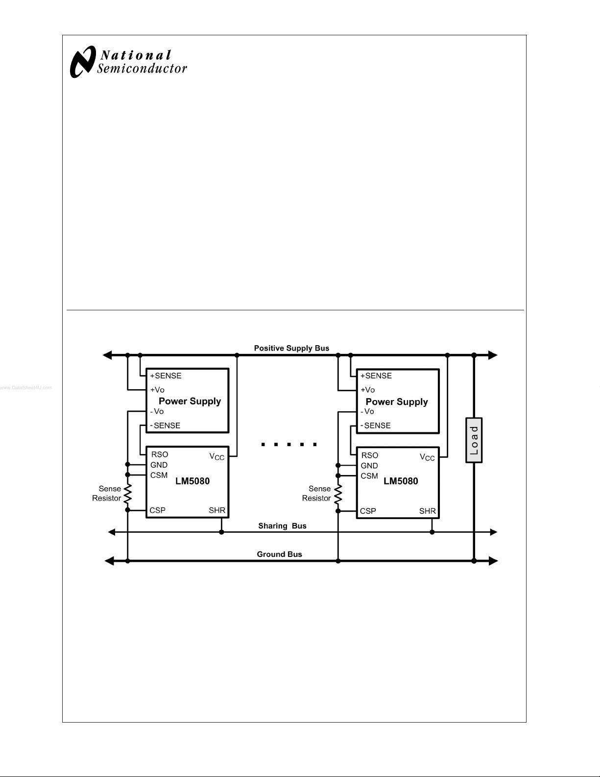
LM5080 Typical Application
Features
n Average program current share method
n Single-wire star link current share bus
n No precision external resistors necessary
n 3V to 15V bias voltage range
n Adaptable for high or low side current sensing
n Flexible architecture allows 4 modes of operation:
Negative remote sense adjustment
Positive remote sense adjustment
Trim or reference adjustment
Feedback divider adjustment
Packages
n MSOP-8
n RoHS compliant Pb free available
Remote Sense Adjust Mode
20157801
© 2006 National Semiconductor Corporation DS201578 www.national.com
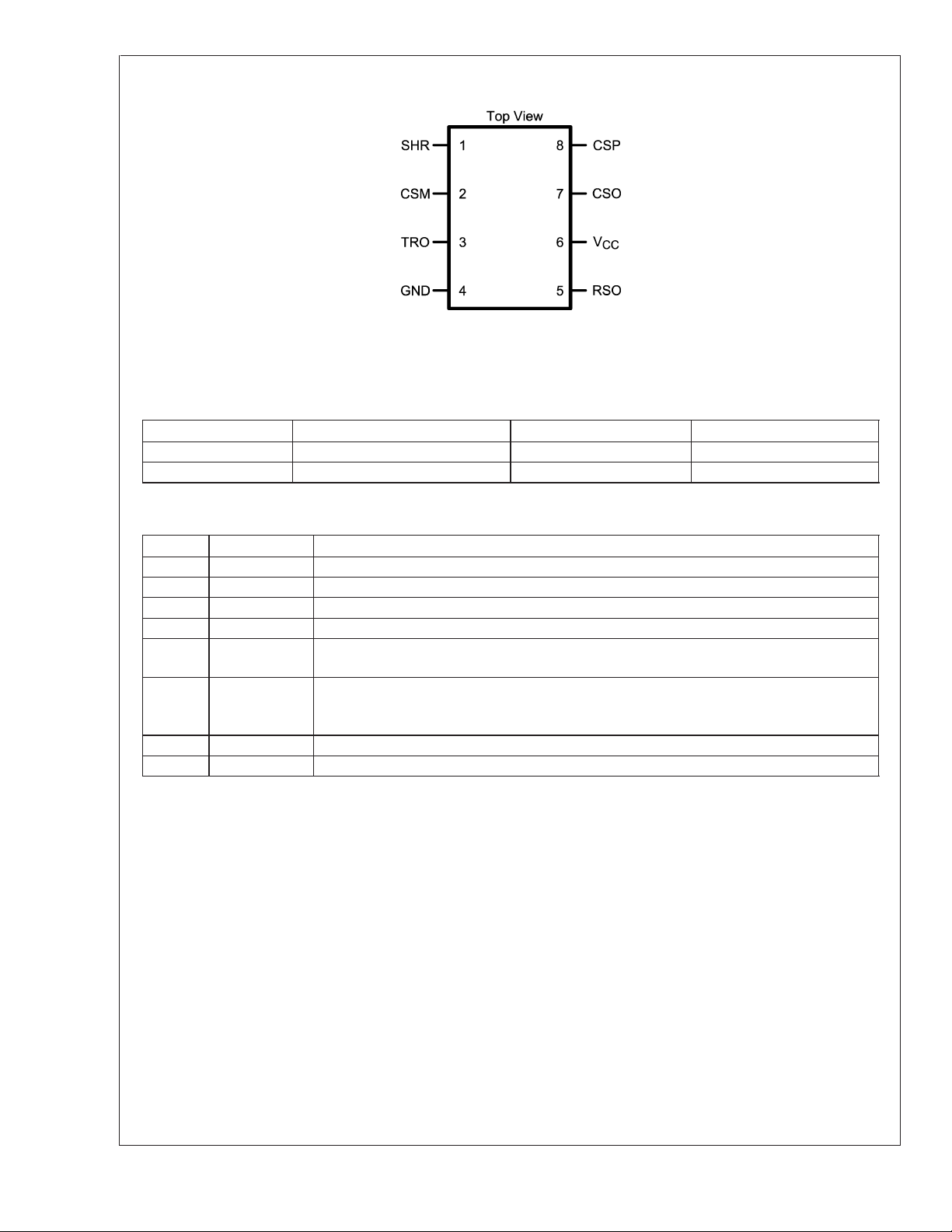
Connection Diagram
LM5080
8-Lead MSOP
See NS Package Number MUA08A
20157802
Ordering Information
Order Number Description NSC Package Drawing Supplied As
LM5080MM MSOP-8 MUA08A 1000 Units on Tape and Reel
LM5080MMX MSOP-8 MUA08A 3500 Units on Tape and Reel
Pin Descriptions
Pin Name Description
1 SHR Current Share Bus. The SHR pins of each LM5080 device are connected together.
2 CSM Current Sense Amplifier Minus Input.
3 TRO Transconductance Output. One of two outputs of the current sense transconductance amplifier.
4 GND Ground. Connect to negative terminal of the LM5080 bias supply.
5 RSO Remote Sense Output. Capable of driving the low impedance remote sense pin of a power
converter.
6 VCC Bias Supply. VCC can be connected to the output of the power converter that the LM5080
controls if greater than 3V, or it can be connected to another bias source for lower voltage
systems.
7 CSO Current Sense Output. One of two outputs of the current sense transconductance amplifier.
8 CSP Current Sense Amplifier Positive Input.
www.national.com 2
LM5080
Absolute Maximum Ratings (Note 1)
If Military/Aerospace specified devices are required,
Storage Temperature -55˚C to +150˚C
Junction Temperature 150˚C
please contact the National Semiconductor Sales Office/
Distributors for availability and specifications.
Operating Ratings (Note 1)
to GND -0.3V to 15V
V
CC
RSO to GND (Note 2) -0.3V to 5V
All other pins to GND -0.3V to 5V
ESD Rating (Note 3)
Human Body Model 2kV
Electrical Characteristics Limits in standard type are for T
the junction temperature range of –40˚C to +125˚C and are provided for reference only. Unless otherwise specified, the following conditions apply: CSM = 0, VCC = 5V, RSO unloaded.
Symbol Parameter Conditions Min Typ Max Units
ICC VCC Quiescent Current RSO shorted to CSO
CSP=50mV
CTRO = 10nF
CSP Input open circuit voltage ratio Specified as a percentage of VCC 19 20 21 %
CSP mode threshold ratio- Rising Specified as a percentage of VCC 8.5 10.5 12.5 %
CSP mode threshold ratio - Falling Specified as a percentage of VCC 7.0 9.5 11 %
Current Share Amplifier
VIO Input Offset Voltage (RSO-CSP) RSO shorted to CSO
CSP=50mV
CTRO = 10nF
RSO shorted to CSO
CSP = 600 mV
CTRO = 10nF, VCC = 3V
CSM
MAX
Input Common Mode Voltage
Range
CSM
MIN
GM
TRO
Current Share Amplifier
Transconductance
I
TRO_SRC
I
TRO_SINK
I
TRO_OS
V
TRO_MIN
V
TRO_MAX
TRO sourcing current limit TRO = 500 mV
TRO sinking current limit TRO = 500 mV
TRO offset current TRO = 750 mV
TRO Output Range CSP, CSO, SHA open circuit
RSO Buffer
VIO
I
LIMSRC
I
LIMSNK
VOL
RSO
RSO
RSO Buffer Input offset Voltage Offset = TRO-RSO, TR0 = 750 mV
RSO source current limit 18 26 35 mA
RSO sink current limit 18 26 35 mA
RSO output low voltage CSP = 0V, Sinking 10 mA 12 28 mV
Thermal Resistance
θ
JA
Junction to Ambient MSOP-8 Package 190 ˚C/W
CSP-CSM=50mV
RSO shorted to CSO
CSO-CSP
CTRO=10nF
GM
TRO
CTRO=10nF
CSO open, CSP = 1.1V
CSO open, CSP=0.9V
CSP, CSO Open Circuit
ITRO_OS
CSO, CSP open circuit
VCC to GND 3V to 14 V
Operating Junction Temperature -40˚C to +125˚C
= 25˚C only; limits in boldface type apply over
J
3.7 5.5 mA
-2.5
0 2.5
-3.5
-1
012mV
-2
VCC-2V V
<
1mV
= ∆ITRO / ∆VSHR
0V
8.7 mA/V
9 11 14 µA
8.2 11 13.5 µA
–1 0 1 µA
450 mV
<
500 nA
2.75 V
-4 0 4 mV
3.5
mV
www.national.com3
Electrical Characteristics Limits in standard type are for T
the junction temperature range of –40˚C to +125˚C and are provided for reference only. Unless otherwise specified, the
LM5080
following conditions apply: CSM = 0, VCC = 5V, RSO unloaded. (Continued)
Note 1: Absolute Maximum Ratings are limits beyond which damage to the device may occur. Operating Ratings indicate conditions for which the device is intended
to be functional, but does not guarantee specific perfromance limits. For guaranteed specifications and test conditions see the Electrical Characteristics.
Note 2: Maximum recommended operating voltage not to exceed VCC - 2V or 5V, whichever is lower.
Note 3: The human body model is a 100 pF capacitor discharged through a 1.5 kΩ resistor into each pin.
= 25˚C only; limits in boldface type apply over
J
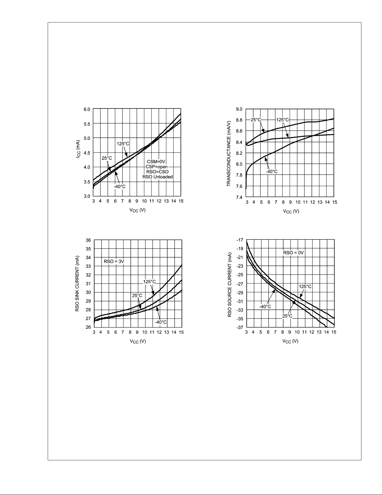
Typical Performance Characteristics
ICCvs V
CC
20157817
Current Share Amplifier Transconductance vs VCC
RSO Sink Current Limit vs VCC RSO Source Current Limit vs VCC
20157818
20157819
www.national.com 4
20157820
 Loading...