

LITTELFUSE V9MLA0805LWT, V9MLA0805LWA, V9MLA0805LWH, V9MLA0805LT, V9MLA0805LH Datasheet
...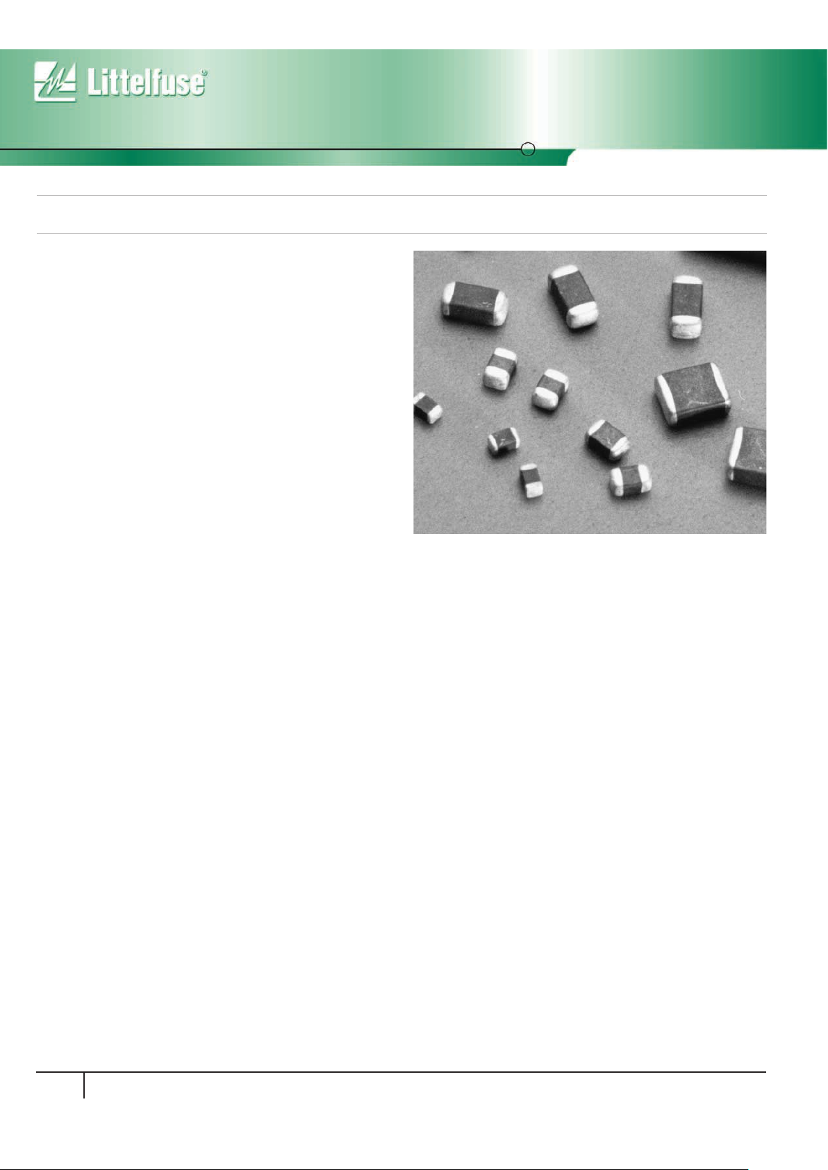
Multilayer Transient Voltage Surge Suppressors
ML Varistor Series
Surface Mount Varistors
140
www.littelfuse.com
The ML Series family of Transient Voltage Surge Suppression devices is
based on the Littelfuse Multilayer fabrication technology. These components are designed to suppress a variety of transient events, including
those specified in IEC 61000-4-2 or other standards used for Electromagnetic
Compliance (EMC). The ML Series is typically applied to protect integrated
circuits and other components at the circuit board level.
The wide operating voltage and energy range make the ML Series suitable for numerous applications on power supply, control and signal lines.
The ML Series is manufactured from semiconducting ceramics, and is
supplied in a leadless, surface mount package.The ML Series is compatible with modern reflow and wave soldering procedures.
It can operate over a wider temperature range than zener diodes, and
has a much smaller footprint than plastic-housed components.
Littelfuse Inc. manufactures other Multilayer Series products. See the
MLE Series data sheet for ESD applications, MHS Series data sheet for
high-speed ESD applications, the MLN for multiline protection and the
AUML Series for automotive applications.
Features
• Leadless 0402, 0603, 0805, 1206 and 1210 Chip Sizes
• Multilayer Ceramic Construction Technology
•-55oC to +125oC Operating Temperature Range
• Operating Voltage Range V
M(DC)
= 5.5V to 120V
• Rated for Surge Current (8 x 20µs)
• Rated for Energy (10 x 1000µs)
• Inherent Bi-directional Clamping
• No Plastic or Epoxy Packaging Assures Better than 94V-0
Flammability Rating
• Standard Low Capacitance Types Available
Applications
• Suppression of Inductive Switching or Other Transient Events Such
as EFT and Surge Voltage at the Circuit Board Level
• ESD Protection for Components Sensitive to IEC 61000-4-2,
MIL-STD-883C Method 3015.7, and Other Industry Specifications
(See Also the MLE or MLN Series)
• Provides On-Board Transient Voltage Protection for ICs and Transistors
• Used to Help Achieve Electromagnetic Compliance of End Products
• Replace Larger Surface Mount TVS Zeners in
Many Applications
Absolute Maximum Ratings For ratings of individual members of a series, see Device Ratings and Specifications table.
Continuous:
Steady State Applied Voltage:
DC Voltage Range (V
M(DC)
). . . . . . . . . . . . . . . . . . . . . . . . . . . . . . . . . . . . . . . . . . . . . . . . . . . . . . . . . . . . . . . . . . . . . . . . . 3.5 to 120 V
AC Voltage Range (V
M(AC)RMS
) . . . . . . . . . . . . . . . . . . . . . . . . . . . . . . . . . . . . . . . . . . . . . . . . . . . . . . . . . . . . . . . . . . . . . 2.5 to 107 V
Transient:
Non-Repetitive Surge Current, 8/20µs Waveform, (ITM) . . . . . . . . . . . . . . . . . . . . . . . . . . . . . . . . . . . . . . . . . . . . . . . . . . . . . 4 to 500 A
Non-Repetitive Surge Energy, 10/1000µs Waveform, (WTM) . . . . . . . . . . . . . . . . . . . . . . . . . . . . . . . . . . . . . . . . . . . . . . . . . 0.2 to 2.5 J
Operating Ambient Temperature Range (TA) . . . . . . . . . . . . . . . . . . . . . . . . . . . . . . . . . . . . . . . . . . . . . . . . . . . . . . . . . . . . . . -55 to + 125
O
C
Storage Temperature Range (T
STG
) . . . . . . . . . . . . . . . . . . . . . . . . . . . . . . . . . . . . . . . . . . . . . . . . . . . . . . . . . . . . . . . . . . . . -55 to + 150
O
C
Temperature Coefficient (αV) of Clamping Voltage (VC) at Specified Test Current . . . . . . . . . . . . . . . . . . . . . . . . . . . . . . . . . . . . . <0.01 %/OC
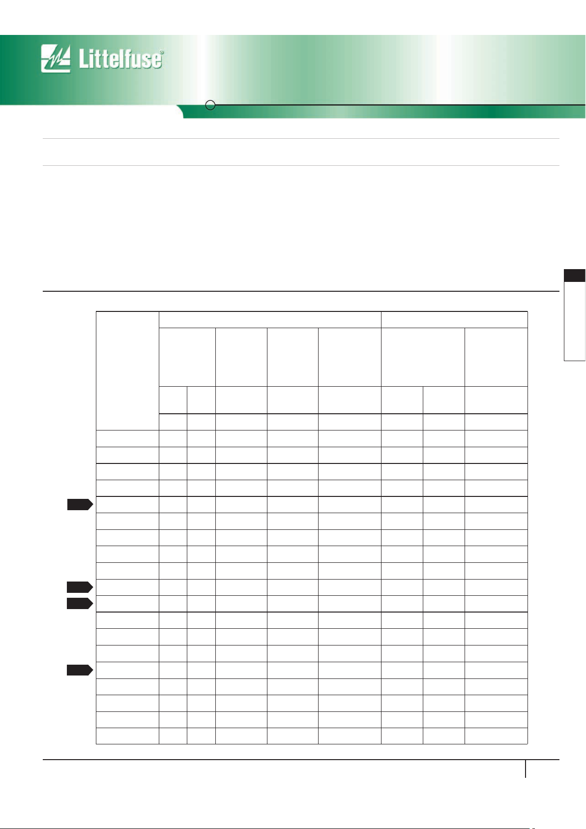
Device Ratings and Specifications
ML SERIES UNITS
PA RT
NUMBER
MAXIMUM RATINGS (125
o
C) SPECIFICATIONS (25oC)
MAXIMUM
CONTINUOUS
WORKING
VO LTAGE
MAXIMUM
NON-
REPETITIVE
SURGE
CURRENT
(8/20µs)
MAXIMUM
NON-
REPETITIVE
SURGE
ENERGY
(10/1000µs)
MAXIMUM
CLAMPING
VO LTAG E AT
10A
(OR AS NOTED)
(8/20µs)
NOMINAL VOLTAGE
AT 1mA DC TEST
CURRENT
TYPICAL
CAPACITANCE
AT f = 1MHz
V
M(DC)VM(AC)
I
TM
W
TM
V
C
V
N(DC)
MIN
V
N(DC)
MAX C
(V) (V) (A) (J) (V) (V) (V) (pF)
V3.5MLA0603 3.5 2.5 30 0.1 10 at 2A 3.7 7.0 1100
V3.5MLA0805 3.5 2.5 120 0.3 10 at 5A 3.7 7.0 2200
V3.5MLA0805L 3.5 2.5 40 0.1 10 at 2A 3.7 7.0 1200
V3.5MLA1206 3.5 2.5 100 0.3 14 3.7 7.0 6000
V5.5MLA0402 5.5 4.0 20 0.050 15.5 at 1A 7.1 9.3 220
V9MLA0402 9 6.5 20 0.050 22 at 1A 11 14 120
V9MLA0402L 9 6.5 4 0.020 25 at 1A 11 14 33
V14MLA0402 14 10 20 0.050 30 at 1A 15.9 20.3 70
V5.5MLA0603 5.5 4.0 30 0.1 15.5 at 2A 7.1 9.3 660
V5.5MLA0805 5.5 4.0 120 0.3 15.5 at 5A 7.1 9.3 1600
V5.5MLA0805L 5.5 4.0 40 0.1 15.5 at 2A 7.1 9.3 860
V5.5MLA1206 5.5 4.0 150 0.4 15.5 7.1 9.3 4500
V9MLA0603 9.0 6.5 30 0.1 23 at 2A 11.0 16.0 420
V9MLA0805L 9.0 6.5 40 0.1 20 at 2A 11 14 450
V12MLA0805L 12 9.0 40 0.1 25 at 2A 14 18.5 350
V14MLA0603 14 10 30 0.1 30 at 2A 15.9 20.3 150
V14MLA0805 14 10 120 0.3 30 at 5A 15.9 20.3 480
V14MLA0805L 14 10 40 0.1 30 at 2A 15.9 20.3 270
V14MLA1206 14 10 150 0.4 30 15.9 20.3 1600
NEW
NEW
NEW
NEW
ML Varistor Series
Surface Mount Varistors
Multilayer Transient Voltage Surge Suppressors
141
www.littelfuse.com
3
SURFACE MOUNT
VARISTORS
Multilayer Transient Voltage Surge Suppressors
ML Varistor Series
Surface Mount Varistors
142
www.littelfuse.com
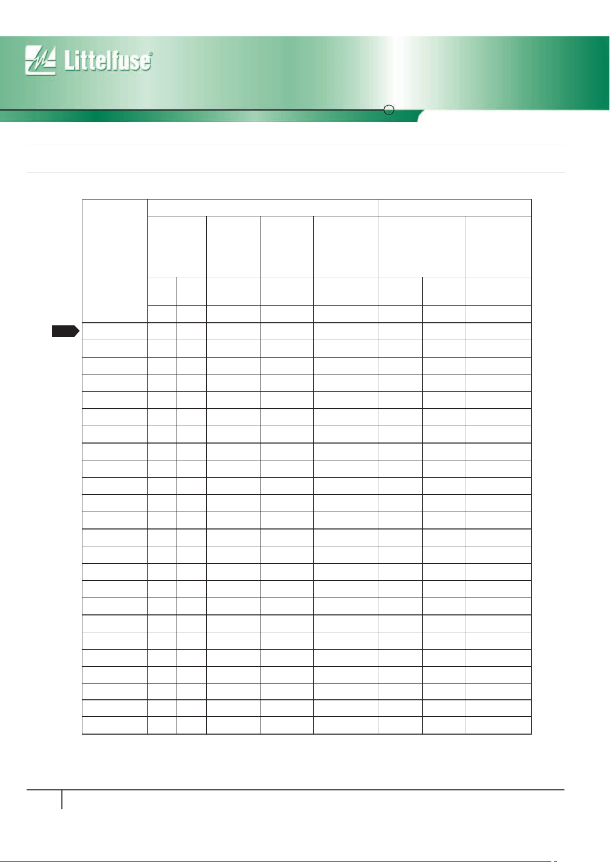
Device Ratings and Specifications
(Continued)
V18MLA0603 18 14 30 0.1 40 at 2A 22 28.0 125
V18MLA0402 18 14 20 0.050 40 at 1A 22 28.0 40
V18MLA0805 18 14 120 0.3 40 at 5A 22 28.0 450
V18MLA0805L 18 14 40 0.1 40 at 2A 22 28.0 250
V18MLA1206 18 14 150 0.4 40 22 28.0 1100
V18MLA1210 18 14 500 2.5 40 22 28.0 1250
V26MLA0603 26 20 30 0.1 58 at 2A 31 38 90
V26MLA0805 26 20 100 0.3 58 at 5A 29.5 38.5 190
V26MLA0805L 26 20 40 0.1 58 at 2A 29.5 38.5 115
V26MLA1206 26 20 150 0.6 56 29.5 38.5 900
V26MLA1210 26 20 300 1.2 54 29.5 38.5 1000
V30MLA0603 30 25 30 0.1 65 at 2A 37 46 75
V30MLA0805L 30 25 30 0.1 65 at 2A 37 46 80
V30MLA1210 30 25 280 1.2 62 35 43 1575
V30MLA1210L 30 25 220 0.9 62 35 43 1530
V33MLA1206 33 26 180 0.8 72 38 49 550
V42MLA1206 42 30 180 0.8 86 46 60 550
V48MLA1210 48 40 250 1.2 100 54.5 66.5 450
V48MLA1210L 48 40 220 0.9 100 54.5 66.5 430
V56MLA1206 56 40 180 1.0 110 61 77 150
V60MLA1210 60 50 250 1.5 120 67 83 375
V68MLA1206 68 50 180 1.0 130 76 90 150
V85MLA1210 85 67 250 2.5 160 95 115 225
V120MLA1210 120 107 125 2.0 230 135 165 65
NOTES:
1.
2.
3.
PA RT
NUMBER
MAXIMUM RATINGS (125
o
C) SPECIFICATIONS (25oC)
MAXIMUM
CONTINUOUS
WORKING
VO LTAGE
MAXIMUM
NON-
REPETITIVE
SURGE
CURRENT
(8/20µs)
MAXIMUM
NON-
REPETITIVE
SURGE
ENERGY
(10/1000µs)
MAXIMUM
CLAMPING
VO LTAG E AT
10A
(OR AS NOTED)
(8/20µs)
NOMINAL VOLTAGE
AT 1mA DC TEST
CURRENT
TYPICAL
CAPACITANCE
AT f = 1MHz
V
M(DC)VM(AC)
I
TM
W
TM
V
C
V
N(DC)
MIN
V
N(DC)
MAX C
(V) (V) (A) (J) (V) (V) (V) (pF)
L suffix is a low capacitance and energy version; Contact your Littelfuse Sales Representative for custom capacitance requirements.
Typical leakage at 25 C<25µA, maximum leakage 50µA at V ; for 0402 size, typical leakage <5µA, maximum leakage 10µA at V
o
M(DC)
M(DC).
Average power dissipation of transients for 0402, 0603, 0805, 1206 and 1210 sizes not to exceed 0.03W, 0.05W, 0.1W, 0.1W and 0.15W respectively.
NEW
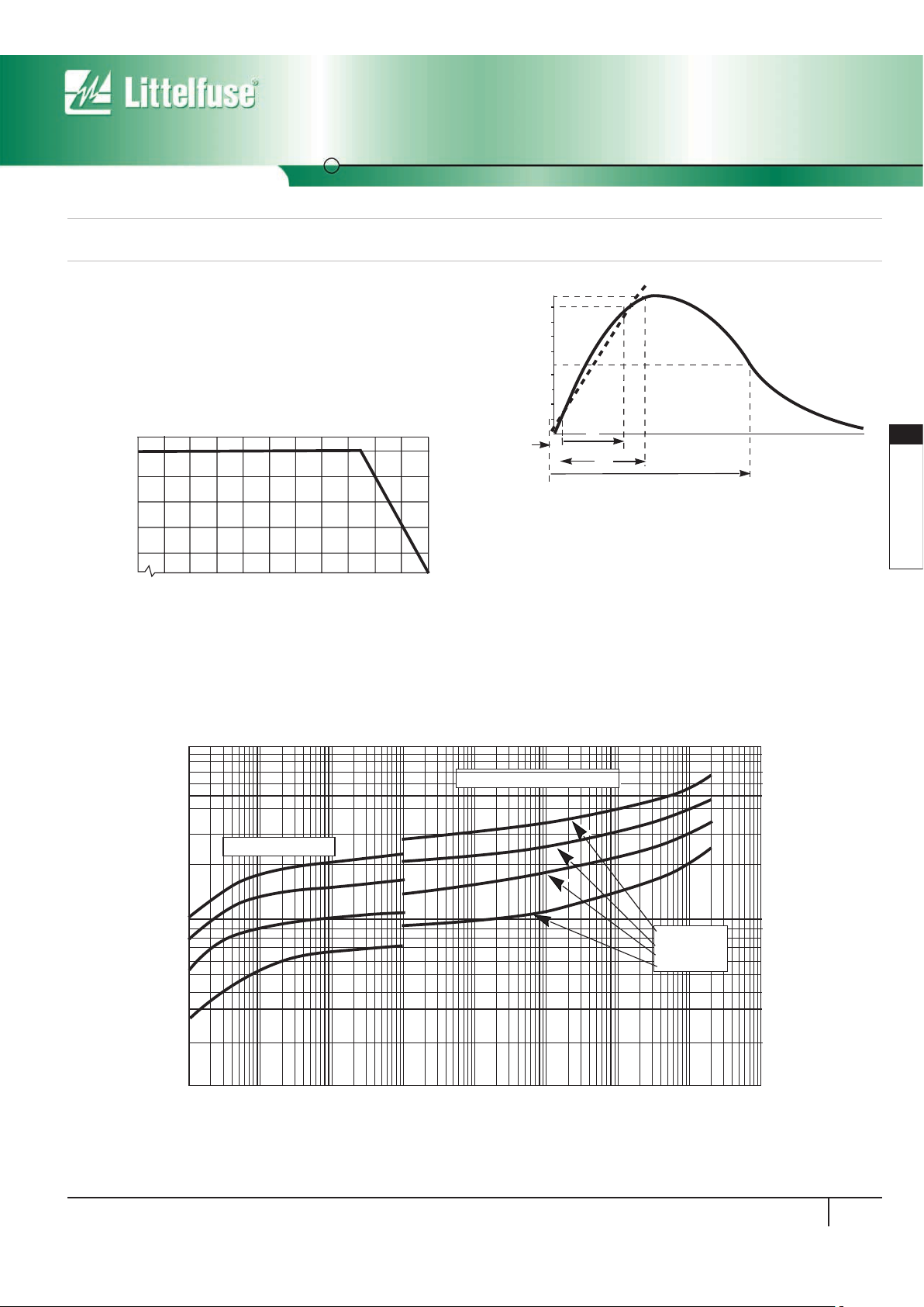
Temperature De-rating
When transients occur in rapid succession, the average power dissipation is the energy (watt-seconds) per pulse times the number of pulses
per second. The power so developed must be within the specifications
shown on the Device Ratings and Specifications table for the specific
device. For applications exceeding 125oC ambient temperature, the peak
surge current and energy ratings must be derated as shown in Figure 1.
100
80
60
40
20
0
-55 50 60 70 80 90 100 110 120 130 140 150
PERCENT OF RATED VALUE
AMBIENT TEMPERATURE (oC)
FIGURE 1. PEAK CURRENT AND ENERGY
DERATING CURVE
t
1
t
2
100
50
0
O
1
TIME
PERCENT OF PEAK VALUE
O1 = VIRTUAL ORIGIN OF WAVE
t
1
= VIRTUAL FRONT TIME = 1.25 x t
(IMPULSE DURATION)
t = TIME FROM 10% TO 90% OF PEAK
t
2
= VIRTUAL TIME TO HALF VALUE
EXAMPLE:
FOR AN 8/20µs CURRENT WAVEFORM
8µs = t
1
= VIRTUAL FRONT TIME
20µs = t
2
= VIRTUAL TIME TO
HALF VALUE
FIGURE 2. PEAK PULSE CURRENT TEST WAVEFORM
FOR CLAMPING VOLTAGE
t
FIGURE 3. LIMIT V-I CHARACTERISTIC FOR V5.5MLA0402 TO V18MLA0402
100
10
1µA
CURRENT (A)
Varistor Voltage (V)
MAXIMUM LEAKAGE
10µA 100 µA 1mA 10mA 100mA 1A 10A 100A
MAXIMUM CLAMPING VOLTAGE
V18MLA0402
V14MLA0402
V09MLA0402
V5.5MLA0402
ML Varistor Series
Surface Mount Varistors
Multilayer Transient Voltage Surge Suppressors
143
www.littelfuse.com
3
SURFACE MOUNT
VARISTORS

Multilayer Transient Voltage Surge Suppressors
ML Varistor Series
Surface Mount Varistors
144
www.littelfuse.com
Maximum Transient V-I Characteristic Curves
FIGURE 5. LIMIT V-I CHARACTERISTIC FOR V3.5MLA0603 TO V30MLA0603
100
10
1µA
CURRENT (A)
Varistor Voltage (V)
V3.5MLA0603
MAXIMUM LEAKAGE
MAXIMUM CLAMPING VOLTAGE
V5.5MLA0603
V9MLA0603
10µA 100µA 1mA 10mA 100mA 1A 10A 100A
V14MLA0603
V18MLA0603
V26MLA0603
V30MLA0603
FIGURE 6. LIMIT V-I CHARACTERISTIC FOR V3.5MLA0805L TO V30MLA0805L
100
10
1µA
CURRENT (A)
Varistor Voltage (V)
V3.5MLA0805L
MAXIMUM LEAKAGE
MAXIMUM CLAMPING VOLTAGE
V5.5MLA
0805L
V9MLA0805L
10µA 100µA 1mA 10mA 100mA 1A 10A 100A
V14MLA0805L
V18MLA0805L
V26MLA0805L
V30MLA0805L
FIGURE 4. LIMIT V-I CHARACTERISTIC FOR V9MLA0402L
100
10
1µA
CURRENT (A)
Varistor Voltage (V)
10µA 100µ A 1mA 10mA 100mA 1A 10A
MAXIMUM LEAKAGE
MAXIMUM CLAMPING VOLTAGE
V9MLA0402L

Maximum Transient V-I Characteristic Curves (Continued)
FIGURE 7. LIMIT V-I CHARACTERISTIC FOR V3.5MLA0805 TO V26MLA0805
1mA
100
10
1µA
CURRENT (A)
Varistor Voltage (V)
10µA 100µA 10mA 100mA 1A 10A 100A 1000A
V3.5MLA0805
MAXIMUM CLAMPING VOLTAGE
MAXIMUM LEAKAGE
V14MLA0805
V5.5MLA0805
V18MLA0805
V26MLA0805
FIGURE 9. LIMIT V-I CHARACTERISTIC FOR V18MLA1210 TO V120MLA1210
1mA
100
10
1µA
CURRENT (A)
Varistor Voltage (V)
10µA 100µA 10mA 100mA 1A 10A 100A 1000A
MAXIMUM CLAMPING VOLTAGE
MAXIMUM LEAKAGE
1000
1
V60MLA1210
V85MLA1210
V120MLA1210
V48MLA1210, V48MLA1210L
V30MLA1210, V30MLA1210L
V26MLA1210
V18MLA1210
FIGURE 8. LIMIT V-I CHARACTERISTIC FOR V3.5MLA1206 TO V68MLA1206
1mA1µA
CURRENT (A)
Varistor Voltage (V)
10mA 1000A100mA 1A 10A 100A
MAXIMUM CLAMP
VOLTAG E
10µA 100µA
MAXIMUM
LEAKAGE
V56MLA1206
V42MLA1206
V26MLA1206
V33MLA1206
V18MLA1206
V68MLA1206
V3.5MLA1206
V5.5MLA1206
V14MLA1206
100
10
1
1000
ML Varistor Series
Surface Mount Varistors
Multilayer Transient Voltage Surge Suppressors
145
www.littelfuse.com
3
SURFACE MOUNT
VARISTORS

Multilayer Transient Voltage Surge Suppressors
ML Varistor Series
Surface Mount Varistors
146
www.littelfuse.com
Device Characteristics
At low current levels, the V-I curve of the multilayer transient voltage
suppressor approaches a linear (ohmic) relationship and shows a
temperature dependent effect (Figure 10). At or below the maximum
working voltage, the suppressor is in a high resistance mode (approaching 106Ω at its maximum rated working voltage). Leakage currents at
maximum rated voltage are below 50µA, typically 25µA; for 0402 size
below 10µA, typically 5µA.
Speed of Response
The Multilayer Suppressor is a leadless device. Its response time is not
limited by the parasitic lead inductances found in other surface mount
packages. The response time of the Zinc Oxide dielectric material is less
than 1 nanosecond and the ML can clamp very fast dV/dT events such
as ESD. Additionally, in “real world” applications, the associated circuit
wiring is often the greatest factor effecting speed of response. Therefore,
transient suppressor placement within a circuit can be considered
important in certain instances.
100%
1E
-9
1E
-8
SUPPRESSOR CURRENT (ADC)
10%
1E
-7
1E
-6
1E
-5
1E
-4
1E
-3
1E
-2
25 50 75 100
125oC
SUPPRESSOR VOLTAGE IN PERCENT OF
V
NOM
VALUE AT 25
o
C (%)
FIGURE 10. TYPICAL TEMPERATURE DEPENDANCE OF THE CHARACTERISTIC
CURVE IN THE LEAKAGE REGION
o
oo
o
GRAINS
DEPLETION
FIRED CERAMIC
DIELECTRIC
REGION
METAL
ELECTRODES
DEPLETION
REGION
METAL END
TERMINATION
FIGURE 11. MULTILAYER INTERNAL CONSTRUCTION
Energy Absorption/Peak Current Capability
Energy dissipated within the ML is calculated by multiplying the clamping
voltage, transient current and transient duration. An important advantage
of the multilayer is its interdigitated electrode construction within the mass
of dielectric material. This results in excellent current distribution and the
peak temperature per energy absorbed is very low.The matrix of semiconducting grains combine to absorb and distribute transient energy (heat)
(Figure 11). This dramatically reduces peak temperature; thermal stresses
and enhances device reliability.
As a measure of the device capability in energy and peak current
handling, the V26MLA1206A part was tested with multiple pulses at its
peak current rating (150A, 8/20µs). At the end of the test, 10,000 pulses
later, the device voltage characteristics are still well within specification
(Figure 13).
100
10
20
V26MLA1206
40 60 80 100 120 140
TEMPERATURE (
o
C)
CLAMPING VO LTAGE (V)
V5.5MLA1206
0-20-40-60
FIGURE 12. CLAMPING VOLTAGE OVER TEMPERATURE
(V
C
AT 10A)
100
10
0
V26MLA1206
2000 4000 6000 8000 10000 12000
NUMBER OF PULSES
VO LTAGE
FIGURE 13. REPETITIVE PULSE CAPABILITY
PEAK CURRENT = 150A
8/20µs DURATION, 30s BETWEEN PULSES

Soldering Recommendations
The principal techniques used for the soldering of components in surface
mount technology are Infrared (IR) re-flow, vapour phase re-flow and wave
soldering. Typical profiles are shown in Figures 14, 15 and 16. When wave
soldering, the ML suppressor is attached to the circuit board by means of an
adhesive. The assembly is then placed on a conveyor and run through the
soldering process to contact the wave. With IR and vapour phase reflow; the
device is placed in a solder paste on the substrate. As the solder paste is
heated, it re-flows and solders the unit to the board.
The recommended solder for the ML suppressor is a 62/36/2 (Sn/Pb/Ag),
60/40 (Sn/Pb) or 63/37 (Sn/Pb). Littelfuse also recommends an RMA
solder flux.
Wave soldering is the most strenuous of the processes. To avoid the
possibility of generating stresses due to thermal shock, a preheat stage
in the soldering process is recommended, and the peak temperature of
the solder process should be rigidly controlled. For 0402 size devices, IR
re-flow is recommended.
When using a reflow process, care should be taken to ensure that the ML
chip is not subjected to a thermal gradient steeper than 4 degrees per
second; the ideal gradient being 2 degrees per second. During the
soldering process, preheating to within 100 degrees of the solder’s peak
temperature is essential to minimize thermal shock. Examples of the
soldering conditions for the ML suppressor are given in the tables below.
Once the soldering process has been completed, it is still necessary
to ensure that any further thermal shocks are avoided. One possible
cause of thermal shock is hot printed circuit boards being removed
from the solder process and subjected to cleaning solvents at room
temperature. The boards must be allowed to cool gradually to less than
50oC before cleaning.
Termination Options
Littelfuse offers three types of electrode termination finish for the
Multilayer product series:
1. Silver/Platinum (standard, not available for 0402)
2. Silver/Palladium (optional)
(The ordering information section describes how to designate them.)
FIGURE 14. REFLOW SOLDER PROFILE
FIGURE 15. WAVE SOLDER PROFILE
FIGURE 16. VAPOR PHASE SOLDER PROFILE
TEMPERATURE (
o
C)
TIME (MINUTES)
300
250
200
150
100
50
0
0.0 0.5 1.0 1.5 2.0 2.5 3.0 3.5 4.0 4.5
MAXIMUM WAVE 260oC
SECOND PREHEAT
FIRST PREHEAT
TEMPERATURE (
o
C)
TIME (MINUTES)
250
200
150
100
50
0
0.0 0.5 1.0 1.5 2.0 2.5 3.0 3.5
RAMP RATE
PREHEAT ZONE
>50
o
C/s
MAXIMUM
TEMPERATURE 222
o
C
40-80
SECONDS
ABOVE 183
o
C
TEMPERATURE (
o
C)
TIME (MINUTES)
250
200
150
100
50
0
0.0 0.5 1.0 1.5 2.0 2.5 3.0 3.5 4.0
MAXIMUM
PREHEAT DWELL
PREHEAT ZONE
TEMPERATURE 222
o
C
RAMP RATE
<2
o
C/s
40-80
SECONDS
ABOVE 183
o
C
ML Varistor Series
Surface Mount Varistors
Multilayer Transient Voltage Surge Suppressors
147
www.littelfuse.com
3
SURFACE MOUNT
VARISTORS
3. Nickel Barrier (optional for 0402-1210 package size)
(The ordering information section describes how to designate them.)

Multilayer Transient Voltage Surge Suppressors
ML Varistor Series
Surface Mount Varistors
148
www.littelfuse.com
Recommended Pad Outline
C
B
A
NOTE: Avoid metal runs in this area.
NOTE
DIMENSION
PAD SIZE
1210
SIZE DEVICE
1206
SIZE DEVICE
0805
SIZE DEVICE
0603
SIZE DEVICE
IN MM IN MM IN MM IN MM
A 0.160 4.06 0.160 4.06 0.120 3.05 0.100 2.54
B 0.100 2.54 0.065 1.65 0.050 1.27 0.030 0.76
C 0.040 1.02 0.040 1.02 0.040 1.02 0.035 0.89
TABLE 1: PAD LAYOUT DIMENSIONS
0402
SIZE DEVICE
IN MM
0.067 1.70
0.020 0.51
0.024 0.61

Ordering Information
VXXML TYPES
E
L
W
D
Mechanical Dimensions
V 18 1206
PACKING OPTIONS
T: 13in (330mm) Diameter Reel
H: 7in (178mm) Diameter Reel (Note)
A: Bulk Pack
DEVICE SIZE:
i.e 120 mil x 60 mil
DEVICE FAMILY
Littelfuse TVSS Device
X
MAXIMUM DC
WORKING VOLTAGE
MLA X X
CAPACITANCE OPTION
No Letter:Standard
L: Low Capacitance Version
END TERMINATION OPTION
No Letter: Ag/Pt (Standard)
W: Ag/Pd
MULTILAYER SERIES
DESIGNATOR
(3MM X 1.5MM)
N: Nickel Barrier (0402 -1210). For 0402 package size,
Nickel Barrier termination is subject to availibility.
Please contact a Littelfuse sales representative.
DIMENSION
CHIP SIZE
1210 1206 0805 0603
IN MM IN MM IN MM IN MM
D Max. 0.113 2.87 0.071 1.80 0.043 1.10 0.035 0.90
E 0.02 ±0.01 0.50 ±0.25 0.02 ±0.01 0.50 ±0.25 0.01 to 0.029 0.50 to 0.25 0.015 ±0.008 0.4 ±0.2
L 0.125 ±0.012 3.20 ±0.30 0.125 ±0.012 3.20 ±0.30 0.079 ±0.008 2.01 ±0.20 0.063 ±0.006 1.6 ±0.15
W 0.10 ±0.012 2.54 ±0.30 0.06 ±0.011 1.60 ±0.28 0.049 ±0.008 1.25 ±0.20 0.032 ±0.06 0.8 ±0.15
0402
IN MM
0.024 0.61
0.010 ±0.006 0.25 ±0.15
0.039 ±0.004 1.0 ±0.1
0.020 ±0.004 0.5 ±0.1
Standard Shipping Quantities
DEVICE SIZE “13” INCH REEL (“T” OPTION) “7” INCH REEL (“H” OPTION) BULK PACK (“A” OPTION)
1210 8,000 2,500 2500
1206 10,000 2,500 2500
0805 10,000 2,500 2500
0603 10,000 2,500 2500
0402 N/A 10,000 N/A
ML Varistor Series
Surface Mount Varistors
Multilayer Transient Voltage Surge Suppressors
149
www.littelfuse.com
3
SURFACE MOUNT
VARISTORS

Multilayer Transient Voltage Surge Suppressors
ML Varistor Series
Surface Mount Varistors
150
www.littelfuse.com
Tape and Reel Specifications
• Conforms to EIA - 481-1, Revision A
• Can be supplied to IEC Publication 286 - 3
SYMBOL DESCRIPTION
DIMENSIONS IN MILLIMETERS
A
0
Width of Cavity Dependent on Chip Size to Minimize Rotation.
B
0
Length of Cavity Dependent on Chip Size to Minimize Rotation.
K
0
Depth of Cavity Dependent on Chip Size to Minimize Rotation.
W Width of Tape 8 ±0.2
F Distance Between Drive Hole Centers and Cavity Centers 3.5 ±0.05
E Distance Between Drive Hole Centers and Tape Edge 1.75 ±0.1
P
1
Distance Between Cavity Centers 4 ±0.1
P
2
Axial Drive Distance Between Drive Hole Centers & Cavity Centers 2 ±0.1
P
0
Axial Drive Distance Between Drive Hole Centers 4 ±0.1
D
0
Drive Hole Diameter 1.55 ±0.05
D
1
Diameter of Cavity Piercing 1.05 ±0.05
T
1
0.1 Max
Top Tape Thickness
0402 Size 0603, 0805, 1206 & 1210 Sizes
2±0.05
N/A
K
0
t
1
D
0
P
0
D
1
P
1
A
0
P
2
B
0
F
E
W
PLASTIC CARRIER TAPE
EMBOSSMENT
TOP TAPE
8mm
NOMINAL
PRODUCT
IDENTIFYING
LABEL
178mm
OR 330mm
DIA. REEL
EMBOSSED PAPER (0402 SIZE ONLY)
 Loading...