

LITTELFUSE V18MLE1206H, V18MLE1206A, V18MLE0805WT, V18MLE0805WH, V18MLE0805WA Datasheet
...
3
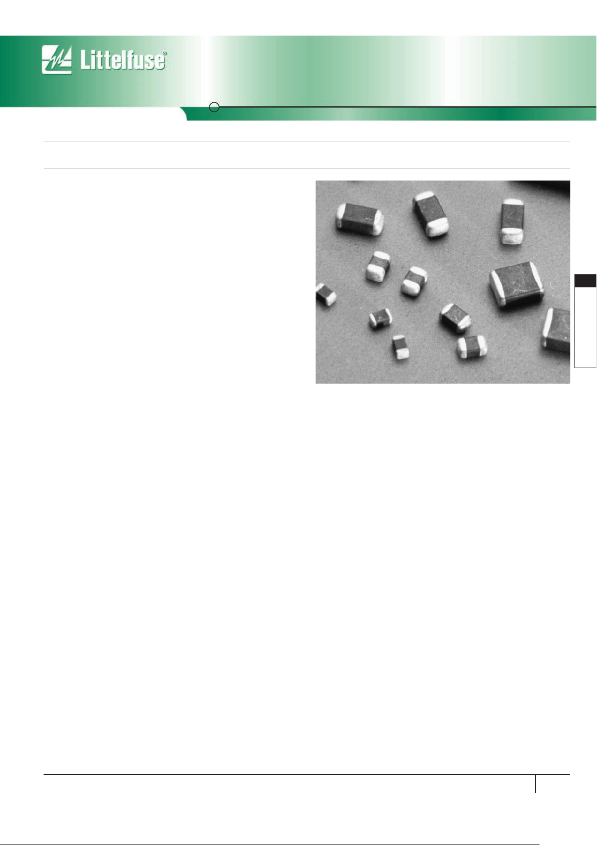
SURFACE MOUNT
VARISTORS
Surface Mount Varistors
133
www.littelfuse.com
Multilayer Transient Voltage Suppressor
MLE Varistor Series
The MLE Series family of Transient Voltage Suppression devices are based
on the Littelfuse Multilayer fabrication technology. These components are
designed to suppress ESD events, including those specified in IEC 610004-2 or other standards used for Electromagnetic Compliance testing. The
MLE Series is typically applied to protect integrated circuits and other
components at the circuit board level operating at 18VDC, or less.
The fabrication method and materials of these devices result in capacitance characteristics suitable for high frequency attenuation/low-pass
filter circuit functions, thereby providing suppression and filtering in a
single device.
The MLE Series is manufactured from semiconducting ceramics and is supplied in a leadless, surface mount package.The MLE Series is compatible
with modern reflow and wave soldering procedures.
Littelfuse Inc. manufactures other Multilayer Series products. See the ML
Series data sheet for higher energy/peak current transient applications. See
the AUML Series for automotive applications and the MLN Quad Array. For
high speed applications see the MHS series.
Features
• Rated for ESD (IEC-61000-4-2)
• Characterized for Impedance and Capacitance
•-55
o
C to +125oC Operating Temperature Range
• Leadless 0402, 0603, 0805, and 1206 sizes
• Operating Voltages up to 18V
M(DC)
• Multilayer Ceramic Construction Technology
Applications
• Protection of Components and Circuits Sensitive to ESD Transients
Occurring on Power Supplies, Control and Signal Lines
• Suppression of ESD Events Such as Specified in IEC-61000-4-2 or
MIL-STD-883C Method-3015.7, for Electromagnetic Compliance (EMC)
• Used in Mobile Communications, Computer/EDP Products, Medical
Products, Hand Held/Portable Devices, Industrial Equipment,
Including Diagnostic Port Protection and I/O Interfaces

Multilayer Transient Voltage Suppressor
MLE Varistor Series
Surface Mount Varistors
134
www.littelfuse.com
Absolute Maximum Ratings
For ratings of individual members of a series, see device ratings and specifications table.
Continuous:
Steady State Applied Voltage:
DC Voltage Range (V
M(DC)
) . . . . . . . . . . . . . . . . . . . . . . . . . . . . . . . . . . . . . . . . . . . . . . . . . . . . . . . . . . . . . . . . . . . . . . . . . . ≤18 V
Operating Ambient Temperature Range (TA) . . . . . . . . . . . . . . . . . . . . . . . . . . . . . . . . . . . . . . . . . . . . . . . . . . . . . . . . . . . . . . -55 to + 125
O
C
Storage Temperature Range (T
STG
). . . . . . . . . . . . . . . . . . . . . . . . . . . . . . . . . . . . . . . . . . . . . . . . . . . . . . . . . . . . . . . . . . . . -55 to + 150
O
C
Device Ratings and Specifications
PA RT
NUMBER
MAX CONTINUOUS
WORKING VOLTAGE
-55
o
C TO 125oC
PERFORMANCE SPECIFICATIONS (25
o
C)
NOMINAL
VO LTAGE
TYPICAL
CAPACITANCE
AT 1MHz
MAXIMUM
LEAKAGE
(NOTE 1)
V
M(DC)
V
NOM
AT
1mA DC I
L MAX
AT APPLIED
VO LTAGE
(V) MIN (V)
MAX
(V)
(NOTE 3)
8kV CONTACT
Clamp
(V)
(NOTE 4)
15kV AIR
( pF) ( µA) V
DC
V18MLE0603L 18 22 28 50
at 10A
<60 0.1 3.5
0.3 5.5
5.0 15
25 18
V18MLE0805 18 22 28 50
at 10A
<500 0.2 3.5
0.5 5.5
5.0 15
25 18
V18MLE0805L 18 22 28 50
at 10A
<100 0.2 3.5
0.5 5.5
5.0 15
25 18
V18MLE1206 18 22 28 50
at 10A
<1700 0.5 3.5
1.0 5.5
5.0 15
25 18
NOTES:
1. For applications of 18V
DC
or less. Higher voltages available, contact your Littelfuse Sales Representative.
2. Tested with IEC-61000-4-2 Human Body Model (HBM) discharge test circuit.
3. Direct discharge to device terminals (IEC preferred test method).
4. Corona discharge through air (represents actual ESD event).
5. Capacitance may be customized, contact your Littelfuse Sales Representative.
V18MLE0603 18 22 28 50
at 10A
<100 0.1 3.5
0.3 5.5
5.0 15
25 18
V18MLE0402 18 22 28 50
at 10A
<140
<75
<135
<65
<85
<160 <40 0.1 3.5
0.3 5.5
215
10 18
MAXIMUM
ESD CLAMP VOLTAGE (NOTE 2)
Clamp
(V)
MAXIMUM CLAMPING
VOLTAGE AT SPECIFIED
CURRENT (8/20µS)
(V)
Vc
<100
<70
<75
<65
<75
<125
NEW
MLE SERIES UNITS
MLE Varistor Series
Surface Mount Varistors
Multilayer Transient Voltage Suppressor
135
www.littelfuse.com
3
SURFACE MOUNT
VARISTORS
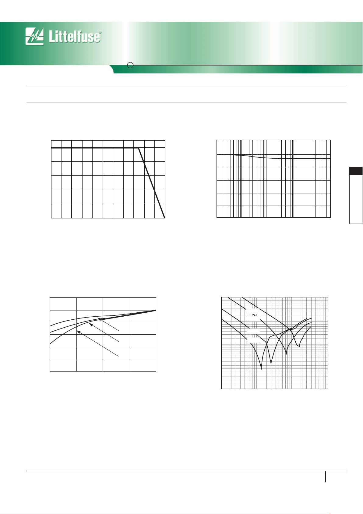
FIGURE
4. IMPEDANCE (Z) vs FREQUENCY
TYPICAL CHARACTERISTIC
0.1
FREQUENCY (MHz)
IMPEDANCE (Z)
10
100
1000
10000
1
10
100
0.01
-0402
-0603
-0805
-1206
Typical Performance Curves
For applications exceeding 1250C ambient temperature, the peak surge
current and energy ratings must be reduced as shown in Figure 1.
30
10
0.0001250.001 0.01 0.1 1
NUMBER OF PULSES
VARISTOR VOLTAGE (V)
FIGURE 3. STANDBY CURRENT AT NORMALIZED VARISTOR
VOLTAGE AND TEMPERATURE
25
20
15
10
5
85
125
O
O
O
100
80
60
40
20
0
-55 50 60 70 80 90 100 110 120 130 140 150
PERCENT OF RATED VALUE
AMBIENT TEMPERATURE (oC)
FIGURE 1. PEAK CURRENT AND ENERGY DERATING CURVE
FIGURE 2. NOMINAL VOLTAGE STABILITY TO MULTIPLE
ESD IMPULSES (8KV CONTACT DISCHARGES
PER IEC 61000-4-2)
25
0
1
CURRENT (A)
NOMINAL VOLTAGE AT 1mADC
10
100
1000
10000
5
10
15
20
30

Multilayer Transient Voltage Suppressor
MLE Varistor Series
Surface Mount Varistors
136
www.littelfuse.com
Soldering Recommendations
The principal techniques used for the soldering of components in surface
mount technology are Infrared (IR) re-flow, vapour phase re-flow, and
wave soldering. When wave soldering, the MLE suppressor is attached
to the circuit board by means of an adhesive. The assembly is then
placed on a conveyor and run through the soldering process to contact
the wave. With IR and vapour phase re-flow, the device is placed in a
solder paste on the substrate. As the solder paste is heated, it reflows
and solders the unit to the board.
The recommended solder for the MLE suppressor is a 62/36/2
(Sn/Pb/Ag), 60/40 (Sn/Pb), or 63/37 (Sn/Pb). Littelfuse also
recommends an RMA solder flux.
Wave soldering is the most strenuous of the processes. To avoid the
possibility of generating stresses due to thermal shock, a preheat stage
in the soldering process is recommended, and the peak temperature of
the solder process should be rigidly controlled. For 0402 size devices,
IR re-flow is recommended.
When using a reflow process, care should be taken to ensure that the
MLE chip is not subjected to a thermal gradient steeper than 4 degrees
per second; the ideal gradient being 2 degrees per second. During the
soldering process, preheating to within 100 degrees of the solder’s peak
temperature is essential to minimize thermal shock. Examples of the
soldering conditions for the MLE series of suppressors are given in the
tables below.
Once the soldering process has been completed, it is still necessary to
ensure that any further thermal shocks are avoided. One possible cause of
thermal shock is hot printed circuit boards being removed from the solder
process and subjected to cleaning solvents at room temperature. The
boards must be allowed to cool gradually to less than 50oC before cleaning.
Termination Options
Littelfuse offers two types of electrode termination finish for the
MLE series:
1. Silver/Platinum (standard) (Not 0402 and 0603 sizes)
2. Silver/Palladium (optional)
FIGURE 6. WAVE SOLDER PROFILE
FIGURE 7. VAPOR PHASE SOLDER PROFILE
TEMPERATURE (
o
C)
TIME (MINUTES)
300
250
200
150
100
50
0
0 0.5 1.0 1.5 2.0 2.5 3.0 3.5 4.0 4.5
MAXIMUM WAVE 260oC
SECOND PREHEAT
FIRST PREHEAT
TEMPERATURE (
o
C)
TIME (MINUTES)
250
200
150
100
50
0
0 0.5 1.0 1.5 2.0 2.5 3.0 3.5
RAMP RATE
PREHEAT ZONE
>50
o
C/s
MAXIMUM
TEMPERATURE 222
o
C
40-80
SECONDS
ABOVE 183
o
C
FIGURE 5. REFLOW SOLDER PROFILE
TEMPERATURE (
o
C)
TIME (MINUTES)
250
200
150
100
50
0
0 0.5 1.0 1.5 2.0 2.5 3.0 3.5 4.0
MAXIMUM
PREHEAT DWELL
PREHEAT ZONE
TEMPERATURE 222
o
C
RAMP RATE
<2
o
C/s
40-80
SECONDS
ABOVE 183
o
C
3. Nickel Barrier (optional for 0402-1210 package size)
(The ordering information section describes how to designate them.)

MLE Varistor Series
Surface Mount Varistors
Multilayer Transient Voltage Suppressor
137
www.littelfuse.com
3
SURFACE MOUNT
VARISTORS
Recommended Pad Outline
C
B
A
NOTE: Avoid metal runs in this area.
NOTE
DIMENSION
RECOMMENDED PAD SIZE DIMENSIONS
1206 SIZE DEVICE 0805 SIZE DEVICE 0603 SIZE DEVICE
IN MM IN MM IN MM
A 0.160 4.06 0.120 3.05 0.100 2.54
B 0.065 1.65 0.050 1.27 0.030 0.76
C 0.040 1.02 0.040 1.02 0.035 0.89
TABLE 1: PAD LAYOUT DIMENSIONS
0402 SIZE DEVICE
IN MM
0.067 1.70
0.020 0.51
0.024 0.61

Multilayer Transient Voltage Suppressor
MLE Varistor Series
Surface Mount Varistors
138
www.littelfuse.com
Standard Shipping Quantities
D
E
W
L
Mechanical Dimensions
DIMENSION
1206 SIZE 0805 SIZE 0603 SIZE
IN MM IN MM IN MM
E
0.071
L
0.02±0.01
W
0.125±0.012
DEVICE DIMENSIONS
0402 SIZE
IN MM
D Max
0.06±0.011
1.80
0.50±0.25
3.20±0.03
1.60±0.28
0.043
0.02±0.01
0.079±0.008
0.049±0.008
1.1
0.50±0.25
2.01±0.2
1.25±0.2
0.035
0.015±0.008
0.063±0.006
0.032±0.006
0.9
0.4±0.2
1.6±0.15
0.8±0.15
0.024
0.010±0.006
0.039±0.004
0.020±0.004
0.6
0.25±0.15
1.0±0.1
0.5±0.1
V 18 1206
PACKING OPTIONS
A: Bulk Pack (not 0402 size)
H: 7in (178mm) Diameter Reel
T: 13in (330mm) Diameter Reel
DEVICE SIZE:
i.e., 120 mil x 60 mil
DEVICE FAMILY
Littelfuse TVSS Device
X
MAXIMUM DC
WORKING VOLTAGE
MLE X X
CAPACITANCE OPTION
No Letter: Standard
L: Low Capacitance Version
END TERMINATION OPTION
No Letter: Ag/Pt (Standard)
W: Ag/Pd
MULTILAYER SERIES
DESIGNATOR
(3mm x 1.5mm)
(not 0402 size)
N: Nickel Barrier (0402-1210) For 0402 package size,
Nickel Barrier termination is subject to availibility.
Please contact a Littelfuse sales representative.
Ordering Information
VXXMLE TYPES
DEVICE SIZE “13” INCH REEL (“T” OPTION) “7” INCH REEL (“H” OPTION) BULK PACK (“A” OPTION)
1206 10,000 2,500 2500
0805 10,000 2,500 2500
0603 10,000 2,500 2500
0402
N/A
N/A
10,000

MLE Varistor Series
Surface Mount Varistors
Multilayer Transient Voltage Suppressor
139
www.littelfuse.com
3
SURFACE MOUNT
VARISTORS
Tape and Reel Specifications
• Conforms to EIA - 481-1, Revision A
• Can be supplied to IEC publication 286 - 3
SYMBOL DESCRIPTION
DIMENSIONS IN MILLIMETERS
A
0
Width of Cavity Dependent on Chip Size to Minimize Rotation.
B
0
Length of Cavity Dependent on Chip Size to Minimize Rotation.
K
0
Depth of Cavity Dependent on Chip Size to Minimize Rotation.
W Width of Tape 8 ±0.2
F Distance Between Drive Hole Centers and Cavity Centers 3.5 ±0.05
E Distance Between Drive Hole Centers and Tape Edge 1.75 ±0.1
P
1
Distance Between Cavity Centers 4 ±0.1
P
2
Axial Drive Distance Between Drive Hole Centers & Cavity Centers 2 ±0.1
P
0
Axial Drive Distance Between Drive Hole Centers 4 ±0.1
D
0
Drive Hole Diameter 1.55 ±0.05
D
1
Diameter of Cavity Piercing 1.05 ±0.05
T
1
0.1 Max
Top Tape Thickness
0402 Size 0603, 0805, & 1206 Sizes
2±0.05
N/A
K
0
t
1
D
0
P
0
D
1
P
1
A
0
P
2
B
0
F
E
W
PLASTIC CARRIER TAPE
EMBOSSMENT
TOP TAPE
8mm
NOMINAL
PRODUCT
IDENTIFYING
LABEL
178mm
OR 330mm
DIA. REEL
 Loading...