

Page 1
®
SIDACtor
Protection Thyristors
Broadband Optimized™ Protection
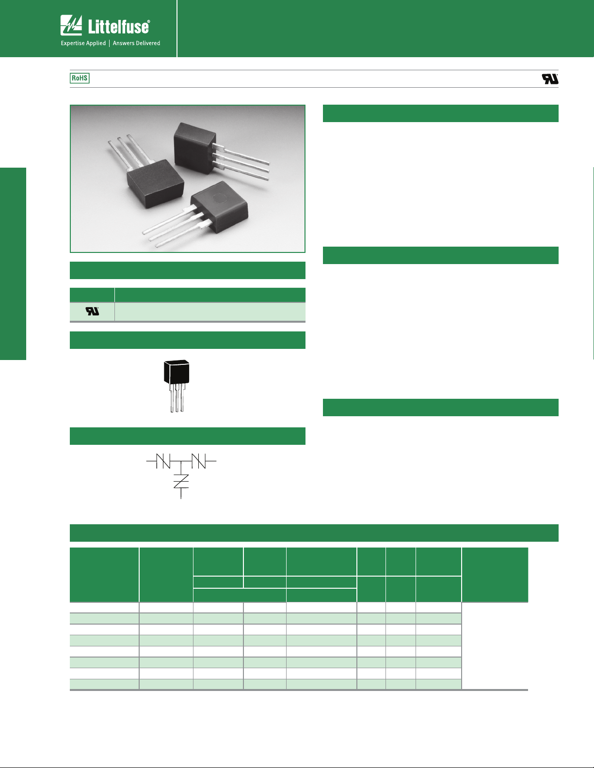
Balanced MC Series - Modified TO-220
Description
Balance MC TO-220 Series
Agency Approvals
Agency Agency File Number
E133083
Pinout Designation
PIN 1
PIN 3
PIN 2
Schematic Symbol
1
(T)
2
(G)
(R)
Balanced MC Series Modified TO-220 are low
capacitance SIDACtor
®
devices designed to protect
broadband equipment from damaging overvoltage
transients. The patented “Y” configuration also ensures
balanced overvoltage protection.
The series provides a single port solution that enables
equipment to comply with various global requlatory
standards while limiting the impact to broadband
signals.
Features and Benefits
t Low voltage overshoot
t Low on-state voltage
t Does not degrade with
use
t Fails short circuit when
surged in excess of
ratings
t Balanced overvoltage
t 40% lower capacitance
than our Baseband
Protectors, for
applications that demand
greater signal integrity
t Robust Modified TO-220
Package
t Custom lead forms
available
protection
Applicable Global Standards
t TIA-968-A
t ITU K.20/21 Enhanced
Level
3
t ITU K.20/21 Basic
t IEC 61000-4-5
t YD/T 1082
t YD/T 993
t YD/T 950
t GR 1089 Inter-building
t GR 1089 Intra-building
Electrical Characteristics
V
DRM
@l
=5μA
Part Number Marking
P1553ACMCLxx P1553ACMC 130 180 150 800 2.2 8
P1803ACMCLxx P1803ACMC 150 210 150 800 2.2 8
P2103ACMCLxx P2103ACMC 170 250 150 800 2.2 8
P2353ACMCLxx P2353ACMC 200 270 150 800 2.2 8
P2703ACMCLxx P2703ACMC 230 300 150 800 2.2 8
P3203ACMCLxx P3203ACMC 270 350 150 800 2.2 8
P3403ACMCLxx P3403ACMC 300 400 150 800 2.2 8
P5103ACMCLxx
Notes:
- Absolute maximum ratings measured at T
- Devices are bi-directional (unless otherwise noted).
- XX Part Number Suffix: ‘RP’ (Reel Pack), Blank (Bulk Pack), or ‘60’ (Type 60 lead form, Bulk Pack. Special order item -- contact factory.)
P5103ACMC
DRM
V min V max mA max
Pins 1-2, 3-2, 1-3 Pins 1-2, 3-2, 1-3
420 600 150 800 2.2 8
= 25ºC (unless otherwise noted).
A
V
S
@100V/μs
I
H
85
I
mA
max
I
S
T
A max V min
Specifications are subject to change without notice.
Please refer to www.littelfuse.com for current information.
V
T
@IT=2.2
Amps
Capacitance
See Capacitance
Values Table
© 2010 Littelfuse, Inc.
Page 2
Capacitance Values
®
SIDACtor
Protection Thyristors
Broadband Optimized™ Protection
Balance MC TO-220 Series
Part Number
pF
Pin 1-2 / 3-2
Tip-Ground, Ring-Ground
pF
Pin 1-3
Tip-Ring
MIN MAX MIN MAX
P1553ACMCLxx 30 55 20 35
P1803ACMCLxx 30 60 15 30
P2103ACMCLxx 30 45 15 30
P2353ACMCLxx 25 45 15 30
P2703ACMCLxx 25 40 15 30
P3203ACMCLxx 25 40 15 30
P3403ACMCLxx 20 35 15 25
P5103ACMCLxx 20 30 10 20
Note: Off-state capacitance (CO) is measured at 1 MHz with a 2 V bias.
Surge Ratings
I
PP
Series
0.2x310
0.5x700
1
2
2x10
2x10
1
2
8x20
1.2x50
1
2
10x160
10x160
1
2
10x560
10x560
1
2
5x320
9x720
1
2
10x360
10x360
1
2
10x10 00
10x10 00
1
2
5x310
10x700
A min A min A min A min A min A min A min A min A min A min A/μs max
C 50 500 400 200 150 200 175 100 200 30 500
Notes:
1 Current waveform in μs
2 Volt age waveform in μs
- Peak pulse current rating (IPP) is repetitive and guaranteed for the life of the product.
- IPP ratings applicable over temperature range of -40ºC to +85ºC
- The device must initially be in thermal equilibrium with -40°C < TJ < +150°C
1
2
I
TSM
50/60 Hz
di/dt
Thermal Considerations
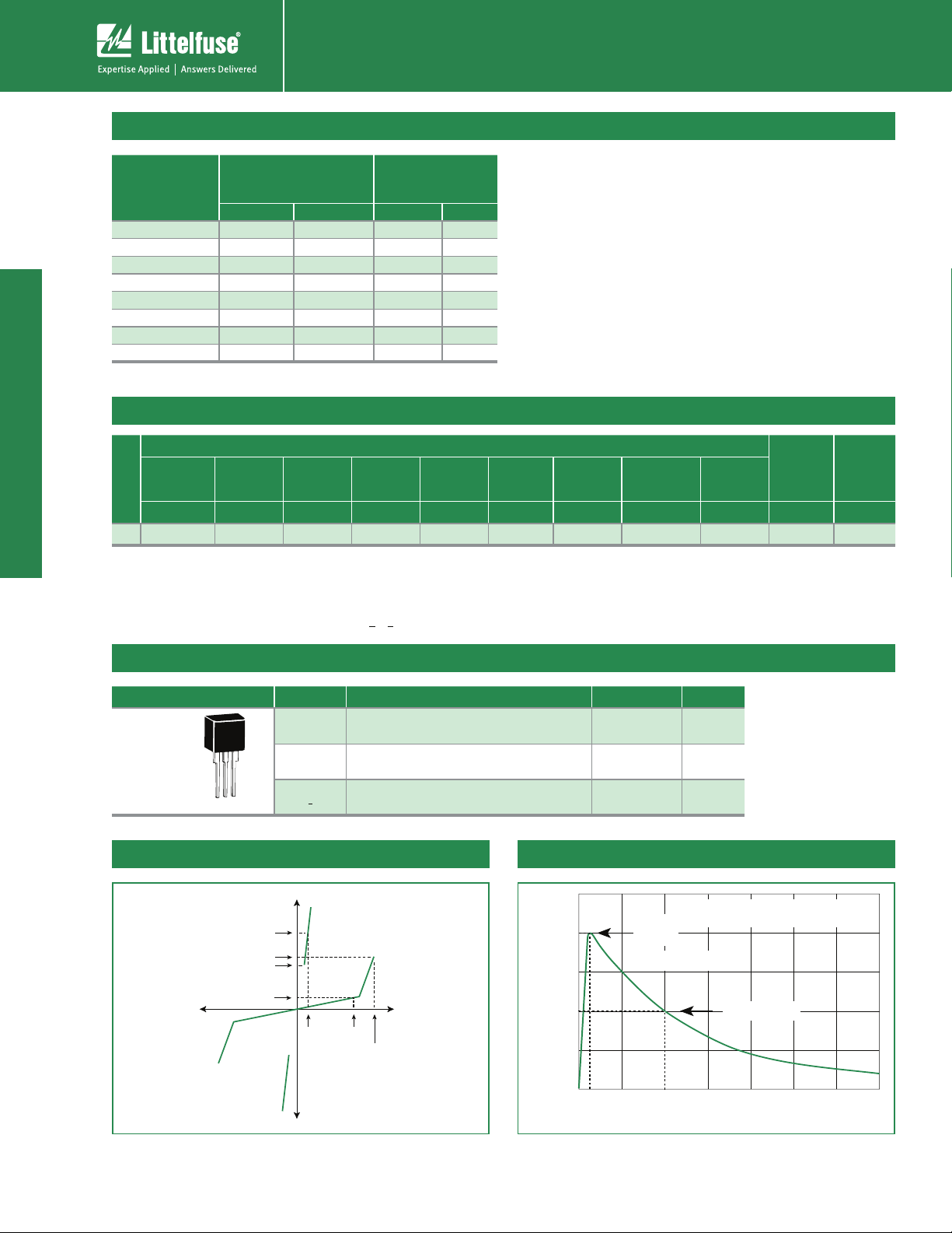
Package Symbol Parameter Value Unit
Modified
TO-220
PIN 1
PIN 3
PIN 2
V-I Characteristics
I
T
I
S
I
H
I
-V
DRM
T
T
R
Operating Junction Temperature Range -40 to +150 °C
J
Storage Temperature Range -65 to +150 °C
S
Thermal Resistance: Junction to Ambient 50 °C/ W
0JA
tr x td Pulse Waveform
+I
PP
100
Peak
Value
Waveform = t
+V
V
V
DRM
T
V
S
-I
50
– Peak Pulse Current – %I
PP
I
0
t
r
0
tr = rise time to peak value
= decay time to half value
t
d
x t
r
d
Half Value
t
d
t – Time (μs)
86
Specifications are subject to change without notice.
Please refer to www.littelfuse.com for current information.
© 2010 Littelfuse, Inc.
Page 3

®
SIDACtor
Protection Thyristors
Broadband Optimized™ Protection
Balance MC TO-220 Series
Normalized VS Change vs. Junction Temperature
14
12
10
8
6
Change – %
S
4
2
0
-4
Percent of V
-6
-8
-40 -20 0 20 40 60 80 100 120 140 160
25 °C
Junction Temperature (TJ) – °C
Soldering Parameters
Reflow Condition
Pre Heat
- Temperature Min (T
- Temperature Max (T
- Time (Min to Max) (ts)
s(min)
s(max)
)
)
Average ramp up rate (Liquidus Temp (T
to peak)
to TL - Ramp-up Rate
T
S(max)
Reflow
- Temperature (TL) (Liquidus)
- Temperature (tL)
Peak Temp (TP) +260(+0/-5)°C
Time within 5°C of actual Peak Temp (t
Ramp-down Rate 6°C/sec. Max.
Time 25°C to Peak Temp (T
)
P
Do not exceed +260°C
Pb-Free assembly
(see Fig. 1)
+150°C
+200°C
60-180 secs.
)
L
3°C/sec. Max.
3°C/sec. Max.
+217°C
60-150 secs.
)
30 secs. Max.
p
8 min. Max.
Normalized DC Holding Current vs. Case Temperature
2.0
1. 8
1. 6
H
I
= 25ºC)
1. 4
C
(T
1. 2
H
I
25°C
1. 0
0.8
Ratio of
0.6
0.4
-40 -20 0 20 40 60 80 100 120 140 160
Case Temperature (TC) - ºC
Temperature
T
S(max)
T
T
T
S(min)
25
P
L
time to peak temperature
(t 25ºC to peak)
Preheat
t
S
Figure 1
Ramp-up
t
P
Critical Zone
T
to T
L
t
L
Ramp-down
Time
P
Physical Specifications Environmental Specifications
Lead Material Copper Alloy
Terminal Finish 100% Matte-Tin Plated
Body Material
UL recognized epoxy meeting flammability
classification 94V-0
High Temp Voltage
Blocking
Temp Cycling
Biased Temp &
Humidity
High Temp Storage
Low Temp Storage -65°C, 1008 hrs.
Thermal Shock
Autoclave (Pressure
Cooker Test)
Resistance to Solder
Heat
Moisture Sensitivity
Level
87
80% Rated V
504 or 1008 hrs. MIL-STD-750 (Method 1040)
JEDEC, JESD22-A-101
-65°C to +150°C, 15 min. dwell, 10 up to 100
cycles. MIL-STD-750 (Method 1051) EIA/JEDEC,
JESD22-A104
(+85°C) 85%RH, 504 up to 1008 hrs. EIA/
52 V
DC
JEDEC, JESD22-A-101
+150°C 1008 hrs. MIL-STD-750 (Method 1031)
JEDEC, JESD22-A-101
0°C to +100°C, 5 min. dwell, 10 sec. transfer,
10 cycles. MIL-STD-750 (Method 1056) JEDEC,
JESD22-A-106
+121°C, 100%RH, 2atm, 24 up to 168 hrs. EIA/
JEDEC, JESD22-A-102
+260°C, 30 secs. MIL-STD-750 (Method 2031)
85%RH, +85°C, 168 hrs., 3 reflow cycles
(+260°C Peak). JEDEC-J-STD-020, Level 1
Specifications are subject to change without notice.
Please refer to www.littelfuse.com for current information.
(V
Peak ) +125°C or +150°C,
DRM
AC
© 2010 Littelfuse, Inc.
Page 4

®
SIDACtor
Protection Thyristors
Broadband Optimized™ Protection
Balance MC TO-220 Series
Part Numbering
xxx 3
P MC L
TYPE
P = SIDACtor
MEDIAN VOLTAGE
CONSTRUCTION VARIABLE
PACKAGE TYPE
C
A
Dimensions - Modified TO-220
A O
D
F
P
G
H
The modified TO-220 package is designed to
meet mechanical standards as set forth in
JEDEC publication number 95.
Tem pe ra t ur e
Measuremen t
Poi n t
PIN 3
PIN 2
PIN 1
L
K
J
M
N
xx
PACKING OPTIONS
Blank, RP or 60 -for Type 60 orders, contact factory
RoHS COMPLIANT
MC Series
RATING
I
PP
Inches Millimeters
Min Max Min Max
A
0.400 0.410 10.16 10.42
D
0.360 0.375 9.14 9.53
F
0.110 0.130 2.80 3.30
G
0.540 0.575 13.71 14.61
H
0.025 0.035 0.63 0.89
J
0.195 0.205 4.95 5.21
K
0.095 0.105 2.41 2.67
L
0.060 0.075 1.52 1.90
M
0.070 0.085 1.78 2.16
0.018 0.024 0.46 0.61
N
0.178 0.188 4.52 4.78
O
0.290 0.310 7.37 7.87
P
Part Marking
XXXXXXXXX
xxxxx
Part Marking Code
(Refer to Electrical Characteristics Table)
Date Code
Tape and Reel Specification — Modified TO-220
0.240
0.019
(6.10)
(0.5)
1.626
(41.15)
0.720
(18.29)
1.968
(50.0)
0.360
(9.14)
0.500
(12.7)
14.173 (360.0)
0.100
(2.54)
Dimensions are in inches
(and millimeters).
Direction of Feed
0.100
(2.54)
0.750 ± 0.010
(19.05 ± 0.25)
Packing Options
Package Type Description Quantity Added Suffix
Modified TO-220
Tape and Reel Pack
A
Modified TO-220
Bulk Pack
Modified TO-220, Type 60 Lead Form
Bulk Pack
700 RP EIA-468-B
500 N/A N/A
60
500
(special order item,
contact factory for details)
Industry Standard
N/A
88
Specifications are subject to change without notice.
Please refer to www.littelfuse.com for current information.
© 2010 Littelfuse, Inc.
 Loading...