

Page 1
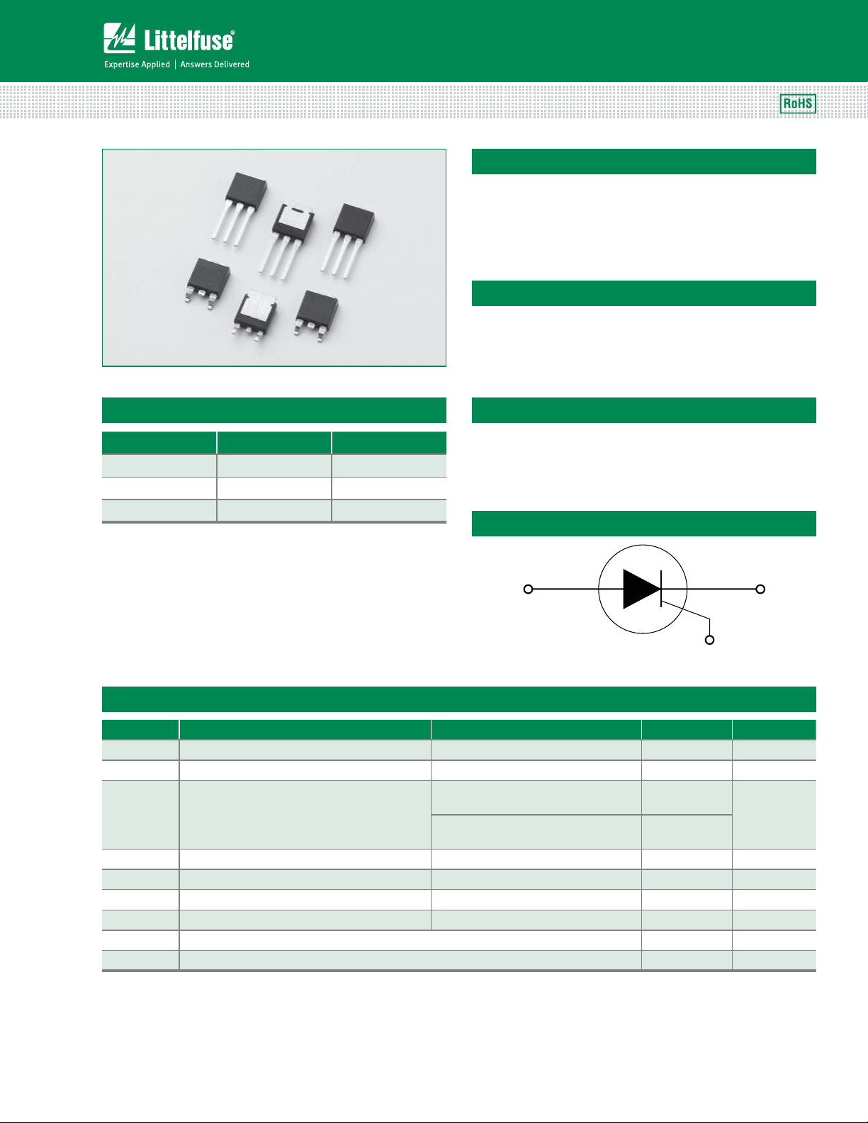
Sxx04xSx Series
Teccor® brand Thyristors
4 Amp Sensitive SCRs
Description
Excellent unidirectional switches for phase control
applications such as heating and motor speed controls.
Sensitive gate SCRs are easily triggered with microAmps
of current as furnished by sense coils, proximity switches,
and microprocessors.
Features & Benefits
t3P)4DPNQMJBOU
t(MBTToQBTTJWBUFE
junctions
t7PMUBHFDBQBCJMJUZVQ
to 600 V
t4VSHFDBQBCJMJUZVQUP
30 A
Main Features
Symbol Value Unit
I
T(RMS)
V
DRM/VRRM
I
GT
4A
400 to 600 V
50 to 500 A
Applications
Typical applications are capacitive discharge systems for
strobe lights, nailers, staplers and gas engine ignition. Also
controls for power tools, home/brown goods and white
goods appliances.
Schematic Symbol
AK
G
Absolute Maximum Ratings
Symbol Parameter Test Conditions Value Unit
I
T(RMS)
I
T(AV)
I
TSM
2
tI
I
di/dt Critical rate of rise of on-state current f = 60Hz ; T
I
GM
P
G(AV)
T
stg
T
J
RMS on-state current TC = 95°C 4 A
Average on-state current TC = 75°C 2.5 A
Peak non-repetitive surge current
2
t Value for fusing tp = 8.3 ms 3.7 A2s
single half cycle; f = 50Hz;
T
(initial) = 25°C
J
single half cycle; f = 60Hz;
T
(initial) = 25°C
J
= 110°C 50 A/s
J
25
30
Peak gate current TJ = 110°C 1 A
Average gate power dissipation TJ = 110°C 0.1 W
Storage temperature range -40 to 150 °C
Operating junction temperature range -40 to 110 °C
A
Sxx04xSx Series
235
Specifications are subject to change without notice.
©2013 Littelfuse, Inc
Revised: 09/23/13
Page 2
Teccor® brand Thyristors
4 Amp Sensitive SCRs
Electrical Characteristics — (T
Symbol Test Conditions
I
GT
V
GT
dv/dt V
V
GD
V
GRM
I
H
t
q
t
gt
Notes :
xx = voltage, x = package
(1) I
=2A; tp=50µs; dv/dt=5V/µs; di/dt=-10A/µs
T
VD = V
= 25°C, unless otherwise specified)
J
Value
Sxx04xS1 Sxx04xS2
VD = 6V; RL = 100
= V
; RGK = 1kΩ TYP. 8 V/s
D
DRM
; RL = 3.3 k; TJ = 110°C MIN. 0.2 V
DRM
MAX. 50 200 µA
MAX. 0.8 V
IGR = 10µA MIN. 6 V
IT = 20mA (initial); RGK = 1kohm MAX. 4 6 mA
(1) MAX. 50 s
IG = 2 x IGT; PW = 15µs; IT = 8A TYP. 3 4 s
Static Characteristics
Symbol Test Conditions Value Unit
V
TM
/ I
I
DRM
RRM
Note : xx or z = voltage, x = package, y = sensitivity
V
/ V
DRM
RRM
Sxx04xSy IT = 8A; tp = 380 µs MAX. 1.6 V
T
- RGK = 1kohm
= 25°C
J
= 110°C 100
T
J
MAX.
2
Unit
A
Thermal Resistances
Symbol Parameter Value Unit
R
(J-C)
R
(J-A)
Notes: xx = voltage, y = sensitivity
Junction to case (AC)
Junction to ambient Sxx04VSy 85 °C/W
Sxx04VSy 3.8
Sxx04DSy 3.0
°C/W
Sxx04xSx Series
236
Specifications are subject to change without notice.
©2013 Littelfuse, Inc
Revised: 09/23/13
Page 3
Teccor® brand Thyristors
4 Amp Sensitive SCRs
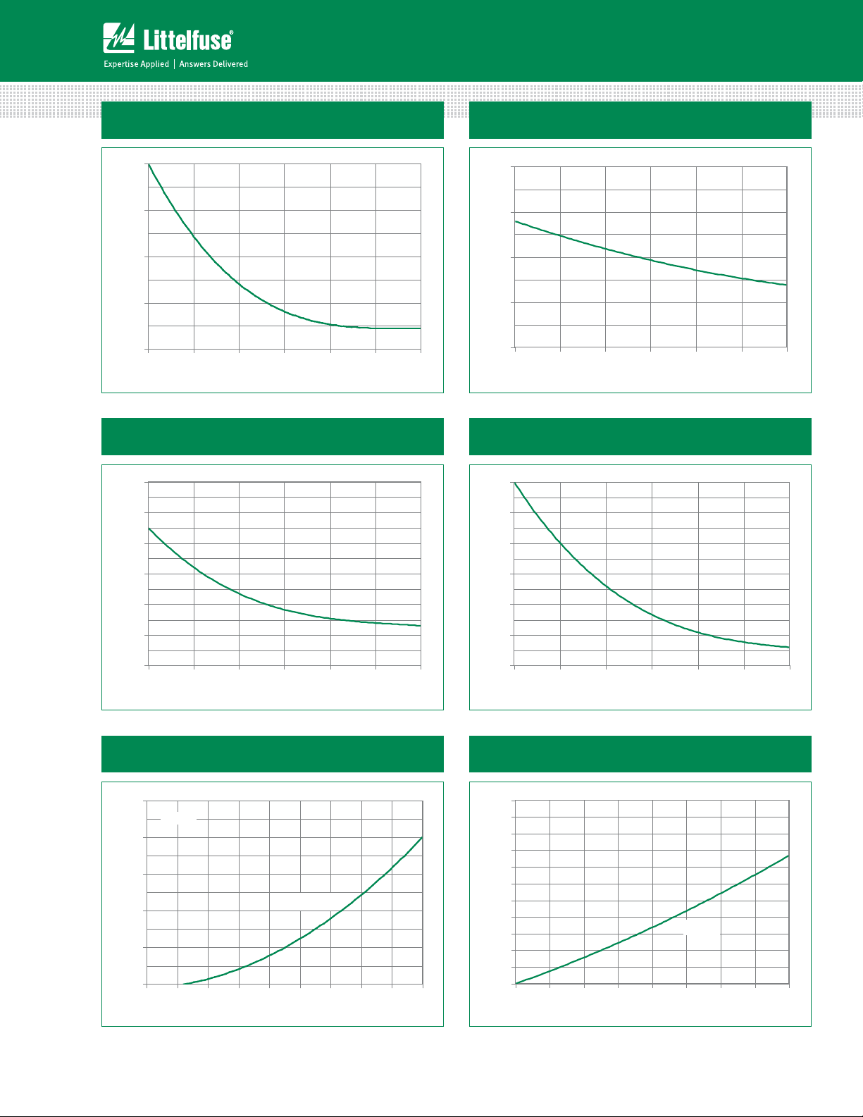
Figure 1: Normalized DC Gate Trigger Current
vs. Junction Temperature
4.0
3.0
= 25°C)
J
(T
GT
/ I
2.0
GT
Ratio of I
1.0
0.0
-40 -15 10 35 60 85 110
Junction Temperature (TJ) -- (°C)
Figure 3: Normalized DC Holding Current
vs. Junction Temperature
3.0
2.5
Figure 2: Normalized DC Gate Trigger Voltage
vs. Junction Temperature
2.0
1.5
= 25°C)
J
(T
GT
1.0
/ V
GT
0.5
Ratio of V
0.0
-40 -15 10 35 60 85 110
Junction Temperature (TJ) -- (°C)
Figure 4: Normalized DC Latching Current
vs. Junction Temperature
3.0
2.5
= 25°C)
2.0
J
(T
H
/ I
H
1.5
1.0
Ratio of I
0.5
0.0
-40 -15 10 35 60 85 110
Junction Temperature (TJ) -- (°C)
Figure 5: On-State Current vs. On-State
Voltage (Typical)
25
TJ = 25°C
20
) – Amps
T
15
Sxx04VSy
10
5
Instantaneous On-state Current (i
0
0.7 0.8 0.9 1.0 1.1 1.2 1.3 1.4 1.5 1.6
Instantaneous On-state Voltage (v) – Volts
Sxx04DSy
2.0
= 25°C)
J
(T
L
1.5
/ I
L
1.0
Ratio of I
0.5
0.0
-40 -15 10 35 60 85 110
Junction Temperature (TJ) -- (°C)
Figure 6: Power Dissipation (Typical)
vs. RMS On-State Current
5.5
5.0
4.5
] - (Watts)
4.0
D(AV)
3.5
3.0
2.5
2.0
1.5
1.0
0.5
Average On -State Po wer Dissipation [P
0.0
0.0 0.5 1.0 1.5 2.0 2.5 3. 0 3.5 4.0
RMS On -Sta te Cur rent [I
Sxx04VSy
Sxx04DSy
] - (Amps)
T(RMS)
Note: xx or z = voltage, y = sensitivity
Sxx04xSx Series
237
Specifications are subject to change without notice.
©2013 Littelfuse, Inc
Revised: 09/23/13
Page 4

Teccor® brand Thyristors
4 Amp Sensitive SCRs
Figure 7: Maximum Allowable Case Temperature
vs. RMS On-State Current
115
110
105
100
) - °C
C
95
90
85
Temperature (T
Maximum Allowable Case
80
CURRENT WAVEFORM: Sinusoidal
LOAD: Resistive or Inductive
75
CONDUCTION ANGLE: 180°
70
0.0 0.5 1.0 1. 5 2.0 2.5 3.0 3.5 4.0 4.5
RMS On-State Current [I
Sxx04VSy
Sxx04DSy
T(RMS)
] - Amps
Figure 9: Maximum Allowable Ambient Temperature
vs. RMS On-State Current
120
100
80
) -°C
60
A
(T
40
20
Maximum Allowable Ambient Temperature
0
0.0 0.2 0.4 0.6 0.8 1.0 1.2 1.4
Sxx04VSy
RMS On-State Current [I
CURRENT WAVEFORM: Sinusoidal
LOAD: Resistive or Inductive
CONDUCTION ANGLE: 180°
FREE AIR RATING
] - Amps
T(RMS)
Figure 8: Maximum Allowable Case Temperature
vs. Average On-State Current
115
110
105
100
) - °C
C
95
90
85
Temperature (T
Maximum Allowable Case
80
CURRENT WAVEFORM: Sinusoidal
LOAD: Resistive or Inductive
75
CONDUCTION ANGLE: 180°
70
0.0 0.5 1. 0 1. 5 2.0 2.5 3.0
Average On-State Current [I
Sxx04VSy
Sxx04DSy
T(AVE)
] - Amps
Figure 10: Maximum Allowable Ambient Temperature
vs. Average On-State Current
120
100
80
) -°C
A
60
40
Temperature (T
Maximum Allowable Ambient
20
0
0.0 0.2 0.4 0.6 0.8
Sxx04VSy
Average On-State Current [I
CURRENT WAVEFORM: Sinusoidal
LOAD: Resistive or Inductive
CONDUCTION ANGLE: 180°
FREE AIR RATING
] - Amps
T(AVE)
Figure 11: Peak Repetitive Capacitor Discharge Current Figure 12: Peak Repetitive Sinusoidal Pulse Current
180
160
140
) -Amps
TM
120
100
80
60
I
TRM
40
Peak Discharge Current (I
20
0
t
W
11
Note: xx = voltage, y = sensitivity
Sxx04xSx Series
1 Hz
12 Hz
60 Hz
0100
Pulse Current Duration (tW) - μs
238
180
160
140
) - Amps
TM
120
100
80
60
I
TM
40
20
Peak Discharge Current (I
0
t
W
1 10 100
Pulse Current Duration (tW) - μs
Specifications are subject to change without notice.
©2013 Littelfuse, Inc
1 Hz
12 Hz
60 Hz
Revised: 09/23/13
Page 5

Teccor® brand Thyristors
4 Amp Sensitive SCRs
Figure 13: Surge Peak On-State Current vs. Number of Cycles
100.0
Sxx04VSy
Sxx04DSy
10.0
) – Amps
TSM
1.0
Peak Surge (Non-repetitive)
On-state Current (I
0.1
1 10 100 1000
Note: xx or z - voltage, y = sensitivity
Surge Current Duration -- Full Cycles
Figure 14: Simple Test Circuit for Gate Trigger Voltage and Current
Reset
Normally-closed
Pushbutton
100
6V
+
DC
–
V1
D.U.T.
1 k
(1%)
I
GT
IN4001
I
G
V
100
GT
R1
SUPPLY FREQUENCY: 60 Hz Sinusoidal
LOAD: Resistive
RMS On-State Current: [I
Value at Specified Case Temperature
Notes:
1. Gate control may be lost during and immediately
following surge current interval.
2. Overload may not be repeated until junction
temperature has returned to steady-state
rated value.
]: Maximum Rated
T(RMS)
Note: V1 — 0 V to 10 V dc meter
V
— 0 V to 1 V dc meter
GT
I
— 0 mA to 1 mA dc milliammeter
G
R1 — 1 k potentiometer
To measure gate trigger voltage and current, raise gate
voltage (V
Gate trigger voltage is the reading on V
dropping. Gate trigger current I
the relationship
IGT = IG-
where I
dropping
Note: I
current flows out from gate lead). If negative current
occurs, I
and use I
12 µA gate products.
) until meter reading V1 drops from 6 V to 1 V.
GT
GT
V
GT
____
Amps
1000
is reading (in amperes) on meter just prior to V1
G
may turn out to be a negative quantity (trigger
GT
value is not a valid reading. Remove 1 k resistor
GT
as the more correct IGT value. This will occur on
G
just prior to V1
GT
Can be computed from
Sxx04xSx Series
239
Specifications are subject to change without notice.
©2013 Littelfuse, Inc
Revised: 09/23/13
Page 6

Soldering Parameters
Ramp-do
Teccor® brand Thyristors
4 Amp Sensitive SCRs
Reflow Condition 1Co'SFFBTTFNCMZ
T
P
- Temperature Min (T
Pre Heat
- Temperature Max (T
- Time (min to max) (ts) oTFDT
Average ramp up rate (Liquidus Temp)
(TL) to peak
T
to TL - Ramp-up Rate 5°C/second max
S(max)
Reflow
- Temperature (TL) (Liquidus) 217°C
- Temperature (tL) oTFDPOET
Peak Temperature (TP) 260
Time within 5°C of actual peak
Temperature (tp)
) 150°C
s(min)
) 200°C
s(max)
5°C/second max
+0/-5
°C
oTFDPOET
T
L
T
S(max)
Temperature
T
S(min)
25
Ramp-upRamp-up
PreheatPreheat
t
S
time to peak temperature
Ramp-down Rate 5°C/second max
Time 25°C to peak Temperature (TP) 8 minutes Max.
Do not exceed 280°C
Physical Specifications Environmental Specifications
Terminal Finish 100% Matte Tin-plated
Body Material
UL recognized epoxy meeting flammability
classification 94V-0
Lead Material Copper Alloy
Design Considerations
Careful selection of the correct device for the application’s
operating parameters and environment will go a long way
toward extending the operating life of the Thyristor. Good
design practice should limit the maximum continuous
current through the main terminals to 75% of the device
rating. Other ways to ensure long life for a power discrete
semiconductor are proper heat sinking and selection of
voltage ratings for worst case conditions. Overheating,
overvoltage (including dv/dt), and surge currents are
the main killers of semiconductors. Correct mounting,
soldering, and forming of the leads also help protect
against component damage.
Test
AC Blocking
Temperature Cycling
Temperature/
Humidity
High Temp Storage
Low-Temp Storage 1008 hours; -40°C
Thermal Shock
Autoclave
Resistance to
Solder Heat
Solderability ANSI/J-STD-002, category 3, Test A
Lead Bend MIL-STD-750, M-2036 Cond E
Specifications and Conditions
MIL-STD-750, M-1040, Cond A Applied
Peak AC voltage @ 125°C for 1008 hours ,
R
= 1kohms
GK
MIL-STD-750, M-1051,
100 cycles; -40°C to +150°C;
15-min dwell-time
EIA / JEDEC, JESD22-A101
1008 hours; 320V - DC: 85°C;
85% rel humidity
MIL-STD-750, M-1031,
1008 hours; 150°C
MIL-STD-750, M-1056
10 cycles; 0°C to 100°C; 5-min dwelltime
at each temperature; 10 sec (max) transfer
time between temperature
EIA / JEDEC, JESD22-A102
168 hours (121°C at 2 ATMs) and
100% R/H
MIL-STD-750 Method 2031
t
P
t
L
Ramp-down
Time
Sxx04xSx Series
240
Specifications are subject to change without notice.
©2013 Littelfuse, Inc
Revised: 09/23/13
Page 7

Teccor® brand Thyristors
4 Amp Sensitive SCRs
Dimensions — TO-251AA (V/I-Package) — V/I-PAK Through Hole
2
5.34
.210
Anode
A
B
C
Cathode
Anode
GATE
TC MEASURING POINT
E
D
P
Q
R
F
G
I
H
J
S
K
L
AREA: 0.040 IN
5.28
.208
Dimensions — TO-252AA (D-Package) — D-PAK Surface Mount
Dimension
Inches Millimeters
Min Typ Max Min Typ Max
A 0.037 0.040 0.043 0.94 1.01 1.09
B 0.235 0.242 0.245 5.97 6.15 6.22
C 0.350 0.361 0.375 8.89 9.18 9.53
D 0.205 0.208 0.213 5.21 5.29 5.41
E 0.255 0.262 0.265 6.48 6.66 6.73
F 0.027 0.031 0.033 0.69 0.80 0.84
G 0.087 0.090 0.093 2.21 2.28 2.36
H 0.085 0.092 0.095 2.16 2.34 2.41
I 0.176 0.180 0.184 4.47 4.57 4.67
J 0.018 0.020 0.023 0.46 0.51 0.58
K 0.035 0.037 0.039 0.90 0.95 1.00
L 0.018 0.020 0.023 0.46 0.52 0.58
P 0.042 0.047 0.052 1.06 1.20 1.32
Q 0.034 0.039 0.044 0.86 1.00 1.11
R 0.034 0.039 0.044 0.86 1.00 1.11
S 0.074 0.079 0.084 1.86 2.00 2.11
Anode
A
B
C
Cathode
Anode
E
MEASURING POINT
T
C
D
P
Q
GATE
F
G
I
L
O
N
AREA
M
5.28
.208
2
: 0.040 IN
K
5.34
.210
J
1.60
.063
3
.118
H
6.71
.264
4.60
.181
6.71
.264
1.80
.071
Dimension
A
Inches Millimeters
Min Typ Max Min Typ Max
0.037 0.040 0.043 0.94 1.01 1.09
B 0.235 0.243 0.245 5.97 6.16 6.22
C 0.106 0.108 0.113 2.69 2.74 2.87
D 0.205 0.208 0.213 5.21 5.29 5.41
E 0.255 0.262 0.265 6.48 6.65 6.73
F 0.027 0.031 0.033 0.69 0.80 0.84
G 0.087 0.090 0.093 2.21 2.28 2.36
H 0.085 0.092 0.095 2.16 2.33 2.41
I 0.176 0.179 0.184 4.47 4.55 4.67
J 0.018 0.020 0.023 0.46 0.51 0.58
K
0.035 0.037 0.039 0.90 0.95 1.00
L 0.018 0.020 0.023 0.46 0.51 0.58
M 0.000 0.000 0.004 0.00 0.00 0.10
N 0.021 0.026 0.027 0.53 0.67 0.69
O 0°0°5°0°0°5°
P 0.042 0.047 0.052 1.06 1.20 1.32
Q 0.034 0.039 0.044 0.86 1.00 1.11
Sxx04xSx Series
241
Specifications are subject to change without notice.
©2013 Littelfuse, Inc
Revised: 09/23/13
Page 8

Product Selector
Teccor® brand Thyristors
4 Amp Sensitive SCRs
Part Number
400V 600V 800V 1000V
Voltage
Gate Sensitivity Type Package
Sxx04DS1 X X 50A Sensitive SCR TO-252
Sxx04DS2 X X 200A Sensitive SCR TO-252
Sxx04VS1 X X 50A Sensitive SCR TO-251
Sxx04VS2 X X 200A Sensitive SCR TO-251
Note: xx = Voltage
Packing Options
Part Number Marking Weight Packing Mode Base Quantity
Sxx04DSyTP Sxx04DSy 0.3g Tube 750 (75 per tube)
Sxx04DSyRP Sxx04DSy 0.3g Embossed Carrier 2500
Sxx04VSyTP Sxx04VSy 0.4g Tube 750 (75 per tube)
Note: xx = voltage, y = sensitivity
TO-252 Embossed Carrier Reel Pack (RP) Specs
0.059
DIA
(1.5)
Gate Cathode
DC
DC
XX
XXXXXX
XX
XXXXXX
0.63
(16.0)
0.524
(13.3)
0.157
(4.0)
*
XXXXXX
XX
DC
XXXXXX
Part Marking System
TO-251AA- (V Package)
TO-252AA- (D Package)
L6004V4
L6004V4
Cover tape
*
0.512 (13.0)
Arbor Hole
Diameter
0.64
(16.3)
0.315
(8.0)
12.99
(330.0)
Anode
Dimensions
are in inches
(and millimeters).
Direction of Feed
YMLDD
Date Code Marking
Y:Year Code
M: Month Code
L: Location Code
DD: Calendar Code
®
Part Numbering System
SS160 04 V
DEVICE TYPE
S: SCR
VOLTAGE RATING
4: 400V
6: 600V
CURRENT RATING
04: 4A
YMLDD
®
SENSITIVITY & TYPE
AS1: 50
μ
S2: 200 A
μ
PACKAGE TYPE
V: TO-251 (V/I-Pak)
D: TO-252 (D-Pak)
Sxx04xSx Series
242
Specifications are subject to change without notice.
©2013 Littelfuse, Inc
Revised: 09/23/13
 Loading...