

Page 1

TVS Diode Arrays (SPA
VCC
10/100
Ethernet
PHY
TX +
TX -
RX +
RX -
VCC
GND
SRV05-4HTG
TX +
TX -
RX +
RX -
Unused
Unused
Unused
RJ45
Unused
To Twisted-Pair Network
75
75
75
75
1
2
3
6
5
4
10/100 Ethernet Differential Protection
®
Diodes)
Lightning Surge Protection - SRV05 Series
SRV05 Series 6V 10A Diode Array
Pinout
I/O 1
GND
I/O 2
Functional Block Diagram
Additional Information
Datasheet
Life Support Note:
Not Intended for Use in Life Support or Life Saving Applications
The products shown herein are not designed for use in life sustaining or life saving
applications unless otherwise expressly indicated.
6
1
5
2
Resources
4
3
I/O 4
V
CC
I/O 3
Samples
RoHS
Pb
GREEN
Description
The SRV05 integrates low capacitance rail-to-rail diodes with
an additional zener diode to protect each I/O pin against
ESD and high surge events. This robust device can safely
absorb surge current per IEC61000-4-5 (t
=8/20µs) without
P
performance degradation and a minimum ±20kV ESD
per IEC61000-4-2. Their very low loading capacitance also
makes them ideal for protecting high speed signal pins.
Features
• ESD, IEC61000-4-2,
±20kV contact, ±30kV air
• EFT, IEC61000-4-4, 40A
(5/50ns)
• Lightning, IEC61000-4-5,
10A (8/20μs)
• Low capacitance of 2pF
(TYP) per I/O
• Low leakage current of
0.5μA (MAX) at 5V
• Small SOT23-6 (
MO-178) packaging
JEDEC
Applications
• LCD/PDP TVs
• Monitors
• Notebooks
• 10/100/1000 Ethernet
• Firewire
• Set Top Boxes
• Flat Panel Displays
• Portable Medical
Application Examples
USB
Controller
10/100/1000
Ethernet
PHY
USB Dual Port Protection
C
T
C
T
10/100/1000 Ethernet Protection
TX +
TX -
RX +
RX -
VCC
GND
R
T
R
T
C
T
R
T
R
T
C
T
1
2
3
SRV05-4HTG
VCC
6
5
4
V
BUS
SRV05-4HTG
V
BUS
V
BUS
D +
USB
D -
Port
GND
V
BUS
V
BUS
D +
USB
Port
D -
GND
RJ45
Unused
Unused
TX +
TX -
RX +
RX -
To Twisted-Pair Network
Unused
Unused
75
75
75
75
© 2013 Littelfuse, Inc.
Specifications are subject to change without notice.
Revised: 11/25/13
Page 2
TVS Diode Arrays (SPA
®
Diodes)
Lightning Surge Protection - SRV05 Series
Absolute Maximum Ratings
Symbol Parameter Value Units
OP
V
C
I/O-GND
C
1
=25ºC)
RWM
R
LEAK
V
C
DYN
ESD
I/O-I/O
10 A
IR ≤ 1µA 6.0 V
IR = 1mA 8.0 V
VR=5V 0.1 0.5 µA
IPP=1A, tp=8/20µs, I/O to GND
I
=5A, tp=8/20µs, I/O to GND
PP
I
=8A, tp=8/20µs, I/O to GND
PP
(VC2 - VC1) / (I
IEC61000-4-2 (Contact) ±20 kV
IEC61000-4-2 (Air) ±30 kV
Reverse Bias=0V 2.4 3.0 pF
Reverse Bias=1.65V 2.0 pF
Reverse Bias=0V 1. 2 pF
I
PP
P
PK
T
OP
T
STOR
CAUTION: Stresses above those listed in “Absolute Maximum Ratings” may cause
permanent damage to the device. This is a stress only rating and operation of the device
at these or any other conditions above those indicated in the operational sections of this
specification is not implied.
1
Non-repetitive pulse per waveform on page 3
Peak Current (tp=8/20μs)
Peak Pulse Power (tp=8/20μs) 150 W
Operating Temperature –40 to 125 °C
Storage Temperature –55 to 150 °C
Electrical Characteristics (T
Parameter Symbol Test Conditions Min Typ Max Units
Reverse Standoff Voltage V
Reverse Voltage Drop V
Reverse Leakage Current I
Clamp Voltage
Dynamic Resistance R
ESD Withstand Voltage
Diode Capacitance
Diode Capacitance
Notes: 1 Parameter is guaranteed by design and/or device characterization.
2
Repetitive pulse per waveform on page 3.
1
1
1
1
Thermal Information
Parameter Rating Units
Storage Temperature Range –55 to 150 °C
Maximum Junction Temperature 150 °C
Maximum Lead Temperature
(Soldering 20-40s)
2
2
2
- I
) 0.7 Ω
PP2
PP1
8.8 10.0 V
11. 5 13.0 V
13.2 15.0 V
260 °C
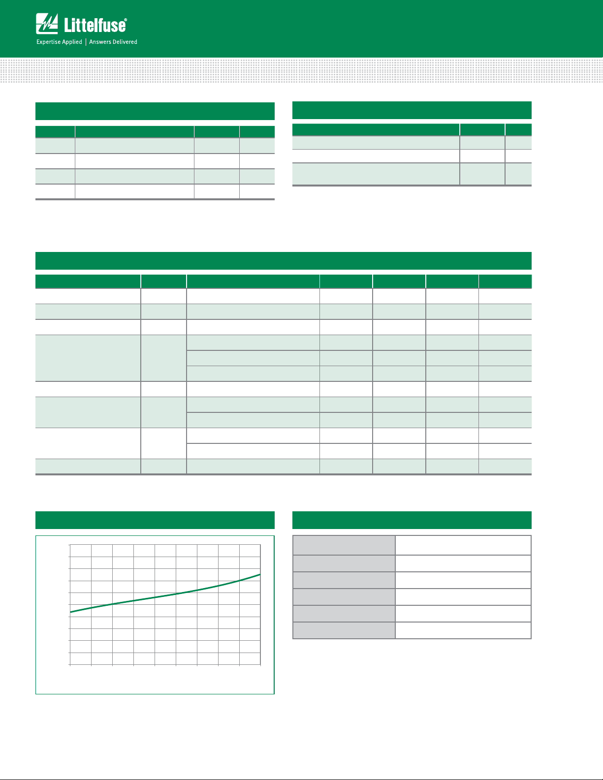
Clamping Voltage vs. I
20.0
18.0
16.0
)
14.0
C
12.0
10.0
8.0
6.0
Clamp Voltage (V
4.0
2.0
0.0
1 2 3 4 5 6 7 8 9 10
PP
Peak Pulse Current-IPP (A)
Product Characteristics
Lead Plating Matte Tin
Lead Material Copper Alloy
Lead Coplanarity 0.0004 inches (0.102mm)
Substitute Material Silicon
Body Material Molded Epoxy
Flammability UL 94 V-0
Notes :
1. All dimensions are in millimeters
2. Dimensions include solder plating.
3. Dimensions are exclusive of mold ash & metal burr.
4. Blo is facing up for mold and facing down for trim/form, i.e. reverse trim/form.
5. Package surface matte nish VDI 11-13.
Specifications are subject to change without notice.
© 2013 Littelfuse, Inc.
Revised: 11/25/13
Page 3

TVS Diode Arrays (SPA
0.0
0.5
1.0
1.5
2.0
2.5
3.0
0.0 0.5 1.0 1.5 2.0 2.5 3.0 3.5 4.0 4.5 5.0
DC Bias (V)
Capacitance (pF)
VCC=Float
V
CC
=5V
V
CC
=3.3V
0%
10%
20%
30%
40%
50%
60%
70%
80%
90%
100%
110%
0.0 5.0 10.0 15.0 20.0 25.0 30.0
Time (μs)
Percent of I
PP
t
R
R
o
C
e
T
T
L*4
L * 4
Product Series
L = SRV05
Number of Channels
Assembly Site
(Varies)
L = S
(Varies)
®
Diodes)
Lightning Surge Protection - SRV05 Series
Pulse WaveformCapacitance vs. Reverse Bias
Soldering Parameters
Reflow Condition Pb – Free assembly
Pre Heat
- Temperature Min (T
- Temperature Max (T
) 150°C
s(min)
) 200°C
s(max)
- Time (min to max) (ts) 60 – 180 secs
Average ramp up rate (Liquidus) Temp
(T
) to peak
L
to TL - Ramp-up Rate 3°C/second max
T
S(max)
Reflow
- Temperature (TL) (Liquidus) 217°C
- Temperature (tL) 60 – 150 seconds
Peak Temperature (TP) 260
Time within 5°C of actual peak
Temperature (t
)
p
3°C/second max
+0/-5
°C
20 – 40 seconds
Ramp-down Rate 6°C/second max
Time 25°C to peak Temperature (T
) 8 minutes Max.
P
Do not exceed 260°C
Part Numbering System
SRV05
–
4
H T
G
T
P
T
L
T
S(max)
Temperature
T
S(min)
25
time to peak temperature
Part Marking System
t
S
PreheatPrehea
Ramp-up
amp-up
t
P
t
L
Critical Zone
ritical Zon
L to TP
to
T
Ramp-down
amp-d
Time
Series
Number of
Channels
© 2013 Littelfuse, Inc.
Specifications are subject to change without notice.
Revised: 11/25/13
G= Green
T= Tape & Reel
Package
H: SOT23-6
Ordering Information
Part Number Package Marking Min. Order Qty.
SRV05-4HTG SOT23-6 L*4 3000
Page 4

Package Dimensions — SOT23-6
Recommended Solder Pad Layout
P
R
TVS Diode Arrays (SPA
®
Diodes)
Lightning Surge Protection - SRV05 Series
Package SOT23-6
Pins 6
JEDEC MO-178
A 0.900 1.450 0.035 0.057 -
A1 0.000 0.150 0.000 0.006 -
A2 0.900 1.300 0.035 0.051 -
b 0.350 0.500 0.0138 0.0196 -
C 0.080 0.220 0.0031 0.009 -
D 2.800 3.000 0.11 0.118 3
E 2.600 3.000 0.102 0.118 -
E1 1.500 1.750 0.06 0.069 3
e 0.95 Ref 0.0374 ref -
e1 1.9 Ref 0.0748 Ref -
L 0.100 0.600 0.004 0.023 4,5
N 6 6 6
a 0º 10 º 0º 10 º -
M 2.590 0.102 -
O 0.690 .027 TYP -
P 0.990 .039 TYP -
M
R 0.950 0.038 -
Notes:
1. Dimensioning and tolerances per ANSI 14.5M-1982.
2. Package conforms to EIAJ SC-74 (1992).
3. Dimensions D and E1 are exclusive of mold ash, protrusions, or gate burrs.
4. Footlenth L measured at reference to seating plane.
5. “L” is the length of at foot surface for soldering to substrate.
6. “N” is the number of terminal positions.
7. Controling dimension: MILLIMETER. Converted inch dimensions are not necessarily exact.
Millimeters Inches
Min Max Min Max
Notes
Embossed Carrier Tape & Reel Specification — SOT23-6
8mm TAPE AND REEL
ACCESS HOLE
180mm
14.4mm
13mm
60mm
8.4mm
DIA. HOLE
8mm
1.5mm
SOT-23 (8mm POCKET PITCH)
USER DIRECTION OF FEED
4.0mm
4.0mm
2.0mm
PIN 1
1.75mm
C
L
GENERAL INFORMATION
1. 3000 PIECES PER REEL.
2. ORDER IN MULTIPLES OF FULL REELS ONLY.
3. MEETS EIA-481 REVISION "A" SPECIFICATIONS.
Specifications are subject to change without notice.
© 2013 Littelfuse, Inc.
Revised: 11/25/13
 Loading...