

TVS Diode Arrays (SPA
GND (PIN 1)
PIN 4
PIN 2
PIN 3
RoHS
GREEN
SOT143
®
Diodes)
Lightning Surge Protection- SR05 Series
SR05 Series 5V 25A Diode Array
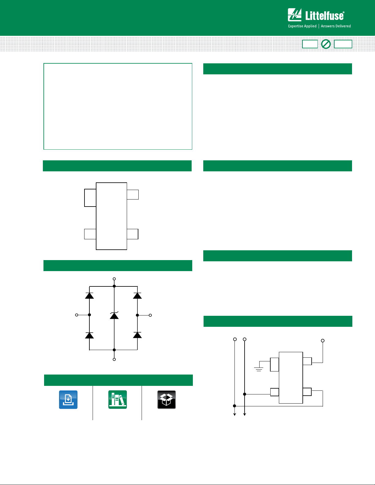
Pinout
GND
I/O 1
Vcc
I/O 2
Pb
Description
The SR05 consists of four, low capacitance steering diodes
and a low voltage TVS diode that provide protection against
ESD and lightning surge events. Each channel or I/O pin
can safely absorb up to 25A (tp=8/20μs) and repetitive ESD
strikes above the maximum level (Level 4) specified in the
IEC 61000-4-2 international standard without performance
degradation.
The low loading capacitance makes it ideal for protecting
high-speed telecommunication data lines.
Features
• ESD, IEC61000-4-2 ,
±30kV contact discharge,
±30kV air discharge
• EFT, IEC61000-4-4, 80A
(t
=5/50ns)
p
• Lightning protection,
IEC61000-4-5, 25A
(t
=8/20µs)
p
• Low capacitance of 6.0pF
(TYP) per I/O
• Low clamp voltage
• Small SOT143 (JEDEC TO-
253) packaging
Functional Block Diagram
Additional Information
Datasheet
Life Support Note:
Not Intended for Use in Life Support or Life Saving Applications
The products shown herein are not designed for use in life sustaining or life
saving applications unless otherwise expressly indicated.
Resources
Samples
Applications
• T1/E1 IC/Secondary
Protection
• Ethernet 10BaseT
• WAN/LAN Equipment
• ISDN S/T Interface
• Video Lines
• Microcontroller Input
Protection
Application Example
I/O
I/O
1
2
The SR05 integrates a TVS Diode between the Vcc and Gnd
pins. This allows the array to protect the power supply
against ESD and lighting surges when these pins are both
connected in the application.
V
CC
4
3
© 2013 Littelfuse, Inc.
Specifications are subject to change without notice.
Revised: 04/24/13
TVS Diode Arrays (SPA
05
0%
10%
20%
30%
40%
50%
60%
70%
80%
90%
100%
110%
0.05.0 10.0 15.0 20.0 25.0 30.0
Time (μs)
Percent of I
PP
®
Diodes)
Lightning Surge Protection- SR05 Series
Absolute Maximum Ratings
Symbol Parameter Value Units
I
PP
P
Pk
T
OP
T
STOR
CAUTION: Stresses above those listed in “Absolute Maximum Ratings” may cause
permanent damage to the device. This is a stress only rating and operation of the device
at these or any other conditions above those indicated in the operational sections of this
specification is not implied.
Electrical Characteristics (T
Reverse Stand-Off Voltage V
Reverse Leakage Current I
Reverse Breakdown Voltage V
Clamping Voltage, Line-Ground
Clamping Voltage, Line-Ground
Clamping Voltage, Line-Ground
Dynamic Resistance, Line-Ground
ESD Withstand Voltage
Diode Capacitance
Note: 1. Parameter is guaranteed by design and/or device characterization.
Peak Current (tp=8/20μs) 25.0 A
Peak Pulse Power (tp=8/20μs) 450 W
Operating Temperature –40 to 125 °C
Storage Temperature –55 to 150 °C
=25ºC)
OP
Parameter Symbol Test Conditions Min Typ Max Units
RWM
R
BR
1
V
1
V
1
V
1
1
1
R
V
C
C
I/O-GND
C
C
C
DYN
ESD
I/O-I/O
VR= 5V, I/O to GND - - 5.0 µA
It = 1mA 6.0 - - V
IPP= 1A, tp=8/20 µs - - 9.8 V
IPP= 10A, tp=8/20 µs - - 12.0 V
IPP= 25A, tp=8/20 µs - - 18.0 V
( VC2-VC1)/(I
IEC61000-4-2 (Contact Discharge) ±30 - - kV
IEC61000-4-2 (Air Discharge) ±30 kV
Reverse Bias=0V - 3.0 - pF
Reverse Bias=0V - 6.0 10.0 pF
Thermal Information
Parameter Rating Units
Storage Temperature Range –55 to 150 °C
Maximum Junction Temperature 150 °C
Maximum Lead Temperature
(Soldering 20-40s)
- - 5.0 V
) - 0.3 -
PP2-IPP1
260 °C
W
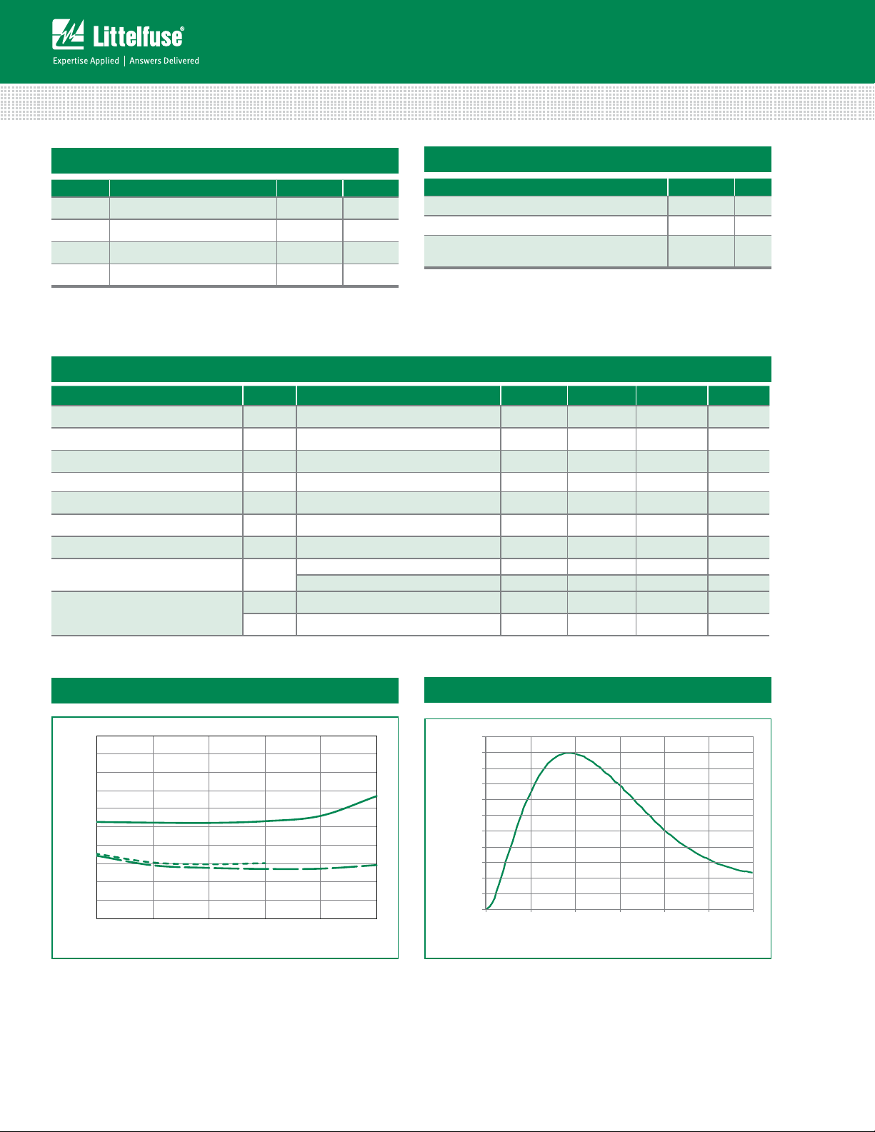
Capacitance vs. Reverse Bias
10.0
9.0
8.0
7.0
6.0
5.0
4.0
Capacitance (pF)
3.0
2.0
1.0
0.0
0.01.0 2.03.0 4.
Vcc=3.3V
Reverse Bias (V)
Vcc Open
Vcc=5V
Pulse Waveform
.0
Specifications are subject to change without notice.
© 2013 Littelfuse, Inc.
Revised: 04/24/13
 Loading...