

Littelfuse SP723 User Manual
TVS Diode Arrays (SPA
V+
IN
RoHS
GREEN
®
Diodes)
General Purpose ESD Protection - SP723 Series
SP723 Series 5pF 8kV Diode Array
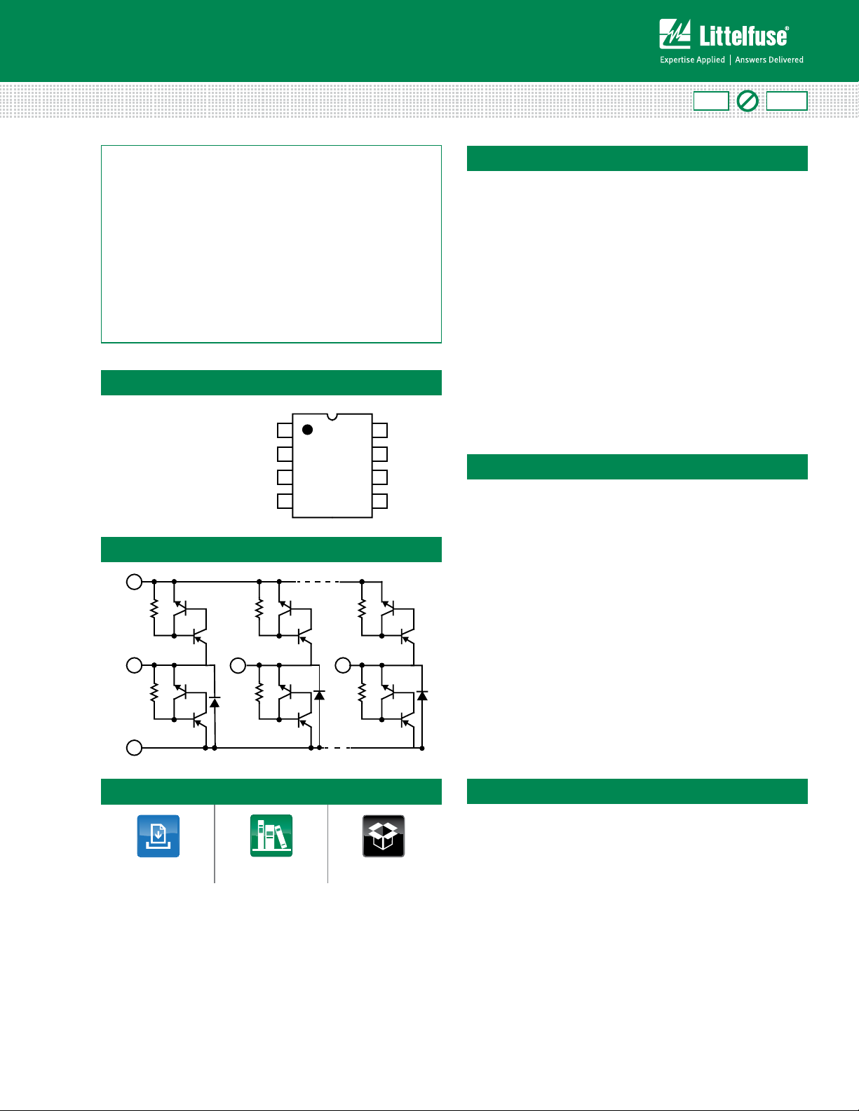
Pinout
SP723 (PDIP, SOIC)
TOP VIEW
Functional Block Diagram
8
1
4
V-
2
IN
1
IN
2
IN
3
IN
4
V-
3, 5-7
IN
8
7
6
5
V+
IN
IN
IN
Pb
Description
The SP723 is an array of SCR/Diode bipolar structures for
ESD and over-voltage protection of sensitive input circuits.
The SP723 has 2 protection SCR/Diode device structures
per input. There are a total of 6 available inputs that can be
used to protect up to 6 external signal or bus lines. Overvoltage protection is from the IN (Pins 1 - 3 and Pins 5 - 7)
to V+ or V-.
The SCR structures are designed for fast triggering at a
threshold of one +V
a -V
diode threshold below V- (Pin 4). From an IN input,
BE
a clamp to V+ is activated if a transient pulse causes the
input to be increased to a voltage level greater than one
V
above V+. A similar clamp to V- is activated if a negative
BE
pulse, one V
less than V-, is applied to an IN input.
BE
Refer to Fig 1 and Table 1 for further details. Refer to
Application Note AN9304 and AN9612 for further detail.
Features
• ESD Interface per HBM Standards
- IEC 61000-4-2, Direct Discharge .......... 8kV (Level 4)
- IEC 61000-4-2, Air Discharge ...............15kV (Level 4)
- MIL-STD-3015.7 .................................................25kV
• Peak Current Capability
- IEC 61000-4-5 8/20µs Peak Pulse Current .......... ±7A
- Single Transient Pulse, 100µs Pulse Width ......... ±4A
• Designed to Provide Over-Voltage Protection
- Single-Ended Voltage Range to ........................ +30V
- Differential Voltage Range to ............................ ±15V
• Fast Switching ..............................................2ns Risetime
• Low Input Leakages ............................2nA at 25ºC Typical
• Low Input Capacitance .....................................5pF Typical
• An Array of 6 SCR/Diode Pairs
• Operating Temperature Range....................-40ºC to 105ºC
diode threshold above V+ (Pin 8) or
BE
Additional Information
Datasheet
Life Support Note:
Not Intended for Use in Life Support or Life Saving Applications
The products shown herein are not designed for use in life sustaining or life saving
applications unless otherwise expressly indicated.
© 2013 Littelfuse, Inc.
Specifications are subject to change without notice.
Revised: 04/24/13
Resources
Samples
Applications
• Microprocessor/Logic
Input Protection
• Data Bus Protection
• Analog Device Input
Protection
• Voltage Clamp
TVS Diode Arrays (SPA
®
Diodes)
General Purpose ESD Protection - SP723 Series
Absolute Maximum Ratings
Parameter Rating Units
Continuous Supply Voltage, (V+) - (V-) +35 V
Forward Peak Current, IIN to VCC, IIN to
GND (Refer to Figure 5)
Peak Pulse Current, 8/20µs ±7 A
CAUTION: Stresses above those listed in “Absolute Maximum Ratings” may cause
permanent damage to the device. This is a stress only rating and operation of the device
at these or any other conditions above those indicated in the operational sections of this
specification is not implied.
Note:
ESD Ratings and Capability (Figure 1, Table 1)
Load Dump and Reverse Battery (Note 2)
Electrical Characteristics T
= -40oC to 105oC, V
A
±4, 100µs A
= 0.5VCC , Unless Otherwise Specified
IN
Thermal Information
Parameter Rating Units
Thermal Resistance (Typical, Note 1) θ
PDIP Package 160
SOIC Package 170
Storage Temperature Range -65 to 150
Maximum Junction Temperature (Plastic
Package)
Lead Temperature
(Soldering 20-40s) (SOIC Lead Tips Only)
is measured with the component mounted on an evaluation PC board in free air.
1. θ
JA
JA
150
260
o
C/W
o
C/W
o
C/W
o
C
o
C
o
C
Parameter Symbol Test Conditions Min Typ Max Units
Operating Voltage Range,
V
=[(V+)-(V-)]
SUPPLY
V
SUPPLY
- 2 to 30 - V
Forward Voltage Drop
IN to V- V
IN to V+ V
Input Leakage Current I
Quiescent Supply Current I
QUIESCENT
FWDL
FWDH
IN
IIN=2A(Peak Pulse) - 2 - V
- 2 - V
-20 5 20 nA
- 50 200 nA
Equivalent SCR ON Threshod Note 3 - 1. 1 - V
Equivalent SCR ON Resistance V
Input Capacitance C
Input Switching Speed t
Notes:
2. In automotive ans battery operated systems, the power supply lines should be externally protected for load dump and reverse battery. When the V+ and V- Pins are connected to the same
supply voltage source as the device or control line under protection, acurrent limiting resistor should be connectied in series between the external supply and the SP723 supply pins to
limit reverse battery current to within the rated maximum limits. Bypass capacitors of typically 0.01µF or larger from the V+ and V- Pins to ground are recommended.
3. Refer to the Figure 3 graph for determine peak current and dessipation under EOS conditions.
IN
ON
; Note 3 - 0.5 - Ω
FWD/IFWD
- 5 - PF
- 2 - ns
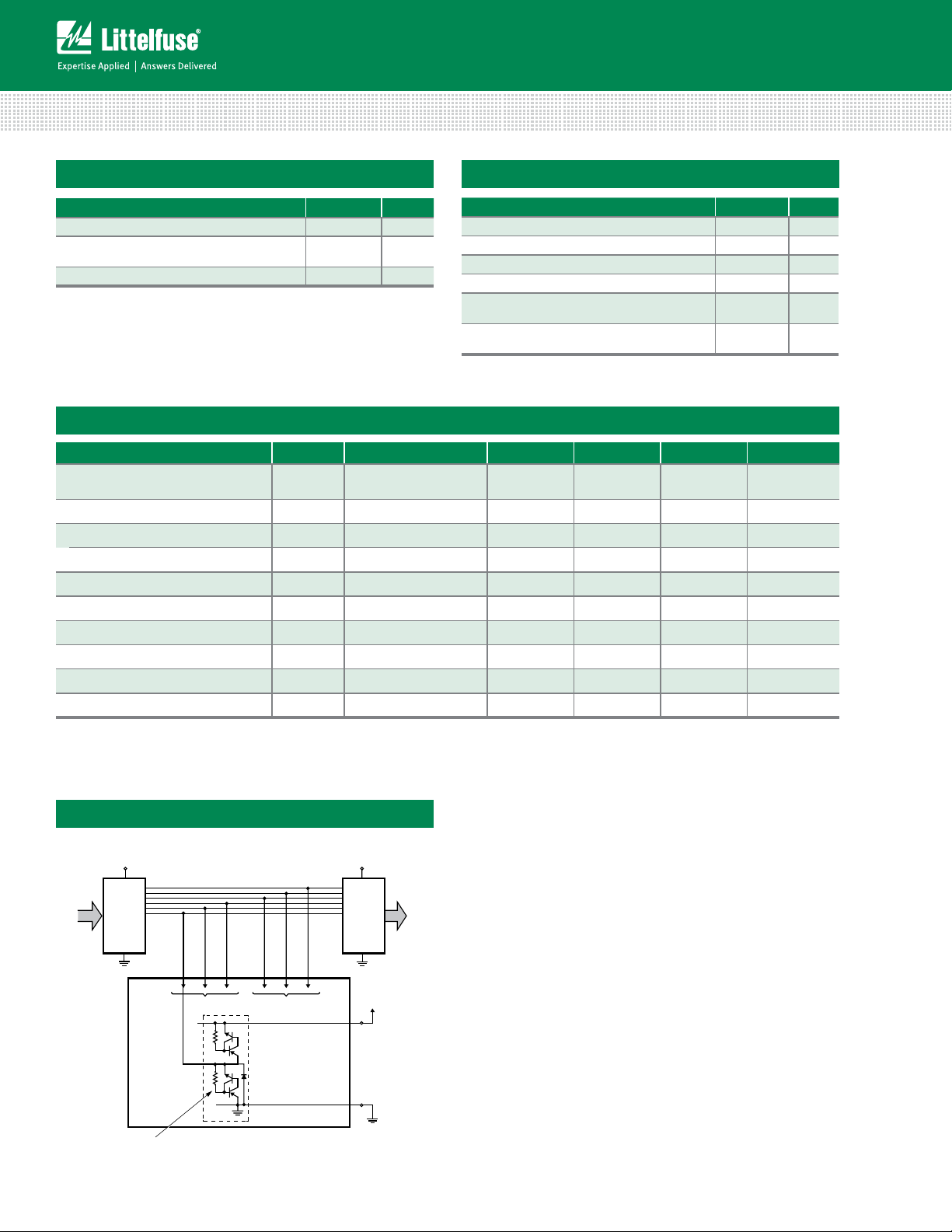
Typical Application of the SP723
(Application as an Input Clamp for Over-voltage, Greater than 1VBE
Above V+ or less than -1VBE below V-)
+V
CC
INPUT
DRIVERS
OR
SIGNAL
SOURCES
SP723
SP723 INPUT PROTECTION CIRCUIT (1 OF 6 SHO WN)
IN 5 - 7IN 1 - 3
+V
LINEAR OR
DIGITAL IC
INTERFACE
TO +V
V+
V-
CC
CC
Specifications are subject to change without notice.
© 2013 Littelfuse, Inc.
Revised: 04/24/13
 Loading...