

TVS Diode Arrays (SPA
5
8
1
4
1
6
7
12
GND
GND
SP6003-04UTG-1
SP6003-06UTG-1
µDFN-08
µDFN-12
Cd Cd
18
Cd Cd
27
Cd Cd
36
Cd Cd
45
Cd Cd
1
12
Cd Cd
2
11
Cd Cd
3
10
Cd Cd
4
9
Cd Cd
5
8
Cd Cd
67
SP6003-04UTG-1
SP6003-06UTG-1
Dx: SP6003-04 Silicon Protection Array
®
Diodes)
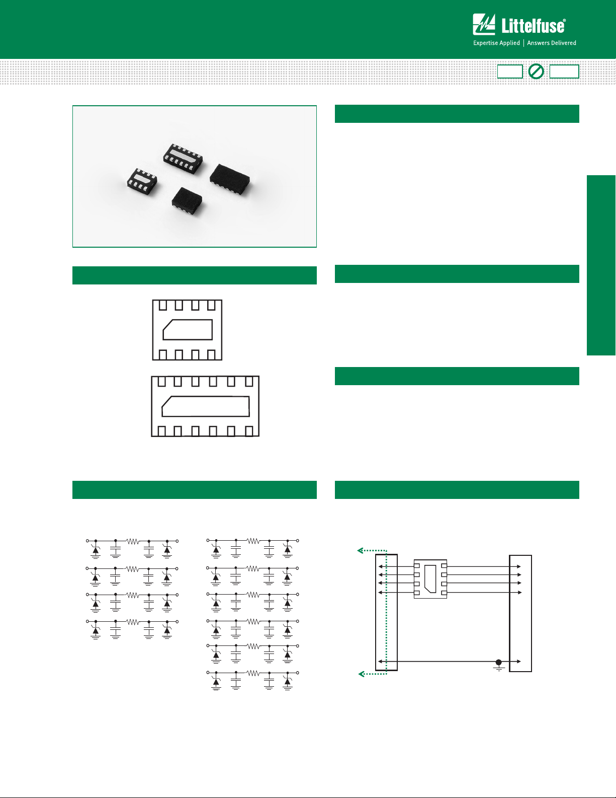
ESD and EMI Filter Devices - SP6003 Series
SP6003 Series 7pF EMI Filter Array with ESD Protection
Description
Littelfuse’s SP6003 integrates 4 and 6 EMI filters (C-R-C)
into a small, low-profile µDFN package with each filter
providing greater than -20dB attenuation at 1GHz.
Additionally, each I/O is capable of shunting ±12kV ESD
strikes (IEC61000-4-2, contact discharge) away from
sensitive electronic components. The performance of this
small, slim design makes it extremely suitable for mobile
handsets, PDA’s, and notebook computers.
Pinout
Features
• EMI ltering of
frequencies from
800MHz to 3GHz
• Greater than -20dB
attenuation (TYP) at 1GHz
RoHS
Pb
GREEN
• ESD, IEC61000-4-2,
±12kV contact, ±15kV air
• Small, low-prole μDFN
(JEDEC MO-229) package
(TYP 0.5mm height)
SP6003
Functional Block Diagram
©2012 Littelfuse, Inc.
Specifications are subject to change without notice.
Please refer to www.littelfuse.com for current information.
Applications
• Keypad Interface for
Portable Electronics
• LCD and Camera Display
Interfaces for Handsets
• Connector Interfaces for
Handsets
Application Example
1
Revision: November 29, 2012
Input
Outside World
4
5
GND
1
8
SP6003-04UTG-1 (µDFN)
• PDA’s
• Digital Cameras
• Notebook Computers
LCD Module
Controller
D1
D2
D3
D4
Signal
Ground
SP6003 Series
TVS Diode Arrays (SPA
®
Diodes)
ESD and EMI Filter Devices - SP6003 Series
Absolute Maximum Ratings
Symbol Parameter Value Units
T
OP
T
STOR
CAUTION: Stresses above those listed in “Absolute Maximum Ratings” may cause
permanent damage to the device. This is a stress only rating and operation of the device
at these or any other conditions above those indicated in the operational sections of this
specification is not implied.
Electrical Characteristics (T
Reverse Standoff Voltage V
Breakdown Voltage V
Reverse Leakage Current I
Resistance R
Diode Capacitance
Line Capacitance
ESD Withstand Voltage
Cutoff Frequency
Notes: 1 Parameter is guaranteed by design and/or device characterization.
2 Total line capacitance is two times the diode capacitance (CD).
3 50Ω source and 50Ω load termination
Operating Temperature -40 to 125 °C
Storage Temperature -55 to 150 °C
=25ºC)
OP
Parameter Symbol Test Conditions Min Typ Max Units
RWM
BR
LEAK
A
1,2
1,2
1
3
C
D
C
L
V
ESD
F
-3dB
IEC61000-4-2 (Contact Discharge) ±12 kV
IEC61000-4-2 (Air Discharge) ±15 kV
Above this frequency, appreciable
IR=1mA 7. 0 V
V
=5V 0.1 1. 0 µA
RWM
IR=10mA 80 100 120 Ω
VR=2.5V,f=1MHz 7 pF
VR=2.5V,f=1MHz 11 14 17 pF
attenutation occurs
Thermal Information
Parameter Rating Units
Storage Temperature Range -55 to 150 °C
Maximum Junction Temperature 150 °C
Maximum Lead Temperature (Soldering 10s) 260 °C
5.0 V
250 MHz
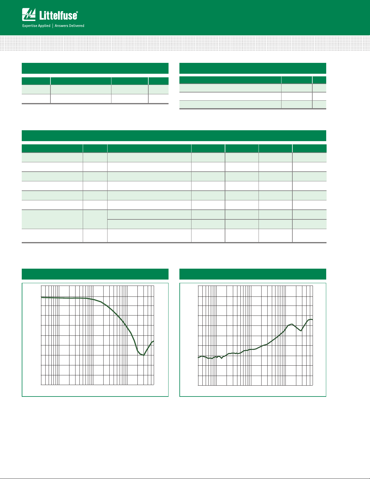
Analog Crosstalk (S41)Insertion Loss (S21)
0
-5
-10
-15
-20
Attenuation (dB)
-25
-30
-35
-40
-45
-50
10 1001000
Frequency (MHz)
Attenuation (dB)
-105
-120
-135
0
-15
-30
-45
-60
-75
-90
10 1001000
Frequency (MHz)
SP6003 Series
2
Revision: November 29, 2012
Please refer to http://www.littelfuse.com for current information.
Specifications are subject to change without notice.
©2012 Littelfuse, Inc.
 Loading...