

Page 1
TVS Diode Arrays (SPA
™
Family of Products)
ESD and EMI Filter Devices - SP6001 Series
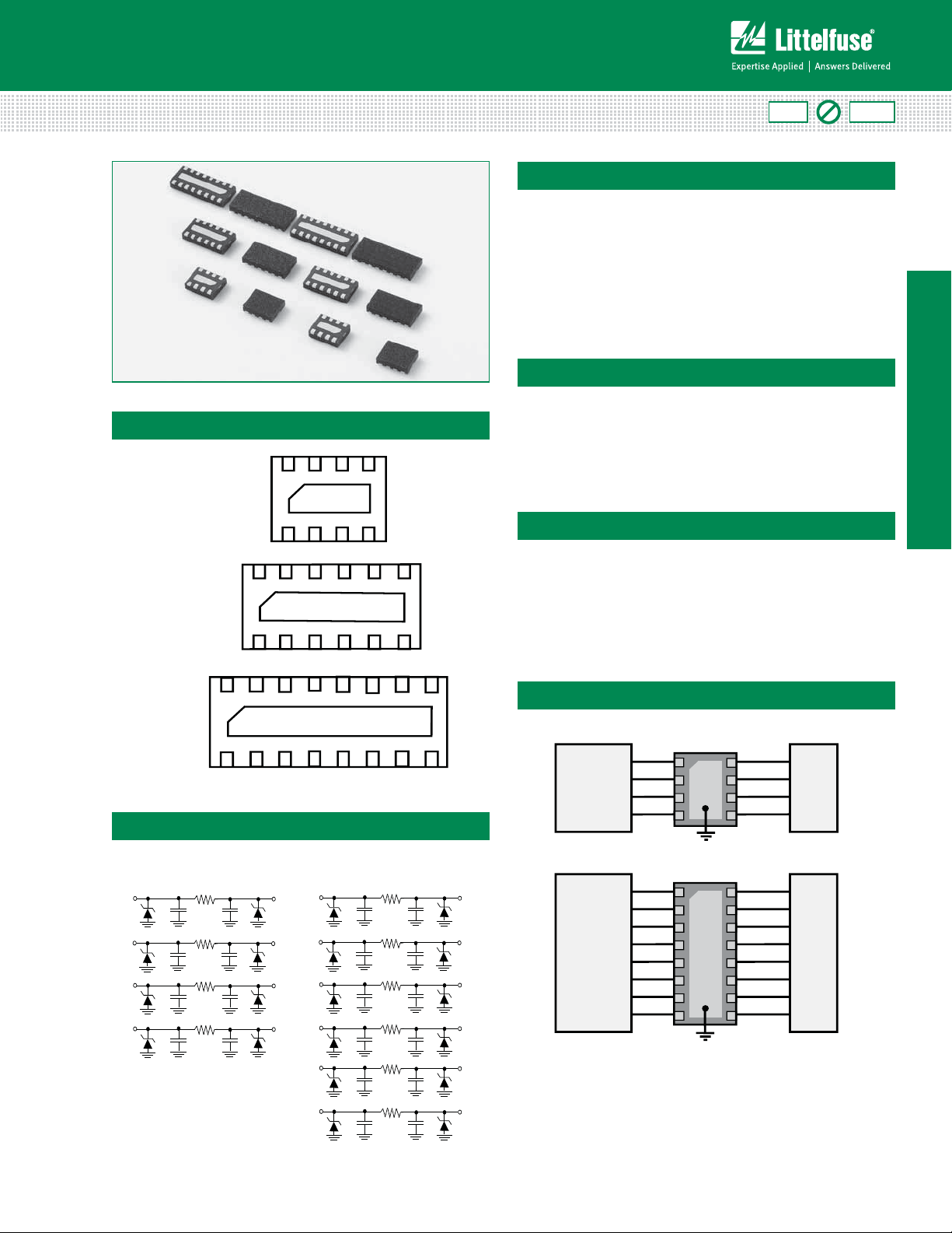
SP6001 Series 12pF 30kV EMI Filter Array
Pinout
μDFN-08
μDFN-12
1
12
1
8
SP6001-04UTG-1
SP6001-06UTG-1
GND
GND
4
5
6
7
RoHS
Pb
GREEN
Description
The Littelfuse SP6001 SPA series integrates 4, 6 and 8
EMI filters (C-R-C) into a small, low-profile DFN package
with each filter providing greater than -30dB attenuation at
1GHz. Additionally, each I/O is capable of shunting ±30kV
ESD strikes (IEC61000-4-2, contact discharge) away from
sensitive electronic components. The performance of this
small, slim design makes it extremely suitable for mobile
handsets, PDAs and notebook computers.
Features
t&.*mMUFSJOHPG
frequencies from
800MHz to 3GHz
t(SFBUFSUIBOE#
attenuation (TYP) at 1GHz
t&4%*&$
±30kV contact, ±30kV air
t4NBMMMPXQSPmMFç%'/
(JEDEC MO-229) package
(TYP 0.5mm height)
Applications
t,FZQBEJOUFSGBDFGPS
portable electronics
t-$%BOEDBNFSBEJTQMBZ
interfaces for handsets
t.PCJMFQIPOF
t4NBSUQIPOF
t1PSUBCMFOBWJHBUJPO
device
t$POOFDUPSJOUFSGBDFTGPS
portable electronics
SP6001
18
μDFN-16
16
GND
9
SP6001-08UTG-1
Functional Block Diagram
SP6001-04UTG-1
18
27
36
4 5
Cd Cd
Cd Cd
Cd Cd
Cd Cd
SP6001-06UTG-1
1
2
3
4
5
Cd Cd
Cd Cd
Cd Cd
Cd Cd
Cd Cd
67
Cd Cd
12
11
10
9
8
Application Examples
PCB Connector
for LCD Display
D1
D2
D3
D4
Camera Module
D1
D2
D3
D4
D5
D6
D7
D8
SP6001-08UTG-1
SP6001-04UTG-1
Baseband
IC
Baseband
IC
©2012 Littelfuse, Inc.
Specifications are subject to change without notice.
Please refer to www.littelfuse.com/SPA for current information.
169
Revision: March 20, 2012
SP6001 Series
Page 2
TVS Diode Arrays (SPA
™
Family of Products)
ESD and EMI Filter Devices - SP6001 Series
Absolute Maximum Ratings
Symbol Parameter Value Units
T
OP
T
STOR
CAUTION: Stresses above those listed in “Absolute Maximum Ratings” may cause
permanent damage to the device. This is a stress only rating and operation of the device
at these or any other conditions above those indicated in the operational sections of this
specification is not implied.
Electrical Characteristics (T
Reverse Standoff Voltage V
Breakdown Voltage V
Reverse Leakage Current I
Resistance R
Diode Capacitance
Line Capacitance
ESD Withstand Voltage
Cutoff Frequency
Notes: 1 Parameter is guaranteed by design and/or device characterization.
2
Total line capacitance is two times the diode capacitance (CD).
3
50 source and 50 load termination
Operating Temperature -40 to 85 °C
Storage Temperature -60 to 150 °C
=25ºC)
OP
Parameter Symbol Test Conditions Min Typ Max Units
RWM
BR
LEAK
A
1,2
1,2
1
3
C
D
C
L
V
F
IEC61000-4-2 (Contact Discharge) ±30 kV
ESD
-3dB
IEC61000-4-2 (Air Discharge) ±30 kV
Above this frequency, appreciable
IR=1mA 7.0 (90%TYP) 7.8 8.5 (109%TYP) V
V
=5V 0.1 1.0 µA
RWM
IR=10mA 85 (85%TYP) 100 115 (115% TYP)
VR=2.5V,f=1MHz 12 pF
VR=2.5V,f=1MHz 19 (79.2%TYP) 24 29 (120.8%TYP) pF
attenutation occurs
Thermal Information
Parameter Rating Units
Storage Temperature Range -65 to 150 °C
Maximum Junction Temperature 150 °C
Maximum Lead Temperature
(Soldering 20-40s)
6.0 V
115 MHz
260 °C
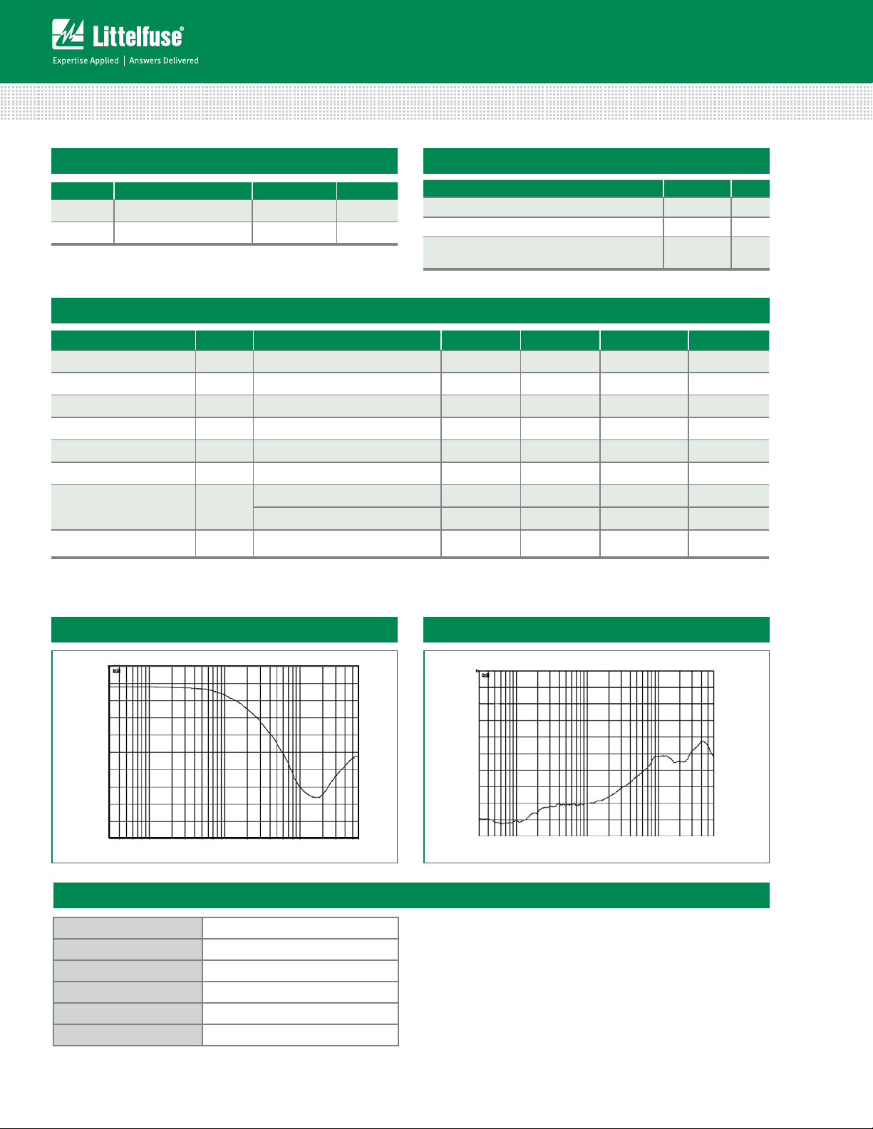
21 log MAG 5 dB/ REF 0 dB 1 _:-5.8807 dB
CH1 S
Cor
Smo
1
x2
Start
3.000 00 0MHz
Stop 6 000.00 0.000MHz
Product Characteristics
Lead Plating Pre-Plated Frame
Lead Material Copper Alloy
Lead Coplanarity 0.0004 inches (0.102mm)
Substitute Material Silicon
Body Material Molded Epoxy
Flammability UL 94 V-0
Analog Crosstalk (S41)Insertion Loss (S21)
CH1 S
Cor
Del
Smo
x2
START
Notes :
1. All dimensions are in millimeters
2. Dimensions include solder plating.
3. Dimensions are exclusive of mold flash & metal burr.
4. Blo is facing up for mold and facing down for trim/form, i.e. reverse trim/form.
5. Package surface matte finish VDI 11-13.
log MAG 10 dB/
1
3.000 000 MHz
REF 0 dB
Stop 6 000.000 0 00 MHz
SP6001 Series
170
Revision: March 20, 2012
Specifications are subject to change without notice.
Please refer to www.littelfuse.com/SPA for current information.
©2012 Littelfuse, Inc.
Page 3

TVS Diode Arrays (SPA
t
R
R
o
C
T
T
™
Family of Products)
ESD and EMI Filter Devices - SP6001 Series
Line Capacitance vs. DC Bias
50
40
30
20
Capacitance (pF)
10
0
0.0 0.5 1.0 1.5 2.0 2.5 3.0 3.5 4.0 4.5 5.0
DC Bias (V)
Package Dimensions — μDFN-08
D
Millimeters Inches
Min Max Min Max
A 0.450 0.550 0.018 0.022
A1 0.000 0.050 0.000 0.002
A3 0.127 REF 0.005 REF
b 0.150 0.250 0.006 0.010
D 1.600 1.800 0.063 0.071
D2 1.100 1.300 0.043 0.051
E 1.250 1.450 0.049 0.057
E2 0.300 0.500 0.012 0.020
e 0.400 BSC 0.016 BSC
K 0.200 0.008 0.000
L 0.150 0.350 0.006 0.014
A3
E
A
D2
A1
E2
K
L
e
b
μDFN-08
JEDEC MO-229
Soldering Parameters
Reflow Condition Pb – Free assembly
- Temperature Min (T
Pre Heat
- Temperature Max (T
- Time (min to max) (ts) 60 – 180 secs
Average ramp up rate (Liquidus) Temp
(T
) to peak
L
to TL - Ramp-up Rate 3°C/second max
T
S(max)
Reflow
- Temperature (TL) (Liquidus) 217°C
- Temperature (tL) 60 – 150 seconds
Peak Temperature (TP) 260
Time within 5°C of actual peak
Temperature (t
)
p
Ramp-down Rate 6°C/second max
Time 25°C to peak Temperature (T
Do not exceed 260°C
T
P
T
L
T
S(max)
t
PreheatPrehea
S
Temperature
T
S(min)
25
time to peak temperature
) 150°C
s(min)
) 200°C
s(max)
3°C/second max
20 – 40 seconds
) 8 minutes Max.
P
t
P
Ramp-up
amp-up
t
+0/-5
L
Ramp-down
amp-d
Time
°C
Critical Zone
ritical Zone
T
L to TP
to
SP6001
Package Dimensions — μDFN-16
μDFN-16
JEDEC MO-229
D
E
A
A3
D2
K
e
©2012 Littelfuse, Inc.
Specifications are subject to change without notice.
Please refer to www.littelfuse.com/SPA for current information.
b
A1
E2
L
Millimeters Inches
Min Max Min Max
A 0.45 0.55 0.01 0.02
A1 0.00 0.05 0.00 0.002
A3 0.127 REF 0.00 REF
b 0.15 0.25 0.00 0.00
D 3.20 3.40 0.12 0.13
D2 2.70 2.90 0.10 0.11
E 1.25 1.45 0.04 0.05
E2 0.30 0.50 0.01 0.01
e 0.40 BSC 0.01 BSC
K 0.20 0.00
L 0.15 0.35 0.00 0.01
Revision: March 20, 2012
Package Dimensions — μDFN-12
D
E
A
A1
E2
L
b
171
A3
K
D2
e
μDFN-12
JEDEC MO-229
Millimeters Inches
Min Max Min Max
A 0.450 0.550 0.018 0.022
A1 0.000 0.050 0.000 0.002
A3 0.127 REF 0.005 REF
b 0.150 0.250 0.006 0.010
D 2.400 2.600 0.094 0.102
D2 1.900 2.100 0.075 0.083
E 1.250 1.450 0.049 0.057
E2 0.300 0.500 0.012 0.020
e 0.400 BSC 0.016 BSC
K 0.200 0.008 0.000
L 0.150 0.350 0.006 0.014
SP6001 Series
Page 4

TVS Diode Arrays (SPA
™
Family of Products)
ESD and EMI Filter Devices - SP6001 Series
Embossed Carrier Tape & Reel Specification – μDFN-08
P2
D
EF
t
AO
W
D1
P
BO
KO
Millimetres Inches
Min Max Min Max
E 1.65 1.85 0.065 0.073
F 3.45 3.55 0.136 0.140
D1 1.00 - 0.040 -
D 1.50 min 0.059 min
P 3.90 4.10 0.154 0.161
10P 40.0 +/- 0.20 1.575 +/- 0.008
W 7.70 8.30 0.303 0.327
P2 1.95 2.05 0.077 0.081
A0 1.55 1.75 0.061 0.069
1.90 2.1 0.075 0.083
B0
K0 0.95 1.15 0.037 0.045
t 0.30 max 0.012 max
Embossed Carrier Tape & Reel Specification – μDFN-12
P2
oD
/
oD
/
E
W
BO
F
t
A0
K0
P
Millimetres Inches
Min Max Min Max
E 1.65 1.85 0.065 0.073
F 3.45 3.55 0.136 0.140
D1 0.55 0.65 0.021 0.025
D 1.50 min 0.059 min
P 3.90 4.10 0.154 0.161
10P 40.0 +/- 0.20 1.575 +/- 0.008
W 7.90 8.30 0.311 0.327
P2 1.95 2.05 0.077 0.081
A0 1.33 1.53 0.052 0.060
B0
2.63 2.83 0.103 0.111
K0 0.58 0.78 0.023 0.031
t 0.22 max 0.009 max
Embossed Carrier Tape & Reel Specification – μDFN-16
P2
SP6001 Series
P0
++ +
W
++
12º MAX
A0
+
T
K0
Min Max Min Max
A0 1.55 1.75 0.06 0.06
B0 3.50 3.70 0.13 0.14
D0 1.40 1.60 0.05 0.06
E 1.65 1.85 0.06 0.07
F 5.45 5.55 0.21 0.21
K0 0.85 1.05 0.03 0.04
P0 3.90 4.10 0.15 0.16
P1 1.95 2.05 0.07 0.08
P2 3.90 4.10 0.15 0.16
0.26 0.30 0.01 0.01
T
W 11.90 12.30 0.46 0.48
D0
P1
E
++
F
+
+
1.00 ± 0.05
Ø
B0
12º MAX
Millimetres Inches
Part Numbering System
Silicon Protection Array (SPATM)
Family of TVS Diode Arrays
Part Marking System
Ordering Information
Part Number Package Size
SP6001-04UTG-1 DFN-08 1.7x1.35 J*4 3000
SP6001-06UTG-1 DFN-12 2.5x1.35 J
SP6001-08UTG-1 DFN-16 3.3x1.35 J
172
Revision: March 20, 2012
SP 6001 ** U T
Series
Number of Channels
04 = 4 Channel μDFN-08
06 = 6 Channel μDFN-12
08 = 8 Channel μDFN-16
Product Series
J = SP6001
Please refer to www.littelfuse.com/SPA for current information.
G -1
G= Green
T= Tape & Reel
Package
μDFN-08 (1.7x1.35mm)
μDFN-12 (2.5x1.35mm)
μDFN-16 (3.3x1.35mm)
J * *
4 = μDFN-08
6 = μDFN-12
Assembly Site
(mm)
Specifications are subject to change without notice.
8 = μDFN-16
Marking Min. Order
*6 3000
*8 3000
©2012 Littelfuse, Inc.
Qty.
 Loading...