

Page 1
TVS Diode Arrays (SPA
I/O 8
I/O 7
I/O 6
I/O 5
I/O 1
I/O 2
GND
I/O 3
I/O 4
I/O 1
I/O 2
GND
I/O 3
I/O 4
NC
I/O 8
I/O 7
I/O 6
I/O 5
RoHS
GREEN
LVDS Controller
Outside
World
CLK+
Shield GND
CLK-
A0+
A0-
A1+
A1-
A2+
A2-
Signal
Shield GND
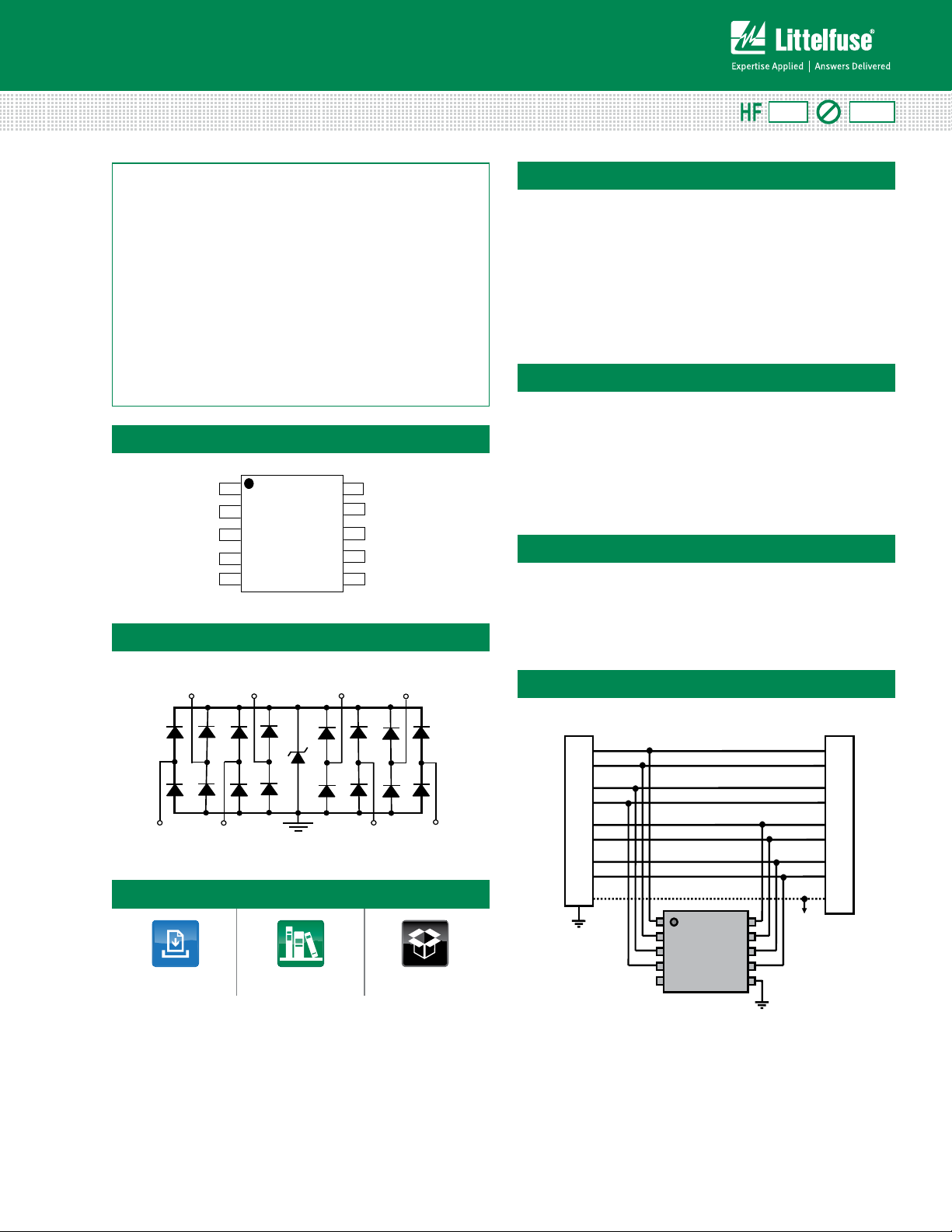
SP4060-08ATG
LVDS Interface
®
Diodes)
Lightning Surge Protection - SP4060 Series
SP4060 Series 2.5V 20A Diode Array
Pinout
Pb
Description
The SP4060 integrates low capacitance diodes with an
additional zener diode to protect each I/O pin against
ESD and high surge events. This robust device can safely
absorb up to 20A per IEC61000-4-5 (t
performance degradation and a minimum ±30kV ESD per
IEC61000-4-2 International Standard. Their low loading
capacitance also makes them ideal for protecting high
speed signal pins.
Features
• ESD, IEC61000-4-2,
±30kV contact, ±30kV air
• EFT, IEC61000-4-4, 40A
(5/50ns)
• Lightning, IEC61000-4-5,
20A (8/20µs)
Applications
=8/20µs) without
p
• Low capacitance of 4.4pF
(TYP) per I/O
• Low leakage current of
1µA (MAX) at 2.5V
Functional Block Diagram
Additional Information
Datasheet
Resources
Samples
• LCD/PD TVs
• Desktops
• Game Consoles
Application Example
• Set Top Boxes
• Notebooks
Life Support Note:
Not Intended for Use in Life Support or Life Saving Applications
The products shown herein are not designed for use in life sustaining or life saving
applications unless otherwise expressly indicated.
© 2013 Littelfuse, Inc.
Specifications are subject to change without notice.
Revised: 04/24/13
Page 2
TVS Diode Arrays (SPA
0%
10%
20%
30%
40%
50%
60%
70%
80%
90%
100%
110%
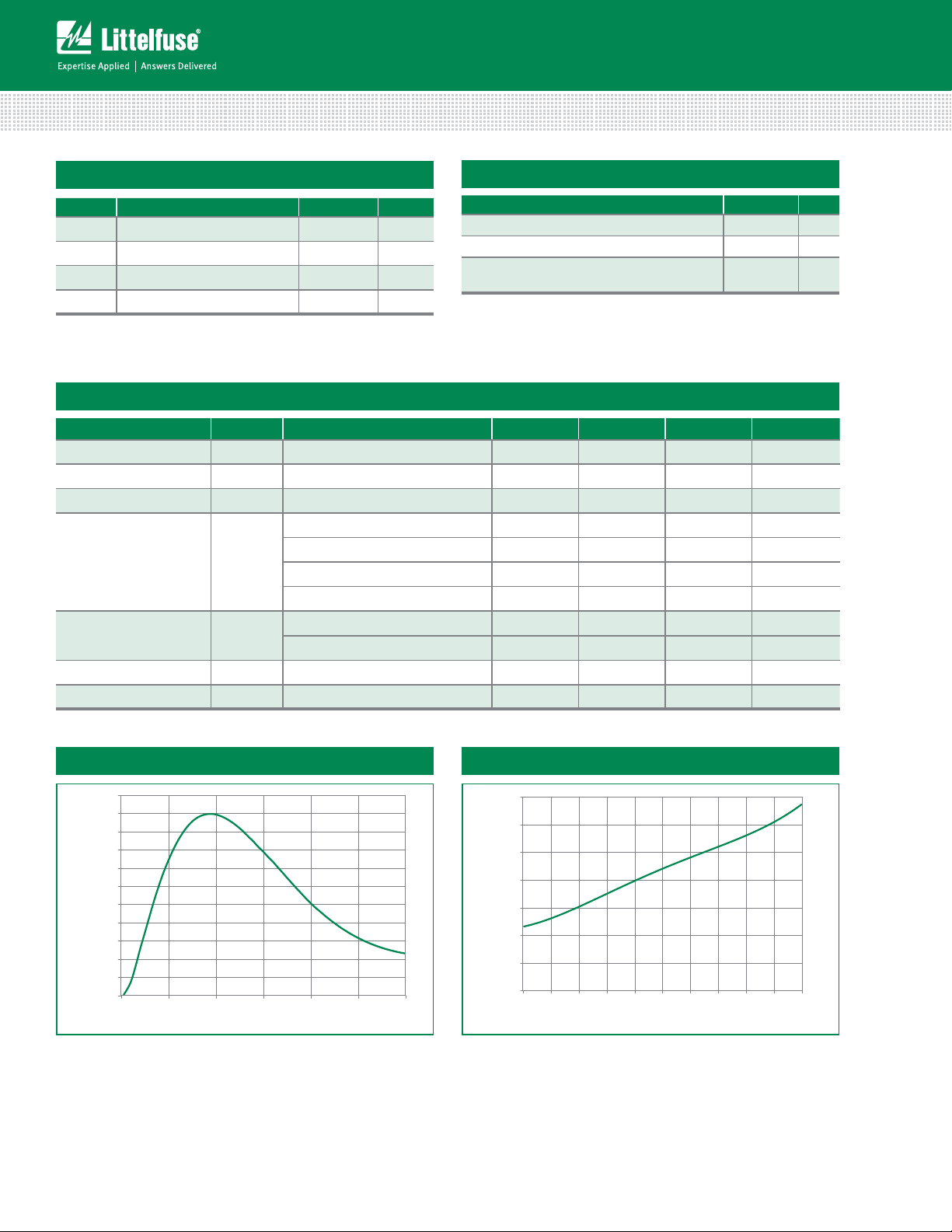
0.0 5.0 10.0 15.0 20.0 25.0 30.0
Time (μs)
Percent of I
PP
0.0
2.0
4.0
6.0
8.0
10.0
12.0
14.0
Peak Pulse Current-I
PP
(A)
Clamp Voltage (V
C
)
1.0 3.0 5.0 7.0 9.0 11.0 13.0 15.0 17.0 19.0 21.0
®
Diodes)
Lightning Surge Protection - SP4060 Series
Absolute Maximum Ratings
Symbol Parameter Value Units
I
PP
P
PK
T
OP
T
STOR
CAUTION: Stresses above those listed in “Absolute Maximum Ratings” may cause
permanent damage to the device. This is a stress only rating and operation of the device
at these or any other conditions above those indicated in the operational sections of this
specification is not implied.
Electrical Characteristics (T
Reverse Standoff Voltage V
Snap Back Voltage V
Reverse Leakage Current I
Clamp Voltage
ESD Withstand Voltage
Diode Capacitance
Diode Capacitance
Note: 1. Parameter is guaranteed by design and/or device characterization.
Peak Current (tp=8/20μs) 20.0 A
Peak Pulse Power (tp=8/20µs) 300 W
Operating Temperature –40 to 125 ºC
Storage Temperature –55 to 150 °C
=25ºC)
OP
Parameter Symbol Test Conditions Min Typ Max Units
RWM
SB
LEAK
ISB=50mA 2.0 V
VR=2.5V, I/O to GND 0.5 1. 0 µA
IPP=1A, tp=8/20µs, Fwd 4.5 5.5 V
I
=5A, tp=8/20µs, Fwd 6.0 7. 2 V
1
1
1
1
V
C
I/O-GND
C
V
C
ESD
I/O-I/O
PP
I
=10A, tp=8/20µs, Fwd 8.0 9.6 V
PP
I
=20A, tp=8/20µs, Fwd 12.5 15.0 V
PP
IEC61000-4-2 (Contact) ±30 kV
IEC61000-4-2 (Air) ±30 kV
Reverse Bias=0V 4.4 5.0 pF
Reverse Bias=0V 2.2 pF
Thermal Information
Parameter Rating Units
Storage Temperature Range –55 to 150 °C
Maximum Junction Temperature 150 °C
Maximum Lead Temperature
(Soldering 20-40s)
2.5 V
260 °C
Pulse Waveform
Clamping Voltage vs. I
PP
Specifications are subject to change without notice.
© 2013 Littelfuse, Inc.
Revised: 04/24/13
Page 3

TVS Diode Arrays (SPA
0.0
1.0
2.0
3.0
4.0
5.0
0.0 0.5 1.0 1.5 2.0 2.5
DC Bias (V)
Capacitance (pF)
-30
-25
-20
-15
-10
-5
0
5
00001000100101
Frequency (MHz)
Attenuation (dB)
t
R
R
o
C
e
T
L
T
P
B
e
A1
A
21
E1
E
10
D
L
C
0.32
[0.0126]
4.24
[0.1669]
1.04
[0.0409]
5.28
[0.2079]
3.20
[0.1260]
0.50
[0.0197]
2.00
[0.0787]
Solder Pad Layout
®
Diodes)
Lightning Surge Protection - SP4060 Series
Capacitance vs. Bias Insertion Loss (S21) I/O to GND
Soldering Parameters
Reflow Condition Pb – Free assembly
- Temperature Min (T
Pre Heat
- Temperature Max (T
- Time (min to max) (ts) 60 – 180 secs
Average ramp up rate (Liquidus) Temp
(T
) to peak
L
to TL - Ramp-up Rate 3°C/second max
T
S(max)
Reflow
- Temperature (TL) (Liquidus) 217°C
- Temperature (tL) 60 – 150 seconds
Peak Temperature (TP) 260
Time within 5°C of actual peak
Temperature (t
)
p
Ramp-down Rate 6°C/second max
Time 25°C to peak Temperature (T
Do not exceed 260°C
Package Dimensions — MSOP10
© 2013 Littelfuse, Inc.
Specifications are subject to change without notice.
Revised: 04/24/13
t
P
t
L
Critical Zone
ritical Zon
L to TP
to
T
Ramp-down
amp-d
Time
) 150°C
s(min)
) 200°C
s(max)
3°C/second max
+0/-5
°C
T
P
Ramp-up
t
amp-up
PreheatPrehea
S
T
L
T
S(max)
Temperature
T
S(min)
25
time to peak temperature
20 – 40 seconds
) 8 minutes Max.
P
Package
Pins 10
JEDEC MO-187
Millimeters Inches
DIM
Min Max Min Max
A - 1. 10 - 0.043
A1 0.00 0.15 0.000 0.006
B 0.17 0.27 0.007 0.011
c 0.08 0.23 0.003 0.009
D 2.90 3.10 0.114 0.122
E 4.67 5.10 0.184 0.200
E1 2.90 3.10 0.114 0.122
e 0.50 BSC 0.020 BSC
L 0.40 0.80 0.016 0.032
MSOP
Page 4

TVS Diode Arrays (SPA
SP
4060 08
A T
G
Series
Number of
Channels
Package
A = MSOP10
T= Tape & Reel
G= Green
-
TVS Diode Arrays
(SPA
®
Diodes)
YYWW = Date code
F
L
YYWWD
P*8
Product Series
P = SP4060
Number of
Channels
Assembly Site
®
Diodes)
Lightning Surge Protection - SP4060 Series
Part Numbering System
Part Marking System
Ordering Information
Part Number Package Marking Min. Order Qty.
SP4060-08ATG MSOP10 P*8 4000
Product Characteristics
Lead Plating Pre-Plated Frame
Lead Material Copper Alloy
Lead Coplanarity 0.0004 inches (0.102mm)
Substitute Material Silicon
Body Material Molded Epoxy
Flammability UL 94 V-0
Notes :
1. All dimensions are in millimeters
2. Dimensions include solder plating.
3. Dimensions are exclusive of mold flash & metal burr.
4. Blo is facing up for mold and facing down for trim/form, i.e. reverse trim/form.
5. Package surface matte finish VDI 11-13.
Embossed Carrier Tape & Reel Specification — MSOP-10
Pin 1 Location
User Feeding Direction
Millimetres Inches
Min Max Min Max
E 1.65 1.85 0.065 0.073
F 5.40 5.60 0.213 0.220
D 1.50 1.60 0.059 0.063
D1 1.50 Min 0.059 Min
P0 3.90 4.10 0.154 0.161
10P0 40.0± 0.20 1.574±0.008
W 11.90 12.10 0.469 0.476
P 7.90 8.10 0.311 0.319
A0 5.20 5.40 0.205 0.213
B0 3.20 3.40 0.126 0.134
K0 1.20 1.40 0.047 0.055
t 0.30 ± 0.05 0.012± 0.002
Specifications are subject to change without notice.
© 2013 Littelfuse, Inc.
Revised: 04/24/13
 Loading...