

Page 1
TVS Diode Arrays (SPA
1
2
1
2
1
2
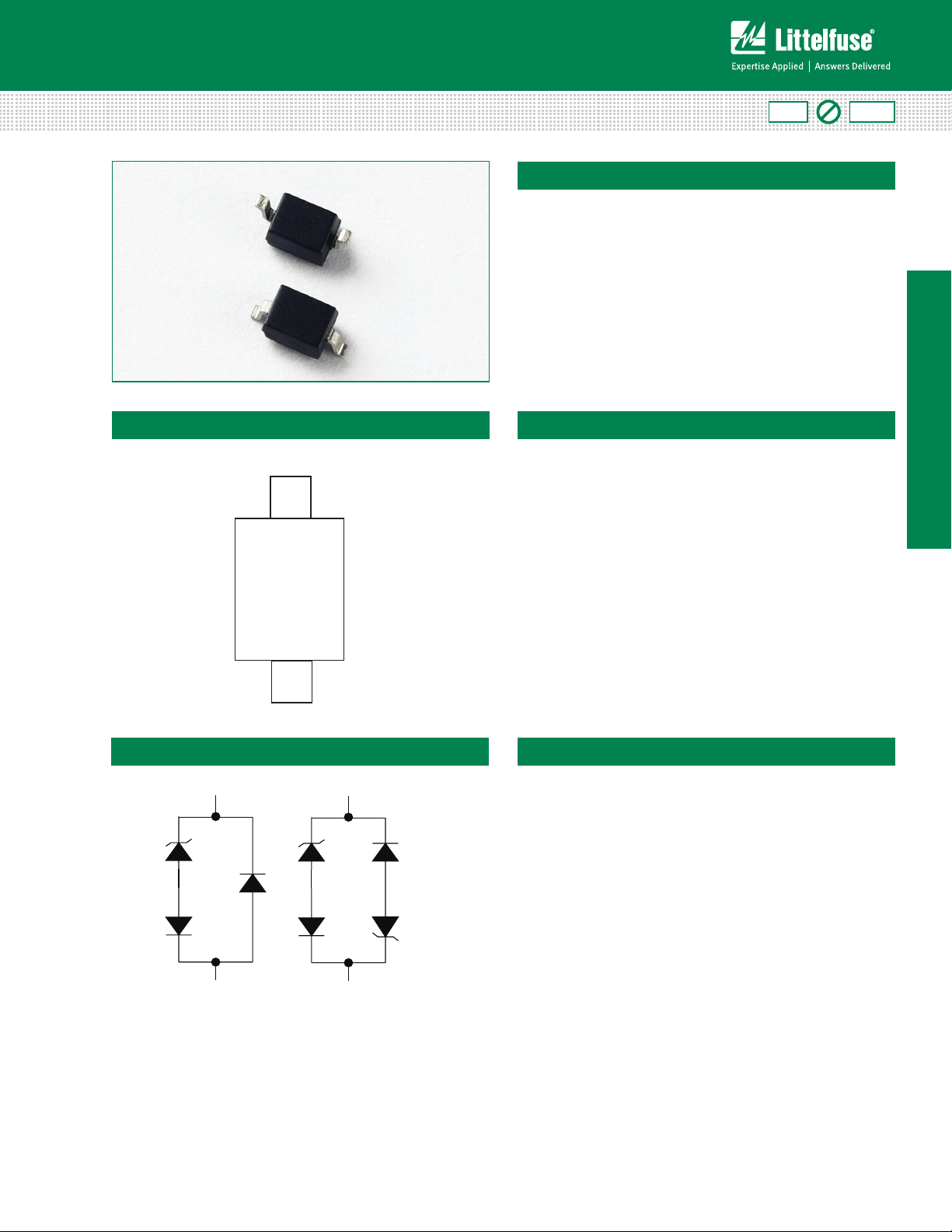
Unidirectional Bidirectional
SP4021-01FTG SP4021-01FTG-C
®
Diodes)
Lightning Surge Protection- SP4021 Series
SP4021 Series 2.5pF, 25A Discrete TVS Diode
Description
The SP4021 devices integrate low capacitance steering
diodes with one or two zener diodes for unidirectional or
bidirectional protection, respectively, to protect against
ESD and lightning induced surge events. These devices
can safely absorb up to 25A per IEC61000-4-5 (tp=8/20μs)
without performance degradation and a minimum ±30kV
ESD per IEC61000-4-2 International Standard. The low
loading capacitance and high surge capability make it ideal
for protecting telecommunication ports such as Ethernet
and other high speed data interfaces.
Pinout
Features
• ESD, IEC61000-4-2,
±30kV contact, ±30kV air
• EFT, IEC61000-4-4, 40A
(5/50ns)
• Lightning, IEC61000-4-5,
25A (t
• Low capacitance of 2.5pF
(@ V
=8/20μs)
P
=0V)
R
RoHS
Pb
GREEN
• Low leakage current
• Unidirectional and
Bidirectional configuration
• Small SOD323 package
fits 0805 footprints
SP4021
Functional Block Diagram
Life Support Note:
Not Intended for Use in Life Support or Life Saving Applications
The products shown herein are not designed for use in life sustaining or life saving
applications unless otherwise expressly indicated.
©2013 Littelfuse, Inc.
Specifications are subject to change without notice.
Please refer to www.littelfuse.com for current information.
Applications
•10/100/1000 Ethernet
•T1/E1/T3/E3
•USB 1.1/2.0
•Power Ports
1
Revision: July 12, 2013
•Computers and Peripherals
•Instrumentation
•Medical Equipment
SP4021 Series
Page 2
TVS Diode Arrays (SPA
01
®
Diodes)
Lightning Surge Protection- SP4021 Series
Absolute Maximum Ratings
Symbol Parameter Value Units
I
PP
P
Pk
T
OP
T
STOR
Notes:
CAUTION: Stresses above those listed in “Absolute Maximum Ratings” may cause permanent damage to the device. This is a stress only rating and operation of
the device at these or any other conditions above those indicated in the operational sections of this specification is not implied.
Thermal Information
Storage Temperature Range -55 to 150 °C
Maximum Junction Temperature 150 °C
Maximum Lead Temperature (Soldering 20-40s) 260 °C
Peak Current (tp=8/20μs) 25 A
Peak Pulse Power (tp=8/20μs)
600
W
Operating Temperature -40 to 125 °C
Storage Temperature -55 to 150 °C
Parameter Rating Units
Electrical Characteristics (T
OP
=25ºC)
Parameter Symbol Test Conditions Min Typ Max Units
Breakdown Voltage V
Reverse Standoff Voltage V
Leakage Current I
BD
RWM
LEAK
IR=2uA 6.3 V
IR≤1μA 5.0 V
VR=5.0V 0.5 μA
IPP=1A, tp=8/20µs, Fwd 9.3 V
Clamp Voltage
Dynamic Resistance R
ESD Withstand Voltage
Diode Capacitance
Note:
1
Parameter is guaranteed by design and/or device characterization.
Normalized Capacitance vs. Bias Voltage
3.5
3.0
2.5
2.0
1.5
1.0
Normalized Capacitance (pF)
0.5
0.0
1
1
1
SP4021-01FTG SP4021-01FTG-C
0.0 0.5 1.0 1.5 2.0 2.5 3.0 3.5 4.0 4.5 5.0
V
C
DYN
V
ESD
C
D
Bias Voltage (V)
I
=10A, tp=8/20µs, Fwd 14.0 V
PP
I
=24A, tP=8/20μs, Fwd 19.6 V
PP
(VC2 - VC1) / (I
PP2
- I
IEC61000-4-2 (Contact Discharge) ±30 kV
IEC61000-4-2 (Air Discharge) ±30 kV
Reverse Bias=0V, f=1MHz 2.5 pF
) 0.52 Ω
PP1
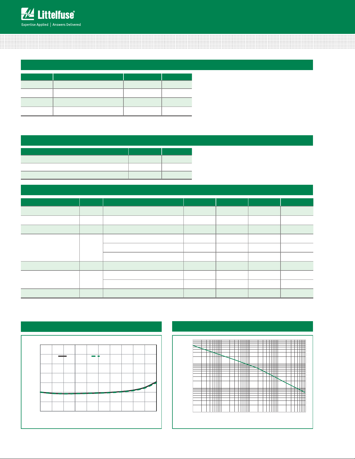
Non-Repetitive Peak Pulse Power vs. Pulse Time
10
(kW)
pk
1
0.1
Peak Pulse Power - P
0.01
0.11 10 10
Pulse Duration - t
p
(µs)
000
2
Revision: July 12, 2013
Please refer to http://www.littelfuse.com for current information.
Specifications are subject to change without notice.
©2013 Littelfuse, Inc.
Page 3

TVS Diode Arrays (SPA
25.0
10.0
20.0
5.0
15.0
Clamp Voltage (V
C
)
0.0
4.0
8.0
12.0
16.0
20.0
24.0
1.
0
Peak Pulse Current-I
PP
(A)
t
R
R
o
C
e
T
L
T
P
0%
10%
20%
30%
40%
50%
60%
70%
80%
90%
100%
110%
0.0 5.0 10.0 15.0 20.0 25.0 30.0
Time (μs)
Percent of I
PP
®
Diodes)
Lightning Surge Protection- SP4021 Series
Clamping Voltage vs. I
PP
Soldering Parameters
Reflow Condition Pb – Free assembly
- Temperature Min (T
Pre Heat
- Temperature Max (T
- Time (min to max) (ts) 60 – 180 secs
Average ramp up rate (Liquidus) Temp
(T
) to peak
L
to TL - Ramp-up Rate 3°C/second max
T
S(max)
Reflow
- Temperature (TL) (Liquidus) 217°C
- Temperature (tL) 60 – 150 seconds
Peak Temperature (TP) 260
Time within 5°C of actual peak
Temperature (t
)
p
Ramp-down Rate 6°C/second max
Time 25°C to peak Temperature (T
Do not exceed 260°C
) 150°C
s(min)
) 200°C
s(max)
3°C/second max
+0/-5
°C
20 – 40 seconds
) 8 minutes Max.
P
Pulse Waveform
T
P
T
L
T
S(max)
Temperature
T
S(min)
25
time to peak temperature
t
S
PreheatPrehea
Ramp-up
amp-up
t
P
t
L
Critical Zone
ritical Zon
T
L to TP
to
Ramp-down
amp-d
Time
SP4021
Product Characteristics
Lead Plating
Lead Material Copper Alloy
Lead Coplanarity 0.0004 inches (0.102mm)
Substitute Material Silicon
Body Material Molded Epoxy
Flammability UL 94 V-0
Notes :
1. All dimensions are in millimeters
2. Dimensions include solder plating.
3. Dimensions are exclusive of mold flash & metal burr.
4. Blo is facing up for mold and facing down for trim/form, i.e. reverse trim/form.
5. Package surface matte finish VDI 11-13.
©2013 Littelfuse, Inc.
Specifications are subject to change without notice.
Please refer to www.littelfuse.com for current information.
Matte Tin
3
Revision: July 12, 2013
SP4021 Series
Page 4

TVS Diode Arrays (SPA
4.00
2.00
®
Diodes)
Lightning Surge Protection- SP4021 Series
Part Marking System
SP4021-01FTG
05
SP4021-01FTG-C
5C
Package Dimensions -SOD323
E
b
E1
L
0.2
L1
L
c
A1
A2
A
Part Numbering System
TVS Diode Arrays
®
(SPA
Diodes )
Series
Number of
Channels
Ordering Information
Part Number Package Marking Min. Order Qty.
SP4021-01FTG SOD323 05 3000
SP4021-01FTG-C SOD323 5C 3000
Symbol
A 1. 0 0 0.039
D
A1 0.00 0.10 0.000 0.004
A2 0.80 0.90 0.031 0.035
b 0.25 0.35 0. 010 0.014
c 0.08 0.15 0.003 0.006
D 1.20 1.40 0.047 0.055
E 1.60 1.80 0.063 0.071
E1 2.50 2.70 0.098 0.106
L 0.475 REF 0.019 REF
L1 0.25 0.40 0. 010 0.016
Ø 0º 8º 0º 8º
–
4021
SP
01
T
F
G
C
G= Green
T= Tape & Reel
Package
F: SOD323
Blank= Unidirectional
C= Bidirectional
SOD323
Millimeters Inches
Min Max Min Max
Embossed Carrier Tape & Reel Specification — SOD323
ø1.50
1.75
2.90
1.25
B-B
B
B
Cover Tape
3.50
8.00
Revision: July 12, 2013
4.00
1.46
A-A
A
A
0.254
R78.0
R25.6
4
R25.6
12.3
3000
2500
2000
1500
1000
500
R6.5
54.4
12.3
9.5
Please refer to http://www.littelfuse.com for current information.
Specifications are subject to change without notice.
ø178
©2013 Littelfuse, Inc.
 Loading...