

TVS Diode Arrays (SPA
RoHS
GREEN
1
2
1
2
1
2
Unidirectional Bidirectional
SP4020-01FTG SP4020-01FTG-C
®
Diodes)
Lightning Surge Protection- SP4020 Series
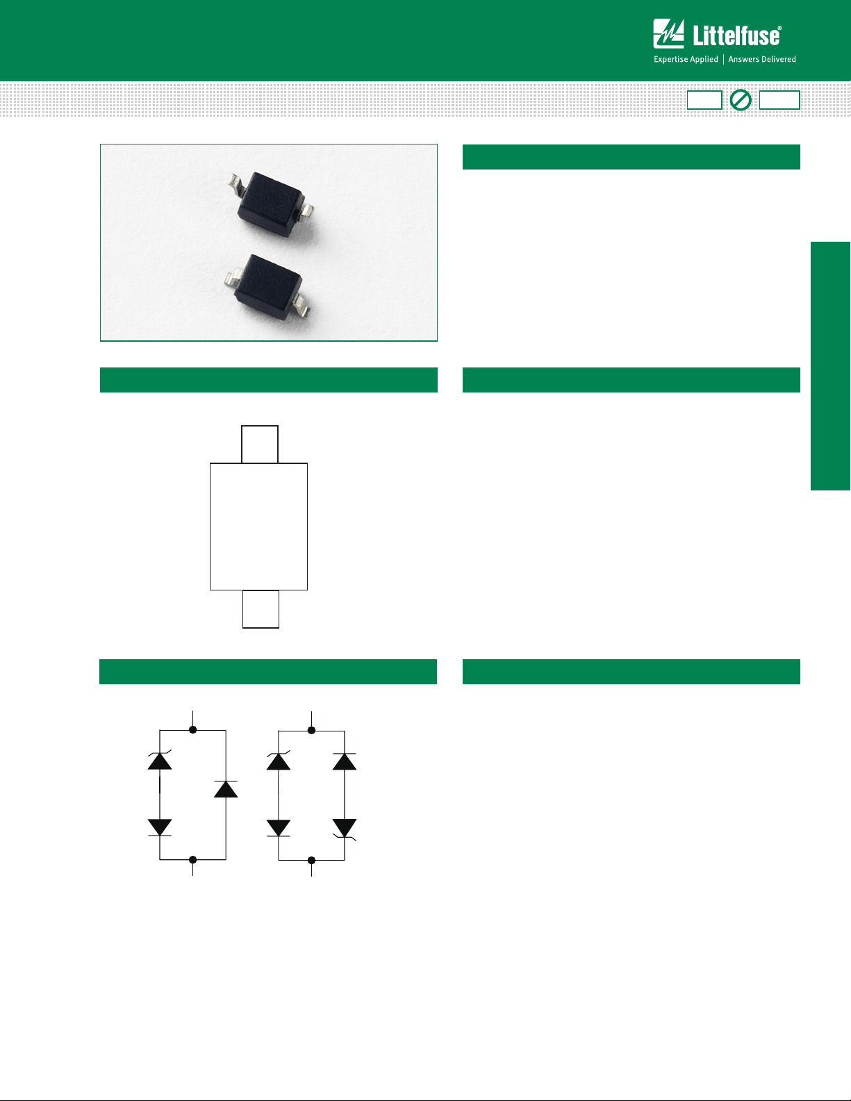
SP4020 Series 2.5pF, 30A Discrete TVS Diode
Description
The SP4020 devices integrate low capacitance steering
diodes with one or two zener diodes for unidirectional or
bidirectional protection, respectively, to protect against
ESD and lightning induced surge events. These devices
can safely absorb up to 30A per IEC61000-4-5 (tp=8/20μs)
without performance degradation and a minimum ±30kV
ESD per IEC61000-4-2 International Standard. The low
loading capacitance and high surge capability make it ideal
for protecting telecommunication ports such as Ethernet
and other high speed data interfaces.
Pinout
Features
• ESD, IEC61000-4-2,
±30kV contact, ±30kV air
• EFT, IEC61000-4-4, 40A
(5/50ns)
• Lightning, IEC61000-4-5,
30A (tP=8/20μs)
• Low capacitance of 2.5pF
(@ VR=0V)
• Low leakage current of
0.1μA at 3.3V
Pb
SP4020
• Unidirectional and
Bidirectional configuration
• Small SOD323 package
fits 0805 footprints
Functional Block Diagram
Life Support Note:
Not Intended for Use in Life Support or Life Saving Applications
The products shown herein are not designed for use in life sustaining or life saving
applications unless otherwise expressly indicated.
© 2013 Littelfuse, Inc.
Specifications are subject to change without notice.
Revised: September 22, 2013
Applications
•10/100/1000 Ethernet
•T1/E1/T3/E3
•USB 1.1/2.0
•Power Ports
•Computers and Peripherals
•Instrumentation
•Medical Equipment
SP4020 Series
TVS Diode Arrays (SPA
01
®
Diodes)
Lightning Surge Protection- SP4020 Series
Absolute Maximum Ratings
Symbol Parameter Value Units
I
PP
P
Pk
T
OP
T
STOR
Notes:
CAUTION: Stresses above those listed in “Absolute Maximum Ratings” may cause permanent damage to the device. This is a stress only rating and operation of
the device at these or any other conditions above those indicated in the operational sections of this specification is not implied.
Thermal Information
Storage Temperature Range -55 to 150 °C
Maximum Junction Temperature 150 °C
Maximum Lead Temperature (Soldering 20-40s) 260 °C
Peak Current (tp=8/20μs) 30 A
Peak Pulse Power (tp=8/20μs)
750
W
Operating Temperature -40 to 125 °C
Storage Temperature -55 to 150 °C
Parameter Rating Units
Electrical Characteristics (T
OP
=25ºC)
Parameter Symbol Test Conditions Min Typ Max Units
Breakdown Voltage V
Reverse Standoff Voltage V
Leakage Current I
BD
RWM
LEAK
IR=2uA 3.5 V
IR≤1μA 3.3 V
VR=3.3V 0.1 0.5 μA
IPP=1A, tp=8/20µs, Fwd 6.6 V
Clamp Voltage
1
V
C
IPP=10A, tp=8/20µs, Fwd 14.2 V
IPP=24A, tP=8/20μs, Fwd 21.8 V
Dynamic Resistance R
ESD Withstand Voltage
Diode Capacitance
Note:
1
Parameter is guaranteed by design and/or device characterization.
1
1
DYN
V
ESD
C
D
Normalized Capacitance vs. Bias Voltage
1.4
1.2
1.0
0.8
0.6
0.4
Normalized Capacitance (pF)
0.2
0.0
0.0 0.3 0.6 0.9 1.2 1.5 1.8 2.1 2.4 2.7 3.0 3.3
SP4020 Series
SP4020-01FTG-C SP4020-01FTG
Bias Voltage (V)
(VC2 - VC1) / (I
- I
) 0.7 Ω
PP2
PP1
IEC61000-4-2 (Contact Discharge) ±30 kV
IEC61000-4-2 (Air Discharge) ±30 kV
Reverse Bias=0V, f=1MHz 2.5 pF
Non-Repetitive Peak Pulse Power vs. Pulse Time
10
(kW)
pk
1
0.1
Peak Pulse Power - P
0.01
0.11 10 10
Pulse Duration - t
Specifications are subject to change without notice.
p
(µs)
000
© 2013 Littelfuse, Inc.
Revised: September 22, 2013
 Loading...