


TVS Diode Arrays (SPA
VCC
10/100
Ethernet
PHY
TX +
TX -
RX +
RX -
VCC
GND
SP3051-04HTG
TX +
TX -
RX +
RX -
Unused
Unused
Unused
RJ45
Unused
To Twisted-Pair Network
75
75
75
75
1
2
3
6
5
4
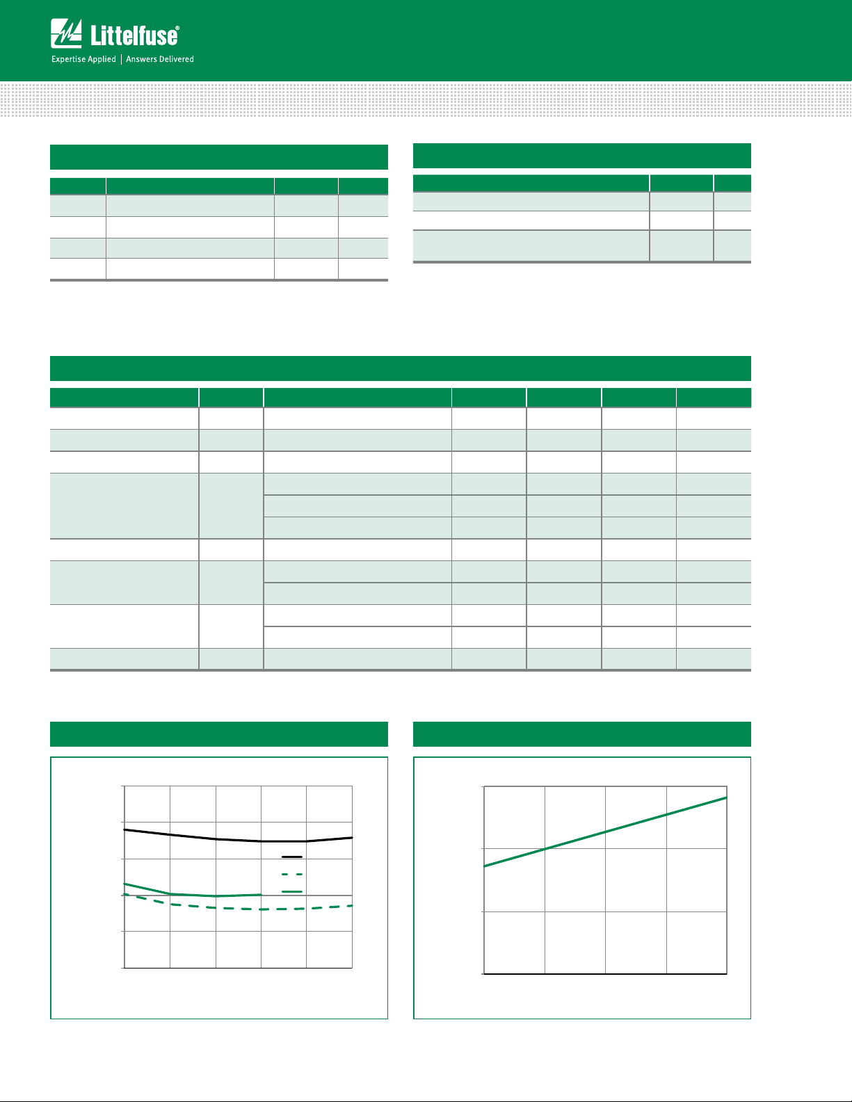
10/100 Ethernet Differential Protection
®
Diodes)
Lightning Surge Protection - SP3051 Series
SP3051 Series 6V 20A Diode Array
Pinout
I/O 1
GND
I/O 2
Functional Block Diagram
I/O 4
V
CC
I/O 3
RoHS
Pb
GREEN
Description
The SP3051 integrates low capacitance rail-to-rail diodes
with an additional zener diode to protect each I/O pin
against ESD and high surge events. This robust device can
safely absorb 20A of current per IEC61000-4-5 (t
=8/20µs)
P
without performance degradation and a minimum ±30kV
ESD per IEC61000-4-2. Their very low loading capacitance
also makes them ideal for protecting high speed signal pins.
Features
• ESD, IEC61000-4-2,
±30kV contact, ±30kV air
• EFT, IEC61000-4-4, 40A
(5/50ns)
• Lightning, IEC61000-4-5,
20A (8/20μs)
• Low capacitance of 3.8pF
(TYP) per I/O
• Low leakage current of
0.5μA (MAX) at 5V
• Small SOT23-6 (JEDEC
MO-178AB) packaging
Applications
• LCD/PDP TVs
• Monitors
• Notebooks
• 10/100/1000 Ethernet
• Firewire
• Set Top Boxes
• Flat Panel Displays
• Portable Medical
SP3051
Life Support Note:
Not Intended for Use in Life Support or Life Saving Applications
The products shown herein are not designed for use in life sustaining or life saving
applications unless otherwise expressly indicated.
6
1
4
5
3
2
Application Examples
USB Dual Port Protection
USB
Controller
10/100/1000
Ethernet
PHY
TX +
RX +
RX -
VCC
GND
TX -
C
T
C
T
10/100/1000 Ethernet Protection
1
2
3
SP3051-04HTG
VCC
V
BUS
R
T
R
T
V
BUS
C
T
R
T
R
T
C
T
6
5
4
SP3051-04HTG
75
V
BUS
D +
USB
D -
Port
GND
V
BUS
V
BUS
D +
USB
Port
D -
GND
RJ45
Unused
Unused
TX +
TX -
RX +
RX -
To Twisted-Pair Network
Unused
Unused
75
75
75
© 2013 Littelfuse, Inc.
Specifications are subject to change without notice.
Revised: 11/25/13
TVS Diode Arrays (SPA
5.0
10.0
15.0
0.0
1510 15 20
Clamp Voltage (V
C
)
Peak Pulse Current -IPP(A)
®
Diodes)
Lightning Surge Protection - SP3051 Series
Absolute Maximum Ratings
Symbol Parameter Value Units
OP
V
C
C
LEAK
I/O-GND
1
=25ºC)
RWM
R
V
C
DYN
ESD
I/O-I/O
20 A
IR ≤ 1µA 6.0 V
IR = 1mA 8.0 V
VR=5V 0.1 0.5 µA
IPP=1A, tp=8/20µs, I/O to GND
I
=10A, tp=8/20µs, I/O to GND
PP
I
=20A, tp=8/20µs, I/O to GND
PP
(VC2 - VC1) / (I
IEC61000-4-2 (Contact) ±30 kV
IEC61000-4-2 (Air) ±30 kV
Reverse Bias=0V 3.8 4.2 pF
Vcc=5V, Reverse Bias=2.5V 1. 7 2.0 pF
Reverse Bias=0V 2.0 pF
I
PP
P
PK
T
OP
T
STOR
CAUTION: Stresses above those listed in “Absolute Maximum Ratings” may cause
permanent damage to the device. This is a stress only rating and operation of the device
at these or any other conditions above those indicated in the operational sections of this
specification is not implied.
Peak Current (tp=8/20μs)
Peak Pulse Power (tp=8/20μs) 400 W
Operating Temperature -40 to125 °C
Storage Temperature -55 to 150 °C
Electrical Characteristics (T
Parameter Symbol Test Conditions Min Typ Max Units
Reverse Standoff Voltage V
Breakdown Voltage V
Reverse Leakage Current I
Clamp Voltage
Dynamic Resistance R
ESD Withstand Voltage
Diode Capacitance
Diode Capacitance
Notes: 1 Parameter is guaranteed by design and/or device characterization.
2
Repetitive pulse per waveform shown on page 3.
1
1
1
1
Thermal Information
Parameter Rating Units
Storage Temperature Range -55 to 150 °C
Maximum Junction Temperature 150 °C
Maximum Lead Temperature
(Soldering 20-40s)
2
2
2
- I
) 0.3 Ω
PP2
PP1
9.0 10.5 V
11. 5 15.0 V
14.3 17. 0 V
260 °C
5.0
4.0
3.0
2.0
Capacitance (pF)
1.0
0.0
0.01.0 2.03.0 4.05.0
Bias Voltage (V)
Vcc=0V
Vcc=5V
Vcc=3.3V
Clamping Voltage vs. Peak Pulse CurrentCapacitance vs. Reverse Voltage
Specifications are subject to change without notice.
© 2013 Littelfuse, Inc.
Revised: 11/25/13
 Loading...