

Littelfuse SP3030 User Manual
TVS Diode Arrays (SPA
1
2
RoHS
GREEN
1
2
(AEC-Q101 qualified)
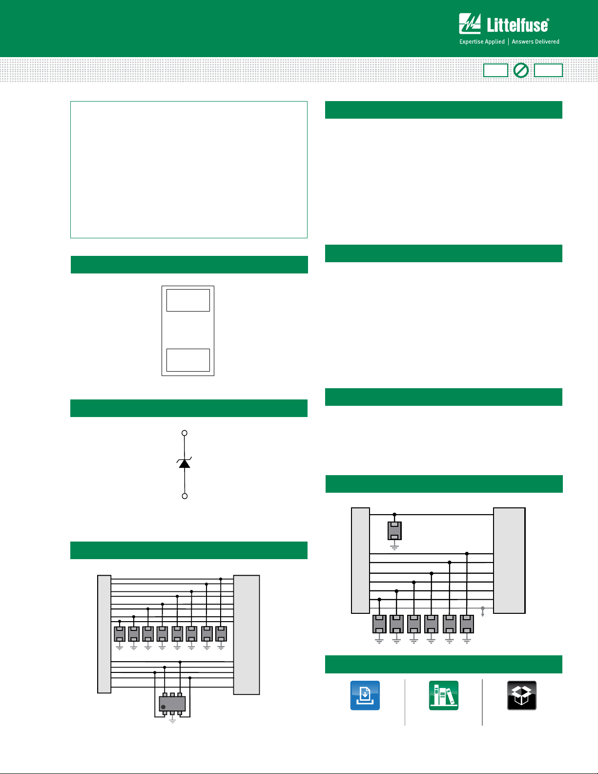
USB Port
USB Controller
Signal Ground
IC
*Packages are shown as transparent
SP1003
D+
D-
SSTX+
SSTX-
SSRX+
SSRX-
V
BUS
HDMI
Port
HDMI
Chipset
-
*Packages are shown as transparent
IC
SP3030 (x8)
SP3002
-
-
-
®
Diodes)
Low Capacitance ESD Protection - SP3030 Series
SP3030 Series 0.5pF 20kV Unidirectional Discrete TVS
Description
The SP3030 includes low capacitance rail to rail diodes
with an additional Zener diode to provide protection for
electronic equipment that may experience destructive
electrostatic discharges (ESD). These robust diodes
can safely absorb repetitive ESD strikes above the
maximum level specified in the IEC61000-4-2 international
standard (±20kV contact discharge) without performance
degradation. The low loading capacitance makes it ideal
for protecting high speed data lines such as HDMI, DVI,
USB2.0, USB3.0 and eSATA.
Features
Pinout
• ESD protection of ±20kV
contact discharge,
±30kV air discharge,
(IEC61000-4-2)
• EFT protection,
IEC61000-4-4, 40A
(t
=5/50ns)
p
• Lightning Protection,
IEC61000-4-5, 3A
(t
=8/20µs)
p
Pb
• Low capacitance of 0.5pF
@ V
=0V
R
• Low leakage current of
0.1μA at 5V
• Small SOD882 packaging
helps save board space
• AEC-Q101 qualied
(SOD882 package)
Applications
Functional Block Diagram
• Tablets
• Ultrabook
• eReader
• Smart Phones
• Digital Cameras
• MP3/ PMP
• Set Top Boxes
• Portable Medical
USB3.0 Application Example
Life Support Note:
Not Intended for Use in Life Support or Life Saving Applications
The products shown herein are not designed for use in life sustaining or life saving
applications unless otherwise expressly indicated.
HDMI Application Example
Additional Information
Datasheet
Resources
Samples
© 2013 Littelfuse, Inc.
Specifications are subject to change without notice.
Revised: 11/22/13
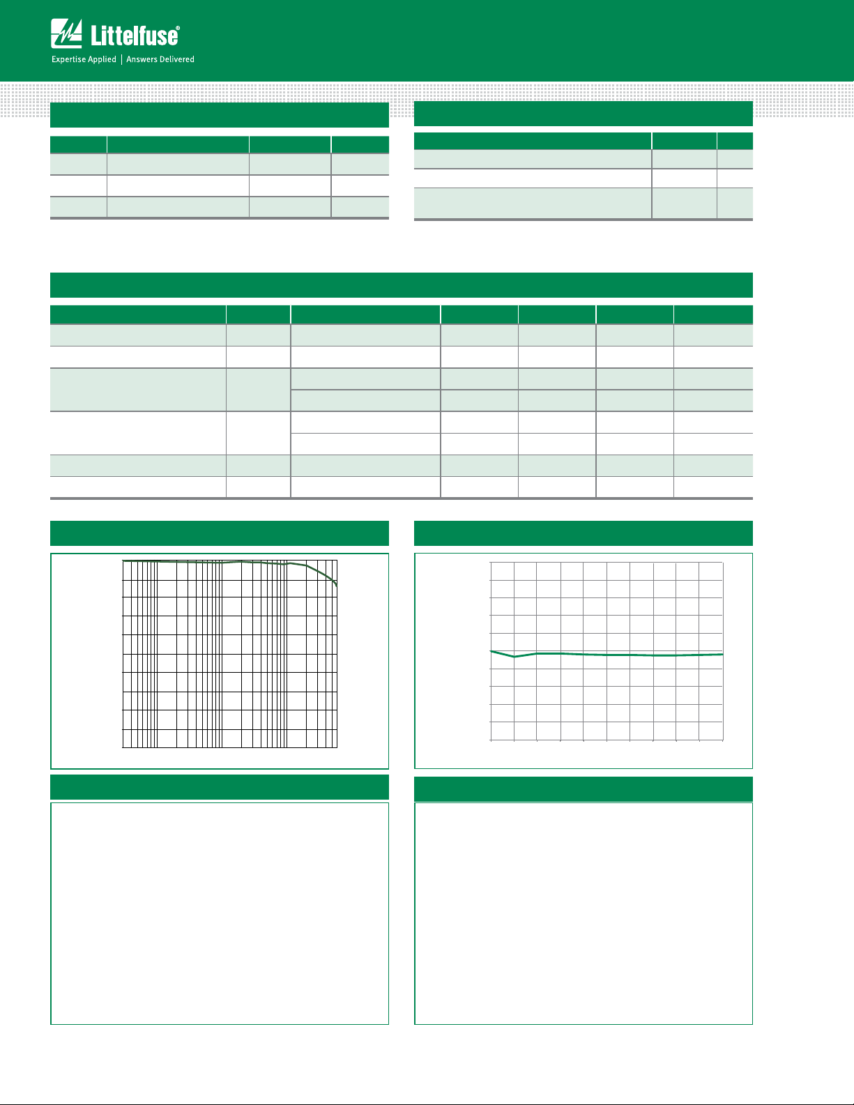
TVS Diode Arrays (SPA
Bias Voltage (V)
0.0 0.5 1.0 1.5 2.0 2.5 3.0 3.5 4.0 4.5 5.0
Normalized Capacitance (pF)
2.0
1.8
1.6
1.4
1.2
1.0
0.8
0.6
0.4
0.2
®
Diodes)
Low Capacitance ESD Protection - SP3030 Series
Absolute Maximum Ratings
Symbol Parameter Value Units
I
PP
T
OP
T
STOR
CAUTION: Stresses above those listed in “Absolute Maximum Ratings” may cause
permanent damage to the device. This is a stress only rating and operation of the device
at these or any other conditions above those indicated in the operational sections of this
specification is not implied.
Electrical Characteristics (T
Peak Current (tp=8/20μs) 3.0 A
Operating Temperature -40 to 125 °C
Storage Temperature -55 to 150 °C
=25ºC)
OP
Parameter Symbol Test Conditions Min Typ Max Units
Reverse Standoff Voltage V
Reverse Leakage Current I
Clamp Voltage
ESD Withstand Voltage
1
1
Dynamic Resistance R
Diode Capacitance
Note: 1. Parameter is guaranteed by design and/or device characterization.
1
C
RWM
LEAK
V
V
I/O-I/O
ESD
DYN
VR=5V with 1pin at GND 0.1 0.5 µA
IPP=1A, tp=8/20µs, Fwd 9.2 V
C
=2A, tp=8/20µs, Fwd 10.0 V
I
PP
IEC61000-4-2 (Contact) ±20 kV
IEC61000-4-2 (Air) ±30 kV
(VC2-VC1)/(I
Reverse Bias=0V, f=1 MHz 0.5 pF
Insertion Loss (S21) I/O to GND
Thermal Information
Parameter Rating Units
Storage Temperature Range -55 to 150 °C
Maximum Junction Temperature 150 °C
Maximum Lead Temperature
(Soldering 20-40s)
5 V
) 0.8 Ω
PP2-IPP1
Normalized Capacitance vs. Reverse Voltage
260 °C
SP3030
0
-1
-2
-3
-4
-5
-6
Attenuation (dB)
-7
-8
-9
-10
10 1001000
Frequency (MHz)
HDMI 1.4 Eye Diagram
USB3.0 Eye Diagram
Specifications are subject to change without notice.
© 2013 Littelfuse, Inc.
Revised: 11/22/13
 Loading...