

Page 1
TVS Diode Arrays (SPA
5 4 3 2 1
6 7 8 9 10
GND (Pins 3,8)
Pin 5
Pin 2
Pin 1
Pin 4
GND (Pins 3,8)
Pin 5
Pin 2
Pin 1
Pin 4
RoHS
GREEN
®
Diodes)
Low Capacitance ESD Protection - SP3010 Series
SP3010 Series 0.45pF Diode Array
Pinout
*Pins 6, 7, 9, 10 are not internally connected but should be connected to the trace.
Pb
Description
The SP3010 integrates 4 channels of ultra-low capacitance
rail-to-rail diodes and an additional zener diode to provide
protection for electronic equipment that may experience
destructive electrostatic discharges (ESD). This robust
device can safely absorb repetitive ESD strikes at the
maximum level specified in the IEC61000-4-2 international
standard (Level 4, ±8kV contact discharge) without
performance degradation. The extremely low loading
capacitance also makes it ideal for protecting high speed
signal pins such as HDMI, USB3.0, USB2.0, and IEEE 1394.
Features
• ESD, IEC61000-4-2,
±8kV contact, ±15kV air
• EFT, IEC61000-4-4, 40A
(5/50ns)
• Lightning, IEC61000-4-5,
3A (t
=8/20μs)
P
• Low capacitance of
0.45pF (TYP) per I/O
• Low leakage current of
0.1μA (TYP) at 5V
• Small form factor
μDFN( JEDEC MO-229)
package saves board
space
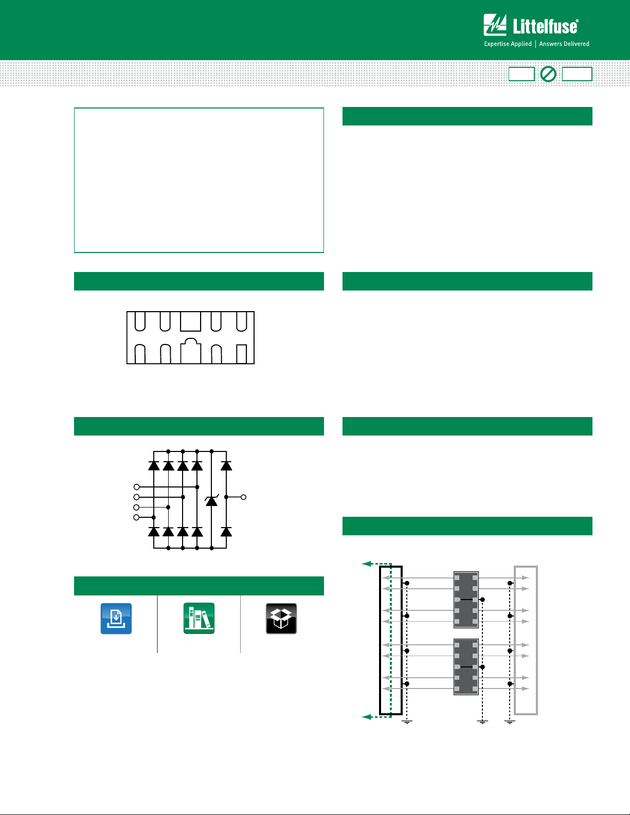
Functional Block Diagram
Additional Information
Datasheet
Life Support Note:
Not Intended for Use in Life Support or Life Saving Applications
The products shown herein are not designed for use in life sustaining or life saving
applications unless otherwise expressly indicated.
© 2013 Littelfuse, Inc.
Specifications are subject to change without notice.
Revised: 04/24/13
Resources
Samples
Applications
• LCD/PDP TVs
• DVD Players
• Desktops
• MP3/PMP
Application Example
HDMI
Port
Ground
SP3010-04
Ground
Ground
Outside World
SP3010-04
Ground
* Package is shown as transparent
Case
Ground
• Set Top Boxes
• Mobile Phones
• Notebooks
• Digital Cameras
HDMI
Chipset
D2+
D2-
D1+
D1-
D0+
D0-
CLK+
CLK-
Signal Ground
Page 2
TVS Diode Arrays (SPA
53
®
Diodes)
Low Capacitance ESD Protection - SP3010 Series
Absolute Maximum Ratings
Symbol Parameter Value Units
I
PP
T
OP
T
STOR
CAUTION: Stresses above those listed in “Absolute Maximum Ratings” may cause permanent damage to the device. This is a stress only rating and operation of
the device at these or any other conditions above those indicated in the operational sections of this specification is not implied.
Peak Current (tp=8/20μs) 3.0 A
Operating Temperature –40 to 125 °C
Storage Temperature –55 to 150 °C
Electrical Characteristics (T
OP
=25ºC)
Parameter Symbol Test Conditions Min Typ Max Units
Reverse Standoff Voltage V
Reverse Leakage Current I
Clamp Voltage
1
Dynamic Resistance R
ESD Withstand Voltage
Diode Capacitance
Note: 1 Parameter is guaranteed by design and/or device characterization.
0.6
0.5
0.4
0.3
0.2
I/O Capacitance (pF)
0.1
1
1
V
C
I/O-GND
RWM
LEAK
V
DYN
ESD
VR=5V, Any I/O to GND 0.1 0.5 µA
IPP=1A, tp=8/20µs, Fwd 10.8 V
C
I
PP
(VC2 - VC1) / (I
IEC61000-4-2 (Contact) ±8 kV
IR ≤ 1µA 6.0 V
=2A, tp=8/20µs, Fwd 12.3 V
- I
) 1. 5 Ω
PP2
PP1
IEC61000-4-2 (Air) ±15 kV
Reverse Bias=0V 0.45 pF
Insertion Loss (S21) I/O to GNDCapacitance vs. Bias Voltage
0
-5
-10
-15
Attenuation (dB)
-20
-25
0.0
0.00.5 1.01.5 2.02.5 3.03.5 4.04.5 5.0
I/O Bias Voltage (V)
Clamping Voltage vs. I
16.0
14.0
12.0
)
C
10.0
8.0
6.0
Clamp Voltage (V
4.0
2.0
0.0
PP
1.51.02.0 2.
Peak Pulse Current-I
(A)
PP
-30
10 100 1000 10000
Frequency (MHz)
Pulse Waveform
110%
100%
90%
80%
70%
PP
60%
50%
40%
Percent of I
30%
20%
10%
0%
.0
0.05.0 10.0 15.0 20.0 25.0 30.0
Time (μs)
Specifications are subject to change without notice.
© 2013 Littelfuse, Inc.
Revised: 04/24/13
Page 3

TVS Diode Arrays (SPA
t
R
R
o
C
e
T
SP
3010
04 U T
G
Series
Package
µDFN-10 (2.5x1.0mm)
T= Tape & Reel
G= Green
Number of
Channels
-04 = 4 Channel
TVS Diode Arrays
(SPA
®
Diodes)
Q
*
4
Product Series
Q = SP3010
Assembly Site
Number o
f
Channels
®
Diodes)
Low Capacitance ESD Protection - SP3010 Series
Soldering Parameters
Reflow Condition Pb – Free assembly
Pre Heat
- Temperature Min (T
- Temperature Max (T
) 150°C
s(min)
) 200°C
s(max)
- Time (min to max) (ts) 60 – 180 secs
Average ramp up rate (Liquidus) Temp
(T
) to peak
L
to TL - Ramp-up Rate 3°C/second max
T
S(max)
Reflow
- Temperature (TL) (Liquidus) 217°C
- Temperature (tL) 60 – 150 seconds
Peak Temperature (TP) 260
Time within 5°C of actual peak
Temperature (t
)
p
3°C/second max
+0/-5
°C
20 – 40 seconds
Ramp-down Rate 6°C/second max
Time 25°C to peak Temperature (T
) 8 minutes Max.
P
Do not exceed 260°C
Part Numbering System
T
P
Ramp-up
t
amp-up
PreheatPrehea
S
T
L
T
S(max)
Temperature
T
S(min)
25
time to peak temperature
Product Characteristics
Lead Plating Pre-Plated Frame
Lead Material Copper Alloy
t
P
t
L
Critical Zone
ritical Zon
L to TP
to
T
Ramp-down
amp-d
Time
© 2013 Littelfuse, Inc.
Specifications are subject to change without notice.
Revised: 04/24/13
Part Marking System
Ordering Information
Part Number Package Marking Min. Order Qty.
SP3010-04UTG
µDFN-10
Q*4 3000
Lead Coplanarity 0.0004 inches (0.102mm)
Substitute Material Silicon
Body Material Molded Epoxy
Flammability UL 94 V-0
Notes :
1. All dimensions are in millimeters
2. Dimensions include solder plating.
3. Dimensions are exclusive of mold flash & metal burr.
4. Blo is facing up for mold and facing down for trim/form, i.e. reverse trim/form.
5. Package surface matte finish VDI 11-13.
Page 4

TVS Diode Arrays (SPA
K0
A0
B0
P2
P1
P0
T
F
E
W
D0
D1
5º Max
5º Max
User Feeding Direction
Pin 1 Location
D
E
B
Top View
A
A
Bottom View
0.05 C
b
A1
b1
A3
C
Seating
Plane
Side View
0.10
C
A
M
B
0.05
C
M
L
e
2xR0.075mm (7x)
R0.125
0.05 C
D
E
B
Top View
A
A
Bottom View
b
A1
b1
A3
C
Side View
0.10
C
A
M
B
0.05
C
M
L
e
2xR0.075mm (7x)
R0.125
0.05 C
X1
X
P
P1
Z (C) G
Y
(Y1)
Soldering Pad Layout
Recomended
X1
X
P
P1
Z (C) G
Y
(Y1)
Soldering Pad Layout
Alternative
Low Capacitance ESD Protection - SP3010 Series
Embossed Carrier Tape & Reel Specification — µDFN-10
®
Diodes)
Package Dimensions — µDFN-10 (2.5x1.0x0.5mm)
Package
Symbol Millimeters
A0 1.30 ± 0.10
B0 2.83 ± 0.10
D0 Ø 1.50 + 0.10
D1 Ø 1.00 + 0.25
E 1.75 ± 0.10
F 3.50 ± 0.05
K0 0.65 ± 0.10
P0 4.00 ± 0.10
P1 4.00 ± 0.10
P2 2.00 ± 0.05
T 0.254 ± 0.02
W 8.00 + 0.30 /- 0.10
Package
JEDEC MO-229
Symbol
A 0.48 0.515 0.55 0.019 0.020 0.021
A1 0.00 -- 0.05 0.000 0.022
A3 0.125 Ref 0.005 Ref
b 0.15 0.20 0.25 0.006 0.008 0.012
b1 0.35 0.40 0.45 0.014 0.016 0.018
D 2.40 2.50 2.60 0.094 0.098 0.102
E 0.90 1. 0 0 1. 10 0.035 0.039 0.043
e 0.50 BSC 0.020 BSC
L 0.30 0.365 0.43 0.012 0.014 0.016
Min Nom Max Min Nom Max
µDFN-10 (2.5x1.0x0.5mm)
Millimeters Inches
µDFN-10 (2.5x1.0x0.5mm)
Soldering Pad Layout Dimensions
Inch Millimeter
C (0.034) (0.875)
G 0.008 0.20
P 0.020 0.50
P1 0.039 1. 0 0
X 0.008 0.20
X1 0.016 0.40
Y 0.027 0.675
Y1 (0.061) (1.55)
Z 0.061 1.55
Specifications are subject to change without notice.
© 2013 Littelfuse, Inc.
Revised: 04/24/13
 Loading...