

TVS Diode Arrays (SPA
RoHS
GREEN
®
Diodes)
Low Capacitance ESD Protection - SP3004 Series
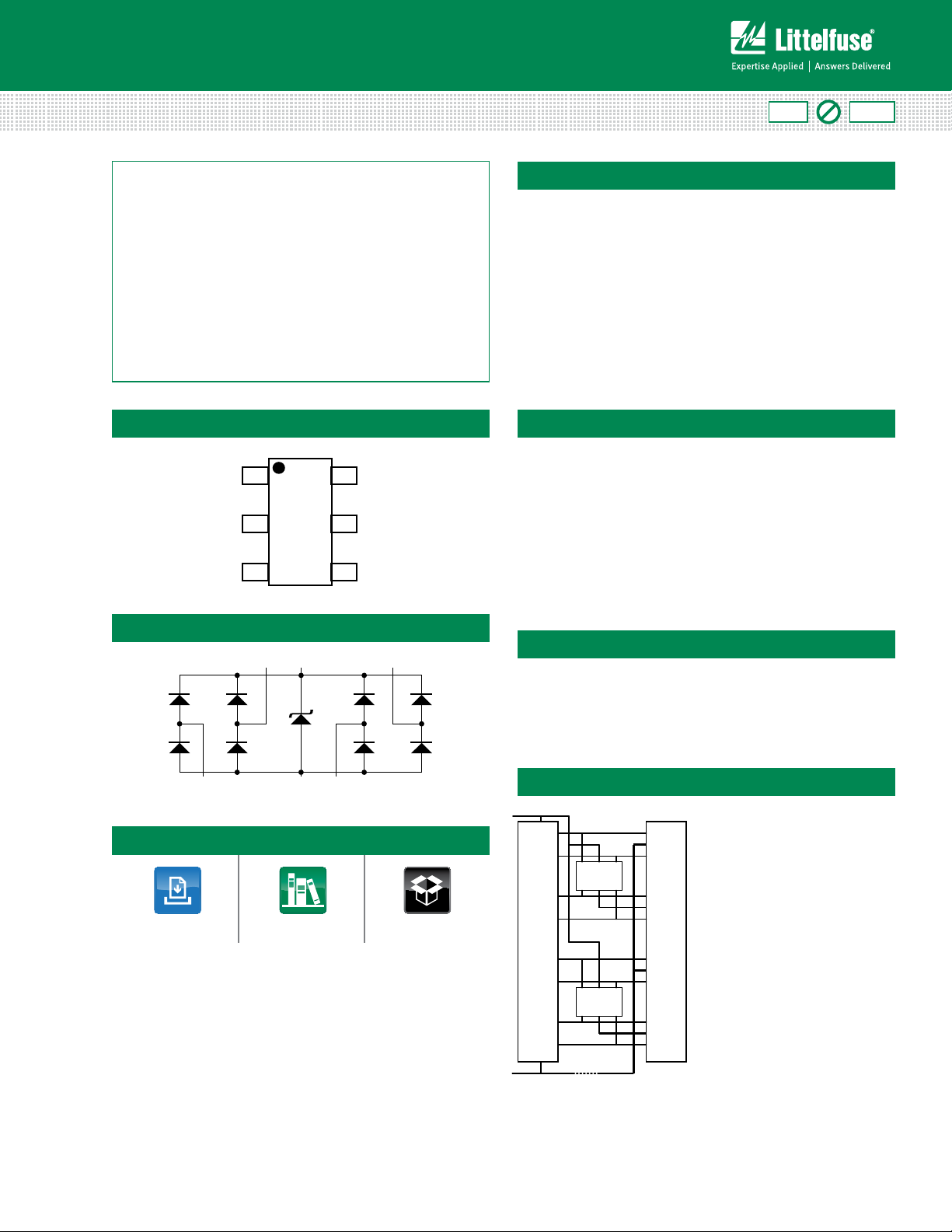
SP3004 Series 0.85pF Diode Array
Pinout
I/O 1
GND
I/O 2
I/O 4
V
CC
I/O 3
Pb
Description
The SP3004 has ultra low capacitance rail-to rail diodes
with an additional zener diode fabricated in a proprietary
silicon avalanche technology to protect each I/O pin
providing a high level of protection for electronic equipment
that may experience destructive electrostatic discharges
(ESD). These robust diodes can safely absorb repetitive
ESD strikes at the maximum level (Level 4) specified in the
IEC 61000-4-2 international standard without performance
degradation. Their very low loading capacitance also makes
them ideal for protecting high speed signal pins such as
HDMI, DVI, USB2.0, and IEEE 1394.
Features
• Low capacitance of
0.85pF (TYP) per I/O
• ESD protection of ±12kV
contact discharge,
±15kV air discharge,
(IEC61000-4-2)
• EFT protection,
IEC61000-4-4, 40A
(5/50ns)
• Low leakage of 1nA MAX
with V
=3.3V
R
• Small SOT563 package
saves board space
• Lightning Protection,
IEC61000-4-5, 4A
(8/20µs)
Functional Block Diagram
I/O2
I/O1
Additional Information
Datasheet
Resources
V
CC
GND
I/O3
I/O4
Samples
Applications
• Computer Peripherals
• Mobile Phones
• PDA’s
• Digital Cameras
Application Example
+5V
D2+
D2-
D1+
D1-
HDMI
or DVI
Interface
D0+
D0-
Clk+
Clk-
6 5 4
SP300x-04
1 2 3
IC
6 5 4
SP300x-04
1 2 3
Gnd
D2+
Gnd
D2-
D1+
Gnd
D1-
HDMI
or DVI
Connector
D0+
Gnd
D0-
Clk+
Gnd
Clk-
• Network Hardware/Ports
• Test Equipment
• Medical Equipment
A single 4 channel SP300x-04
device can be used to protect
four of the data lines in a
HDMI/DVI interface. Two (2)
SP300x-04 devices provide
protection for the main data
lines. Low voltage ASIC
HDMI/DVI drivers can also be
protected with the SP300x-04,
the +V
pins on the SP300x-04
CC
can be substituted with a
suitable bypass capacitor or in
some backdrive applications the
+V
of the SP300x-04 can be
CC
floated or NC.
Life Support Note:
Not Intended for Use in Life Support or Life Saving Applications
The products shown herein are not designed for use in life sustaining or life saving
applications unless otherwise expressly indicated.
© 2013 Littelfuse, Inc.
Specifications are subject to change without notice.
Revised: 04/24/13
TVS Diode Arrays (SPA
®
Diodes)
Low Capacitance ESD Protection - SP3004 Series
Absolute Maximum Ratings
Symbol Parameter Value Units
I
PP
T
OP
T
STOR
CAUTION: Stresses above those listed in “Absolute Maximum Ratings” may cause
permanent damage to the device. This is a stress only rating and operation of the device
at these or any other conditions above those indicated in the operational sections of this
specification is not implied.
Electrical Characteristics (T
Reverse Standoff Voltage V
Reverse Leakage Current
Clamp Voltage
ESD Withstand Voltage
Dynamic Resistance R
Diode Capacitance
Diode Capacitance
Note: 1 Parameter is guaranteed by design and/or device characterization.
Peak Current (tp=8/20μs) 4 A
Operating Temperature –40 to 125 °C
Storage Temperature –55 to 150 °C
=25ºC)
OP
Parameter Symbol Test Conditions Min Typ Max Units
RWM
1
1
1
1
1
I
V
C
I/O-GND
C
LEAK
V
C
ESD
DYN
I/O-I/O
IR ≤ 1µA 6 V
VR=3.3V 1 nA
IPP=1A, tp=8/20µs, Fwd 10.0 12.0 V
=2A, tp=8/20µs, Fwd 11. 8 15.0 V
I
PP
IEC61000-4-2 (Contact) ±12 kV
IEC61000-4-2 (Air) ±15 kV
(VC2 - VC1) / (I
Reverse Bias=0V 0.95 1. 1 1.25 pF
Reverse Bias=1.65V 0.7 0.85 1 pF
Reverse Bias=0V 0.5 pF
Thermal Information
Parameter Rating Units
Storage Temperature Range –55 to
Maximum Junction Temperature 150 °C
Maximum Lead Temperature
(Soldering 20-40s)
- I
) 1. 8 Ω
PP2
PP1
150
°C
260 °C
0
-5
-10
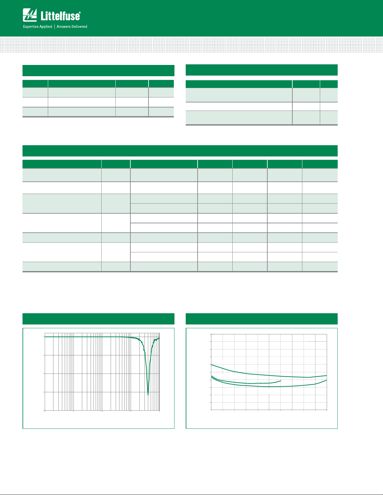
Insertion Loss [dB]
-15
-20
1.E+06 1.E+07 1.E+08 1.E+09 1.E+10
Frequency [Hz]
Capacitance vs. Bias VoltageInsertion Loss (S21) I/O to GND
1.50
1.40
1.30
1.20
1.10
1.00
0.90
0.80
I/O Capacitance (pF)
0.70
0.60
0.50
0.0 0.5 1.01.5 2.0 2.5 3.0 3.5 4.0 4.5 5.0
V
= Float
CC
VCC = 3.3V
VCC = 5V
I/O DC Bias (V)
Specifications are subject to change without notice.
© 2013 Littelfuse, Inc.
Revised: 04/24/13
 Loading...