

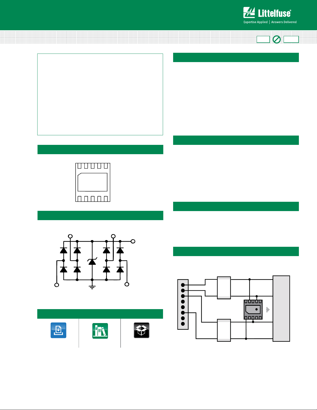
TVS Diode Arrays (SPA
GND
13
97
5
13 5
79
GND
J1
J8
RJ-45 Connector
*Package is shown as transparent Ethernet PHY
Tx+
Tx-
Rx-
Rx+
SP2504N
PHY
®
Diodes)
Lightning Surge Protection - SP2504N Series
SP2504N Series 2.5V 20A Diode Array
Pinout
RoHS
Pb
GREEN
Description
The SP2504N integrates 4 channels of low capacitance
diodes with an additional zener diode to protect sensitive
I/O pins against lightning induced surge events and
ESD. This robust device can safely absorb up to 20A per
IEC61000-4-5 (t
=8/20μs) without performance degradation
P
and a minimum ±30kV ESD per IEC61000-4-2 international
standard. The low loading capacitance makes the SP2504N
ideal for protecting high-speed signal pins.
Features
• ESD, IEC61000-4-2,
±30kV contact, ±30kV air
• EFT, IEC61000-4-4, 40A
(t
p
=5/50ns)
• Low capacitance of 3.5pF
(TYP) per I/O
• Low leakage current of
1µA (MAX) at 2.5V
• Lightning, IEC61000-4-5,
20A (t
p
=8/20µs)
Functional Block Diagram
Additional Information
Datasheet
Resources
Samples
Applications
• 10/100/1000 Ethernet
Interfaces
• Customer Premise
Equipment (CPE)
Application Example
• VoIP Phones
• Set Top Boxes
• PBX Systems
Life Support Note:
Not Intended for Use in Life Support or Life Saving Applications
The products shown herein are not designed for use in life sustaining or life saving
applications unless otherwise expressly indicated.
© 2013 Littelfuse, Inc.
Specifications are subject to change without notice.
Revised: 04/24/13
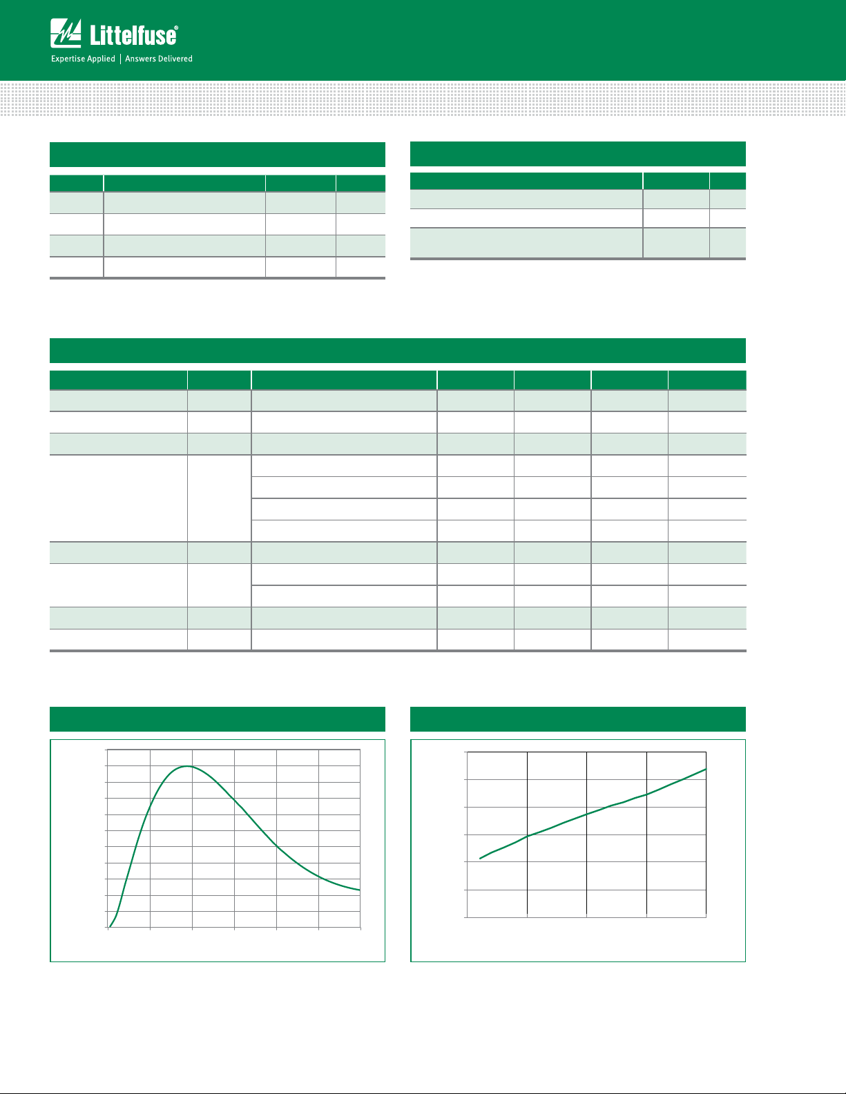
TVS Diode Arrays (SPA
0%
10%
20%
30%
40%
50%
60%
70%
80%
90%
100%
110%
0.0 5.0 10.0 15.0 20.0 25.0 30.0
Time (μs)
Percent of I
PP
0.0
2.0
4.0
6.0
10.0
12.0
Peak Pulse Current-I
PP
(A)
0 5 10 15 20
8.0
Clamp Voltage (V
C
)
®
Diodes)
Lightning Surge Protection - SP2504N Series
Absolute Maximum Ratings
Symbol Parameter Value Units
I
PP
P
PK
T
OP
T
STOR
CAUTION: Stresses above those listed in “Absolute Maximum Ratings” may cause
permanent damage to the device. This is a stress only rating and operation of the device
at these or any other conditions above those indicated in the operational sections of this
specification is not implied.
Electrical Characteristics (T
Reverse Standoff Voltage V
Snap Back Voltage V
Reverse Leakage Current I
Clamp Voltage
Dynamic Resistance R
ESD Withstand Voltage
Diode Capacitance
Diode Capacitance
Peak Current (tp=8/20μs) 20.0 A
Peak Pulse Power (tp=8/20µs) 300 W
Operating Temperature –40 to 125 ºC
Storage Temperature –55 to 150 °C
=25ºC)
OP
Parameter Symbol Test Conditions Min Typ Max Units
RWM
SB
LEAK
ISB=50mA 2.0 V
VR=2.5V, I/O to GND 0.5 1. 0 µA
IPP=1A, tp=8/20µs, Fwd 5.0 V
I
=5A, tp=8/20µs, Fwd 6.3 V
1
1
1
1
V
C
I/O-GND
C
V
C
DYN
ESD
I/O-I/O
PP
I
=10A, tp=8/20µs, Fwd 8.0 V
PP
I
=20A, tp=8/20µs, Fwd 11. 5 V
PP
(VC2-VC1)/(I
PP2-IPP1
IEC61000-4-2 (Contact) ±30 kV
IEC61000-4-2 (Air) ±30 kV
Reverse Bias=0V 3.5 5.0 pF
Reverse Bias=0V 2.0 pF
Thermal Information
Parameter Rating Units
Storage Temperature Range –55 to 150 °C
Maximum Junction Temperature 150 °C
Maximum Lead Temperature
(Soldering 20-40s)
2.5 V
) 0.35
260 °C
W
Note: 1. Parameter is guaranteed by design and/or device characterization.
Pulse Waveform
Clamping Voltage vs. I
PP
Specifications are subject to change without notice.
© 2013 Littelfuse, Inc.
Revised: 04/24/13
 Loading...