


TVS Diode Arrays (SPA
RoHS
GREEN
®
Diodes)
General Purpose ESD Protection - SP1005 Series
SP1005 Series 30pF 30kV Bidirectional Discrete TVS
Description
The SP1005 includes back-to-back Zener diodes fabricated
in a proprietary silicon avalanche technology to provide
protection for electronic equipment that may experience
destructive electrostatic discharges (ESD). These robust
diodes can safely absorb repetitive ESD strikes above the
maximum level specified in the IEC61000-4-2 international
standard (Level 4, ±8kV contact discharge) without
performance degradation. The back-to-back configuration
provides symmetrical ESD protection for data lines when
AC signals are present.
Pinout
0201 Flipchip
12
SOD882
Features
• ESD, IEC61000-4-2,
±30kV contact, ±30kV air
• EFT, IEC61000-4-4, 40A
(5/50ns)
• Lightning, IEC61000-4-5,
10A (t
=8/20μs)
P
• Low capacitance of 30pF
(@ V
=0V)
R
Pb
• Low leakage current of
0.1μA at 5V
• Space efcient 0201 and
0402 footprint
• AEC-Q101 qualied
(SOD882 package)
1
(AEC-Q101 qualified)
Functional Block Diagram
1
Additional Information
Datasheet
Resources
Applications
2
• Mobile Phones
• Smart Phones
• Camcorders
• Portable Medical
• Digital Cameras
• MP3/PMP
• Portable Navigation
Devices
• Tablets
• Point of Sale Terminals
Application Example
I/O Controller
ICP3
2
Samples
Outside
World
Keypads
P1
P2
P4
SP1005 (x4)
GND
Life Support Note:
Not Intended for Use in Life Support or Life Saving Applications
The products shown herein are not designed for use in life sustaining or life saving
applications unless otherwise expressly indicated.
© 2013 Littelfuse, Inc.
Specifications are subject to change without notice.
Revised: 11/22/13
TVS Diode Arrays (SPA
0.0
5.0
10.0
15.0
20.0
25.0
30.0
35.0
40.0
0.0 0.5 1.01.5 2.0 2.5 3.0 3.5 4.0 4.5 5.0
Bias Voltage (V)
Capacitance (pF)
0%
10%
20%
30%
40%
50%
60%
70%
80%
90%
100%
110%
0.0 5.0 10.0 15.0 20.0 25.0 30.0
Time (μs)
Percent of I
PP
®
Diodes)
General Purpose ESD Protection - SP1005 Series
Absolute Maximum Ratings
Symbol Parameter Value Units
1
I
PP
T
OP
T
STOR
Notes:
1. “1 “ indicates SP1005-01WTG , while “2” indicates SP1005-01ETG
2. CAUTION: Stresses above those listed in “Absolute Maximum Ratings” may cause permanent damage to the device. This is a stress only rating and operation
of the device at these or any other conditions above those indicated in the operational sections of this specification is not implied.
Peak Current (tp=8/20μs)
Operating Temperature –40 to 125 °C
Storage Temperature –55 to 150 °C
Thermal Information
Parameter Rating Units
Storage Temperature Range –55 to 150 °C
Maximum Junction Temperature 150 °C
Maximum Lead Temperature (Soldering 20-40s) 260 °C
10.0
8.0
2
A
Electrical Characteristics (T
OP
=25ºC)
Parameter Symbol Test Conditions Min Typ Max Units
Reverse Standoff Voltage V
Breakdown Voltage V
Leakage Current I
Clamp Voltage
1
Dynamic Resistance R
ESD Withstand Voltage
Diode Capacitance
Note:
1
Parameter is guaranteed by design and/or device characterization.
1
1
V
RWM
BR
LEAK
V
DYN
ESD
C
C
IEC61000-4-2 (Contact Discharge) ±30 kV
IEC61000-4-2 (Air Discharge) ±30 kV
D
6.0 V
IR=1mA 8.5 9.5 V
VR=5V with 1 pin at GND 0.1 0.5 μA
IPP=1A, tp=8/20µs, Fwd 9.3 V
I
=2A, tp=8/20µs, Fwd 10.0 V
PP
I
=10A, tP=8/20μs, Fwd 15.6 V
PP
(VC2 - VC1) / (I
- I
) 0.7 Ω
PP2
PP1
Reverse Bias=0V 30 pF
Reverse Bias=2.5V 23 pF
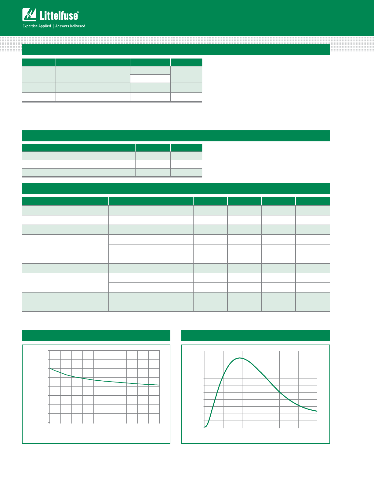
Pulse WaveformCapacitance vs. Reverse Bias
Specifications are subject to change without notice.
© 2013 Littelfuse, Inc.
Revised: 11/22/13
 Loading...