

LITTELFUSE SMT50-100, SMT50-120, SMT50-130, SMT50-180, SMT50-200 Datasheet
...
48
www.littelfuse.com
SMT50
The electrical characteristics of a SMT50 device are similar to
that of a self-gated Triac, but the SMT50 is a two terminal
device with no gate. The gate function is achieved by an
internal current controlled mechanism.
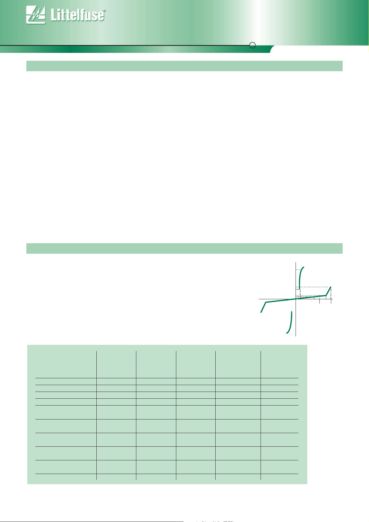
Like the T.V.S. diodes, the SMT50 has a standoff voltage (Vrm)
which should be equal to or greater than the operating
voltage of the system to be protected. At this voltage (Vrm)
the current consumption of the SMT50 is negligible and will
not affect the protected system.
When a transient occurs, the voltage across the SMT50 will
increase until the breakdown voltage (Vbr) is reached. At this
point the device will operate in a similar way to a T.V.S.
device and is in avalanche mode.
The voltage of the transient will now be limited and will only
increase by a few volts as the device diverts more current. As
this transient current rises, a level of current through the
device is reached (Ibo) which causes the device to switch to a
fully conductive state such that the voltage across the device
is now only a few volts (Vt). The voltage at which the device
switched from the avalanche mode to the fully conductive
state (Vt) is known as the Breakover voltage (Vbo). When the
device is in the Vt state, high currents can be diverted
without damage to the SMT50 due to the low voltage across
the device, since the limiting factor in such devices is
dissipated power (V x I).
Resetting of the device to the non-conducting state is
controlled by the current flowing through the device. When
the current falls below a certain value, known as the Holding
Current (Ih), the device resets automatically.
As with the avalanche T.V.S. device, if the SMT50 is subjected
to a surge current which is beyond its maximum rating, then
the device will fail in short circuit mode, ensuring that the
equipment is ultimately protected.
SELECTING A SMT50
COMPLIES WITH THE PEAK SURGE VOLTAGE CURRENT ADMISSIBLE IPP NECESSARY
FOLLOWING STANDARDS VOLTAGE WAVEFORM WAVEFORM RESISTOR
(V) (
µS) (µS) (A) (Ω)
(CCITT) ITU-K20 1000 10/700 5/310 25 -
(CCITT) ITU-K17 1500 10/700 5/310 38 -
-
VDE0433 2000 10/700 5/310 50
VDE0878 2000 1.2/50 1/20 50 -
IEC-1000-4-5 10/700 5/310 50 -
level 4
level 3
1.2/500 8/20 100 -
FCC Part 68, lightning surge 1500 10/160 10/160 75 12.5
type A 800 10/560 10/560 55 6.5
FCC Part 68, lightning surge 1000 9/720 5/320 25 -
type B
Bellcore TR-NWT-001089 2500 2/10 2/10 150 11.5
first level 1000 10/1000 10/1000 50 10
Bellcore TR-NWT-001089 5000 2/10 2/10 150 11.5
second level
CNET I31-24 1000 0.5/700 0.8/310 25 -
V
R
V
BR
V
RM
V
BO
I
RM
I
BO
I
H
I
pp
I
V
1. When selecting a SMT50 device, it is important that
the Vrm of the device is equal to or greater than the
the operating voltage of the system.
2. The minimum Holding Current (Ih) must be greater
than the current the system is capable of delivering
otherwise the device will remain conducting following
a transient condition.
V-I Graph illustrating symbols
and terms for the SMT50 surge
protection device.
ELECTRICAL CHARACTERISTICS
www.littelfuse.com
49
ELECTRICAL CHARACTERISTICS (Tamb 25°C)
ABSOLUTE MAXIMUM RATINGS (Tamb 25°C)
THERMAL RESISTANCE
SYMBOL PARAMETER SYMBOL PARAMETER
V
RM
Stand-off Voltage V
BO
Breakover Voltage
I
RM
Leakage Current at Stand-off Voltage I
H
Holding Current
V
R
Continuous Reverse Voltage I
BO
Breakover Current
V
BR
Breakdown Voltage I
PP
Peak pulse Current
C Capacitance
SYMBOL PARAMETER VALUE UNIT
R
TH
(J-I) Junction to leads 20 °C/W
R
TH
(J-I) Junction to ambient on printed circuit 100 °C/W
(with standard footprint dimensions)
SYMBOL PARAMETER VALUE UNIT
P Power dissipation Tlead 5W
I
PP
Peak pulse current 10/1000µS 50 A
8/20µS 100 A
I
TSM
Non repetitive surge peak on-state current tp + 20ms 30 A
dV/dt Critical rate of rise of off-state voltage V
RM 5
KV/µS
T
stg Storage temperature range -55 to +150 °C
Tj Maximum junction temperature 150 °C
T
L Maximum lead temperature for soldering during 10s 260 Tstg
Type
SMT50-62
SMT50-68
SMT50-100
SMT50-120
SMT50-130
SMT50-180
SMT50-200
SMT50-220
SMT50-240
SMT50-270
Marking
Laser
A062
A068
A100
A120
A130
A180
A200
A220
A240
A270
IRM @ VRM
MAX
(µA) (V)
IRM @ VR
MAX
(µA) (V)
62
68
100
120
130
180
200
220
240
270
50
50
50
50
50
50
50
50
50
50
800
800
800
800
800
800
800
800
800
800
82
90
133
160
173
240
267
293
320
360
56
60
90
180
117
162
180
198
216
243
2
2
2
2
2
2
2
2
2
2
VBO @ IBO
MAX
(V) (mA)
IH
MIN
(Note 1)
(mA)
150
150
150
150
150
150
150
150
150
150
C
MAX
(pF)
150
150
100
100
100
100
100
100
100
100
All parameters are tested @ 25°C except where indicated.
Note 1: Measured @ 1V bias, 1MHZ All parameters are tested using a FET TEST
TM
model 3600
SMT50
 Loading...