

LITTELFUSE PGB002ST23WR Datasheet
4
PULSEGUARD
®
SUPPRESSORS
PulseGuard®Suppressors
177
www.littelfuse.com
Polymeric ESD Suppressors
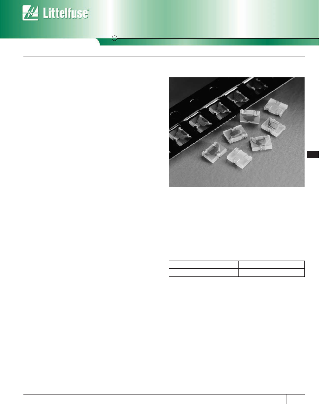
PGB Series SOT23 Surface Mount ESD Suppressor
Product Overview
PulseGuard ESD Suppressors help protect sensitive electronic
equipment against electrostatic discharge (ESD). They supplement the
on-chip protection of integrated circuitry and are best suited for lowvoltage, high-speed applications where low capacitance is important.
Data ports utilizing such high-speed protocols as USB 2.0, IEEE1394
and InfiniBandSMcan benefit from this new technology. PulseGuard
suppressors use polymer composite materials to suppress fast-rising
ESD transients (as specified in IEC 61000-4-2 and MIL-STD-883E).
Features
• Ultra-low capacitance
• Low leakage current
• Fast response time
• 2-lines of protection
• Bi-directional
• Withstands multiple ESD strikes
• Standard JEDEC SOT23 outline
• Compatible with pick-and-place processes
• Available in 3,000 piece reels
Typical Applications
• Servers
• Laptop/Desktop Computers
• Network Hardware
• Computer Peripherals
• Digital Cameras
• External Storage
Electrical Characteristics
Trigger Voltage1. . . . . . . . . . . . . . . . . . . . . . . . . . . . . . . . 1,000V typical
Clamping Voltage1. . . . . . . . . . . . . . . . . . . . . . . . . . . . . . . . 150V typical
Rated Voltage . . . . . . . . . . . . . . . . . . . . . . . . . . . . . . . . . . . 24VDC max
Capacitance2. . . . . . . . . . . . . . . . . . . . . . . . . . . . . . . . . . . . . . 0.055pF
Response Time1. . . . . . . . . . . . . . . . . . . . . . . . . . . . . . . . . . . . . . . <1ns
Leakage Current3. . . . . . . . . . . . . . . . . . . . . . . . . . . . . . . . . . . . . <1nA
ESD Pulse Withstand1. . . . . . . . . . . . . . . . . . . . . 1,000 pulses minimum
Notes:
1. 8 kV direct discharge method, per IEC 61000-4-2.
2. Measured at 1 MHz.
3. Measured at 6 VDC. Testing at fast ESD pulse rates (1-20Hz) may
cause a change in leakage current performance (6µA, max).
Physical Specifications
Materials:
Body: Glass Epoxy
Terminations: Tin-Lead
Soldering Parameters:
Wave solder -- 260°C, 10 seconds maximum
Reflow solder -- 260°C, 30 seconds maximum
Operating Temperature Range:
-65°C to 125°C
Ordering Information
CATALOG NUMBER PIECES PER REEL
PGB002ST23WR 3,000
Design Consideration
Because of the fast rise-time of the ESD transient, placement of
PulseGuard suppressors is a key design consideration. To achieve
optimal ESD suppression, the devices should be placed on the circuit
board as close to the source of the ESD transient as possible. Install
PulseGuard suppressors directly behind the connector so that they are
the first board-level circuit component encountered by the ESD transient.
They are connected from signal/data line to ground.
Next
Previous
Polymeric ESD Suppressors
PGB Series SOT23 Surface Mount ESD Suppressor
PulseGuard®Suppressors
178
www.littelfuse.com
Definitions
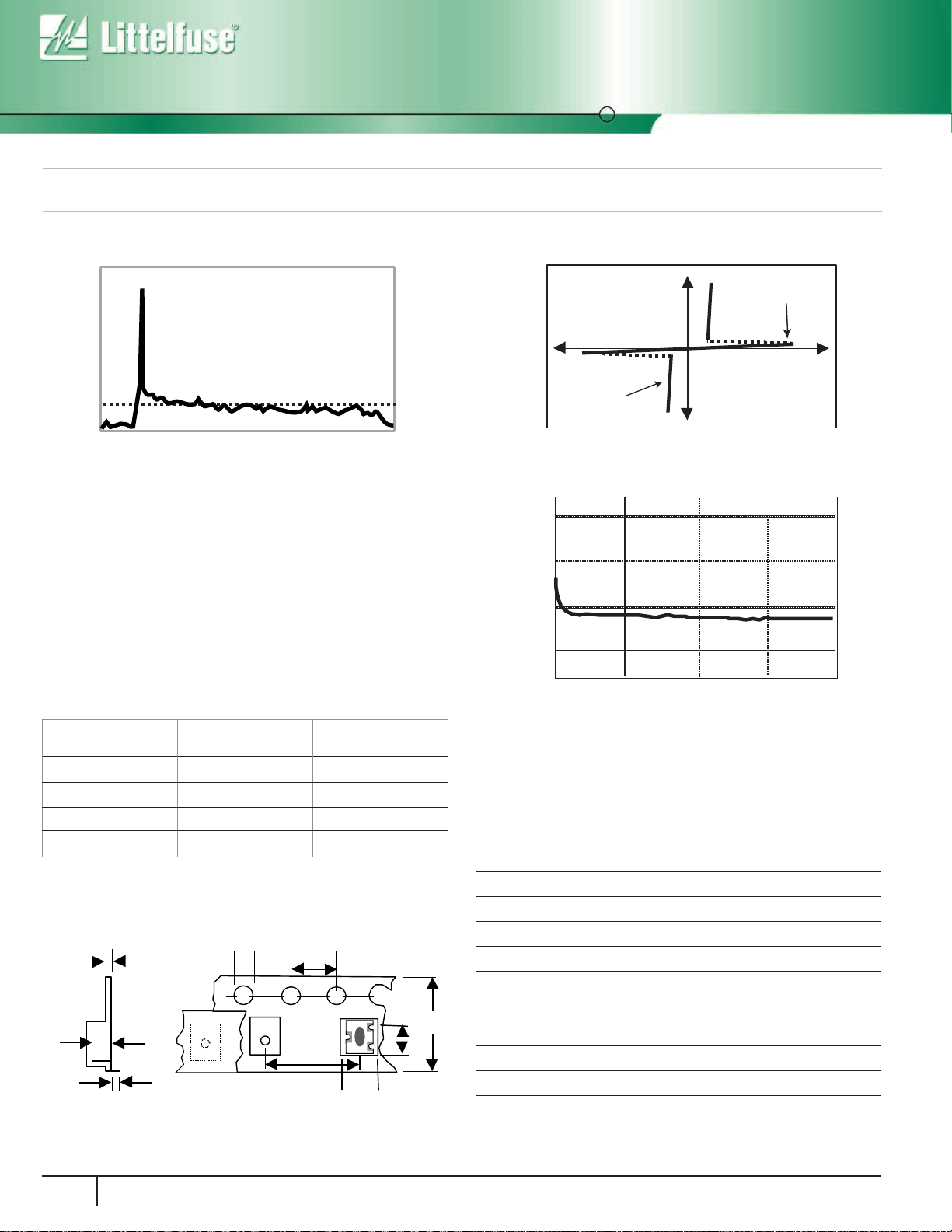
Trigger Voltage: The measured peak voltage across the ESD
suppressor before it transitions from high to low resistance. It is
manifested as a “spike” before the clamping voltage is achieved.
This voltage is typically well below the damage threshold of on-chip
IC protection.
Clamping Voltage: The voltage level to which the ESD impulse voltage
is reduced. This is the voltage that the suppressor holds at, until the ESD
transient energy is dissipated.
ESD Impulse Voltage: Also known as the ESD Threat Voltage. This is
the voltage that is “zapped” into the circuit. Voltages generated by people
can exceed 15 kV. The IEC 61000-4-2 defines four levels of impulse
voltage for testing purposes:
Capacitance vs. Frequency
Generalized PulseGuard Suppressor Response to ESD
(Positive and Negative Polarity ESD Pulses)
Generalized I-V Curve
(Positive and Negative Polarity ESD Pulses)
SEVERITY LEVEL
1
2
3
4
AIR DISCHARGE
2 kV
4 kV
8 kV
15 kV
DIRECT
DISCHARGE
2 kV
4 kV
6 kV
8 kV
Carrier Tape Specifications
Parts are delivered on 7” (178mm) reel, plastic carrier tape
DESCRIPTION
Ct- Cover tape thickness
Dd- Drive hole diameter
Ds- Drive hole spacing
Pd- Pocket depth
Ph- Pocket height
P
s - Pocket spacing
P
w
- Pocket width
Tt- Carrier tape thickness
Tw- Carrier tape width
MEASUREMENT (MM)
0.06
1.50
4.00
1.02
3.23
4.00
2.46
0.30
8.00
Next
Previous
Trigger Voltage
Voltage (V)
Clamping Voltage
Time (ns)
Current (A)
Clamping
Voltage
Voltage (V)
70
60
50
Capacitance (fF)
40
1.0
Frequency (GHz)
Trigger
Voltage
** Note: 1,000 fF = 1 pF
2.01.50.5
T
t
D
D
d
P
d
C
t
+
+
s
++++
P
s
P
w
T
w
P
h
 Loading...