

Page 1
Transient Voltage Suppression Diodes
Axial Leaded – 600W > P6KE series
P6KE Series
Bi-directional
Uni-directional
Agency Approvals
AGENCY AGENCY FILE NUMBER
E128662/E230531
Maximum Ratings and Thermal Characteristics
(T
=25°C unless otherwise noted)
A
Parameter Symbol Value Unit
Peak Pulse Power Dissipation by
10/1000μs Test Waveform (Fig.2)
(Note 1)
Steady State Power Dissipation on
Inifinite Heat Sink at T
=75ºC (Fig. 6)
L
Peak For ward Surge Current, 8.3ms
Single Half Sine Wave Unidirectional
Only (Note 2)
Maximum Instantaneous Forward
Voltage at 50A for Unidirectional
Only (Note 3)
Operating Junction and Storage
Temperature Range
Typical Thermal Resistance Junction
to Lead
Typical Thermal Resistance Junction
to Ambient
Notes:
1. Non-repetitive current pulse , per Fig. 3 and derated above T
2. Measured on 8.3ms single half sine wave or equivalent square wave, duty cycle=4 per
minute maximum.
<3.5V for devices of V
3. V
F
_< 200V and VF< 5.0V for devices of V
BR
P
PPM
P
D
I
FSM
V
F
, T
T
J
STG
R
uJL
R
uJA
600 W
5.0 W
100 A
3.5/5.0 V
-55 to 150 °C
20 °C/W
75 °C/W
= 25°C per Fig. 2.
A
_> 201V.
BR
RoHS
Description
The P6KE Series is designed specifically to protect
sensitive electronic equipment from voltage transients
induced by lightning and other transient voltage events.
Features
•
VBR @TJ= VBR@25°C × (1+αT
x (TJ - 25))
(αT: Temperature Coefficient)
• Glass passivated chip
junction in DO-15 Package
• 600W peak pulse
capability at 10/1000μs
waveform, repetition rate
(duty cycles):0.01%
• Fast response time:
typically less than 1.0ps
from 0 Volts to BV min
• Excellent clamping
capability
• Typical failure mode is
short from over-specified
voltage or current
• Whisker test is conducted
based on JEDEC
JESD201A per its table 4a
and 4c
• IEC-61000-4-2 ESD
15kV(Air), 8kV (Contact)
• ESD protection of data
lines in accordance with
IEC 61000-4-2 (IEC801-2)
• EFT protection of data
lines in accordance with
IEC 61000-4-4 (IEC801-4)
• Low incremental surge
resistance
• Typical I
less than 1μA
R
above 13V
• High temperature
soldering guaranteed:
260°C/40 seconds /
0.375”,(9.5mm) lead
length, 5 lbs., (2.3kg)
tension
• Plastic package has
underwriters laboratory
flammability classification
94V-O
• Matte tin lead–free plated
• Halogen free and RoHS
compliant
Applications
TVS devices are ideal for the protection of I/O interfaces,
V
bus and other vulnerable circuits used in telecom,
CC
computer, industrial and consumer electronic applications.
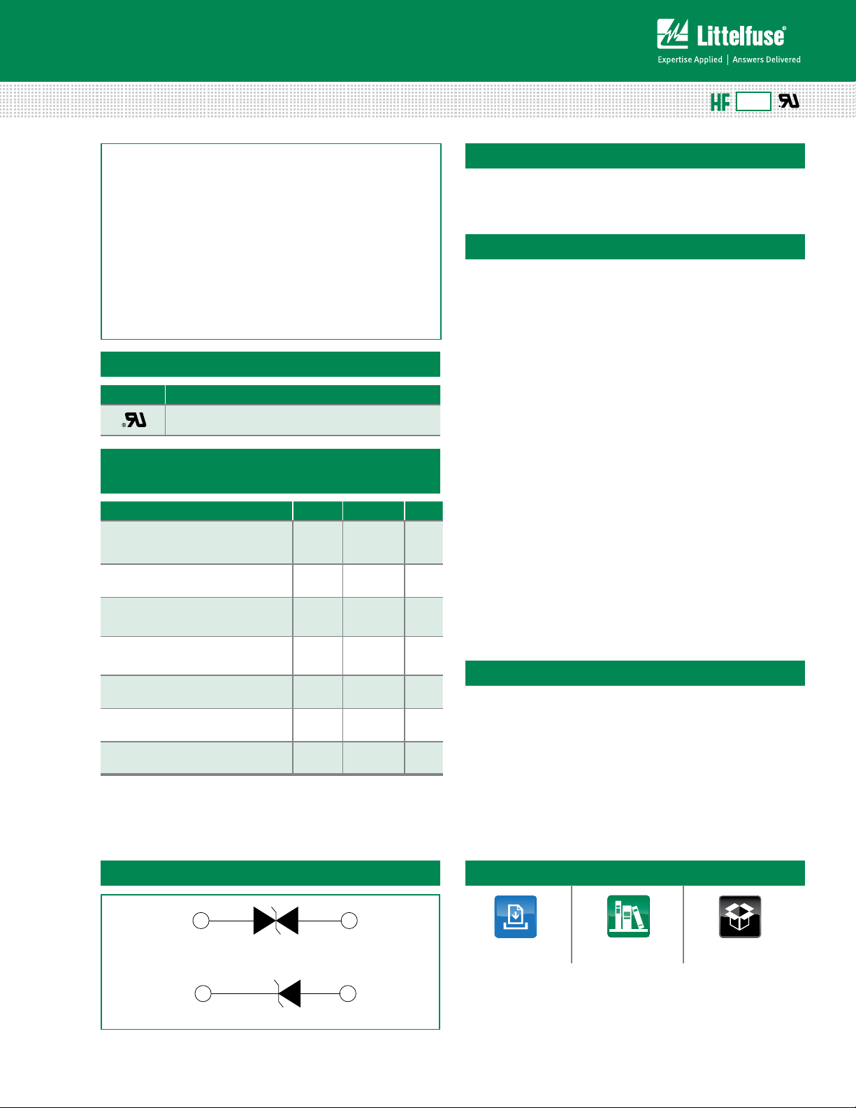
Functional Diagram
Bi-directional
Cathode
Uni-directional
© 2014 Littelfuse, Inc.
Specifications are subject to change without notice.
Revised: 01/24/14
Anode
Additional Information
Datasheet
Resources
Samples
Page 2

Transient Voltage Suppression Diodes
Axial Leaded – 600W > P6KE series
Electrical Characteristics (T
Part
Number
(Uni)
P6KE6.8A P6KE6.8CA 5.80 6.45 7. 1 4 10 10.5 58.1 1000 X
P6KE7.5A P6KE7.5CA 6.40 7. 13 7.88 10 11. 3 54.0 500 X
P6KE8.2A P6KE8.2CA 7.02 7.79 8.61 10 12.1 50.4 200 X
P6KE9.1A P6KE9.1CA 7.78 8.65 9.55 1 13.4 45.5 50 X
P6KE10A P6KE10CA 8.55 9.50 10.50 1 14.5 42.1 10 X
P6KE11A P6KE11CA 9.40 10.50 11.60 1 15.6 39.1 5 X
P6KE12A P6KE12CA 10.20 11.40 12.60 1 16.7 36.5 5 X
P6KE13A P6KE13CA 11. 10 12.40 13.70 1 18.2 33.5 1 X
P6KE15A P6KE15CA 12.80 14.30 15.80 1 21.2 28.8 1 X
P6KE16A P6KE16CA 13.60 15.20 16.80 1 22.5 27.1 1 X
P6KE18A P6KE18CA 15.30 1 7. 10 18.90 1 25.2 24.2 1 X
P6KE20A P6KE20CA 1 7. 10 19.00 21.00 1 27.7 22.0 1 X
P6KE22A P6KE22CA 18.80 20.90 23.10 1 30.6 19.9 1 X
P6KE24A P6KE24CA 20.50 22.80 25.20 1 33.2 18.4 1 X
P6KE27A P6KE27CA 23.10 25.70 28.40 1 37.5 16.3 1 X
P6KE30A P6KE30CA 25.60 28.50 31.50 1 41.4 14.7 1 X
P6KE33A P6KE33CA 28.20 31.40 34.70 1 45.7 13.3 1 X
P6KE36A P6KE36CA 30.80 34.20 37.80 1 49.9 12.2 1 X
P6KE39A P6KE39CA 33.30 37.10 41.00 1 53.9 11. 3 1 X
P6KE43A P6KE43CA 36.80 40.90 45.20 1 59.3 10.3 1 X
P6KE47A P6KE47CA 40.20 44.70 49.40 1 64.8 9.4 1 X
P6KE51A P6KE51CA 43.60 48.50 53.60 1 70.1 8.7 1 X
P6KE56A P6KE56CA 47.80 53.20 58.80 1 77.0 7. 9 1 X
P6KE62A P6KE62CA 53.00 58.90 65.10 1 85.0 7. 2 1 X
P6KE68A P6KE68CA 58.10 64.60 71.40 1 92.0 6.6 1 X
P6KE75A P6KE75CA 64.10 71.30 78.80 1 103.0 5.9 1 X
P6KE82A P6KE82CA 70.10 77.90 86.10 1 113.0 5.4 1 X
P6KE91A P6KE91CA 77.80 86.50 95.50 1 125.0 4.9 1 X
P6KE100A P6KE100CA 85.50 95.00 105.00 1 137.0 4.5 1 X
P6KE110A P6KE110CA 94.00 105.00 116.00 1 152.0 4.0 1 X
P6KE120A P6KE120CA 102.00 114.00 126.00 1 165.0 3.7 1 X
P6KE130A P6KE130CA 111. 0 0 124.00 137.00 1 179.0 3.4 1 X
P6KE150A P6KE150CA 128.00 143.00 158.00 1 207.0 2.9 1 X
P6KE160A P6KE160CA 136.00 152.00 168.00 1 219.0 2.8 1 X
P6KE170A P6KE170CA 145.00 162.00 179.00 1 234.0 2.6 1 X
P6KE180A P6KE180CA 154.00 171.00 189.00 1 246.0 2.5 1 X
P6KE200A P6KE200CA 171.00 190.00 210.00 1 274.0 2.2 1 X
P6KE220A P6KE220CA 185.00 209.00 231.00 1 328.0 1. 9 1 X
P6KE250A P6KE250CA 214.00 237.00 263.00 1 344.0 1. 8 1 X
P6KE300A P6KE300CA 256.00 285.00 315.00 1 414.0 1. 5
P6KE350A P6KE350CA 300.00 332.00 368.00 1 482.0 1. 3 1 X
P6KE400A P6KE400CA 342.00 380.00 420.00 1 548.0 1. 1 1 X
P6KE440A P6KE440CA 376.00 418.00 462.00 1 602.0 1. 0 1 X
P6KE480A P6KE480CA 408.00 456.00 504.00 1 658.0 0.9 1
P6KE510A P6KE510CA 434.00 485.00 535.00 1 698.0 0.9 1
P6KE530A P6KE530CA 477.00 503.50 556.50 1 725.0 0.8 1
P6KE540A P6KE540CA 486.00 513.00 567.00 1 740.0 0.8 1
P6KE550A P6KE550CA 495.00 522.50 577.50 1 760.0 0.8 1
P6KE600A P6KE600CA 512.00 570.00 630.00 1 828.0 0.75 1
For bidirectional type having VR of 10 volts and less, the IR limit is double.
For parts without A , the V
Part
Number
(Bi)
is ± 10% and VC is 5% higher than with A parts
BR
=25°C unless otherwise noted)
A
Reverse
Stand off
Voltage V
(Volts)
R
MIN MAX
Breakdown
Voltage V
BR
(Volts) @ I
Maximum
Peak
Pulse
Current Ipp
(A)
IT
Maximum
Clamping
Voltage
@ Ipp
V
C
(V)
T
Test
Current
(mA)
Maximum
Reverse
Leakage
IR@ VR
(µA)
1 X
Agency
Approval
Specifications are subject to change without notice.
© 2014 Littelfuse, Inc.
Revised: 01/24/14
Page 3

Transient Voltage Suppression Diodes
Voltage Transients
Time
Voltage Across TVS
Current Through TVS
Voltage or Current
0.1
1
10
100
0.001 0.01 0.11
P
PPM
-Peak Pulse Power (KW)
10
td-Pulse Width (ms)
Axial Leaded – 600W > P6KE series
I-V Curve Characteristics
Uni-directional
BR
V
Vc
VR
IR
VF
IT
V
Bi-directional
BR
V
Vc
VR
Ipp
P
Peak Pulse Power Dissipation -- Max power dissipation
PPM
V
Stand-off Voltage -- Maximum voltage that can be applied to the TVS without operation
R
V
Breakdown Voltage -- Maximum voltage that flows though the TVS at a specified test current (IT)
BR
V
Clamping Voltage -- Peak voltage measured across the suppressor at a specified Ippm (peak impulse current)
C
I
Reverse Leakage Current -- Current measured at V
R
V
Forward Voltage Drop for Uni-directional
F
Ratings and Characteristic Curves (T
Figure 1 - TVS Transients Clamping Waveform
R
=25°C unless otherwise noted)
A
Figure 2 - Peak Pulse Power Rating
Ipp
IT
IR
IR
IT
Ipp
VR
BR
V
V
Vc
P6KE Series
P6KE Series
© 2014 Littelfuse, Inc.
Specifications are subject to change without notice.
Revised: 01/24/14
continues on next page.
Page 4

Transient Voltage Suppression Diodes
100
175
Peak Pulse Power (P
) or Current (I
)
VBR - Re verse Breakdown Voltage (V)
Uni- directional V=0V
Bi-directional V=0V
Uni- directional @VR
Bi-directional @VR
Tj=25C
f=
Vs
Axial Leaded – 600W > P6KE series
Ratings and Characteristic Curves (T
=25°C unless otherwise noted) (Continued)
A
Figure 3 - Pulse Derating Curve
PP
80
60
PP
40
Derating in Percentage %
20
0
0255075 100 125 150
TA-Ambient temperature (ºC)
Figure 5 - Typical Junction Capacitance Uni-Directional
10000
1000
100
Cj (pF)
10
1.0MHz
ig=50mVp-p
1
1.010.0100.0 1000.0
Figure 4 - Pulse Waveform
150
RSM
100
50
- Peak Pulse Current, % I
PPM
I
0
tr=10µsec
Peak Value
I
PPM
t
d
0
1.0 2.0 3.0 4.0
Half Value
I
I
PPM
( )
TJ=25°C
Pulse Width(td) is defined
as the point where the peak
current decays to 50% of I
PPM
2
10/1000µsec. Waveform
as defined by R.E.A
t-Time (ms)
Figure 6 - Steady State Power Derating Curve
6
5
4
3
2
L = 0.375” (9.5mm)
Lead Lengths
1
Steady State Power Di ssipation (W)
0
0255075 100 125 150 175 200
TL-Lead Temperature (ºC)
PPM
Figure 7 - Maximum Non-Repetitive Forward Surge
Current
120
100
80
60
(A)
40
- Peak Forward Surge Current
20
FSM
I
0
110 100
Number of Cycles at 60 Hz
Specifications are subject to change without notice.
© 2014 Littelfuse, Inc.
Revised: 01/24/14
Page 5

Transient Voltage Suppression Diodes
Cathode Band
Axial Leaded – 600W > P6KE series
Soldering Parameters
Reflow Condition Lead–free assembly
Pre Heat
- Temperature Min (T
- Temperature Max (T
) 150°C
s(min)
) 200°C
s(max)
- Time (min to max) (ts) 60 – 180 secs
Average ramp up rate (Liquidus Temp
(T
) to peak
L
to TL - Ramp-up Rate 3°C/second max
T
S(max)
Reflow
- Temperature (TL) (Liquidus) 217°C
- Time (min to max) (ts) 60 – 150 seconds
Peak Temperature (TP) 260
Time within 5°C of actual peak
Temperature (t
)
p
3°C/second max
+0/-5
°C
20 – 40 seconds
Ramp-down Rate 6°C/second max
Time 25°C to peak Temperature (T
) 8 minutes Max.
P
Do not exceed 280°C
Physical Specifications
Weight 0.015oz., 0.4g
Case
JEDEC DO-204AC (DO-15) molded
plastic body over passivated junction.
t
T
P
Ramp-up Critical Zone
T
L
T
s(max)
T
s(min)
Temperature (T)
25˚C
t
s
Preheat
t 25˚C to Peak
Time (t)
p
Flow/Wave Soldering (Solder Dipping)
Peak Temperature : 265OC
Dipping Time : 10 seconds
Soldering : 1 time
Environmental Specifications
High Temp. Storage JESD22-A103
HTRB JESD22-A108
T
T
to
L
t
L
P
Ramp-down
Polarity
Terminal
Dimensions
A
Color band denotes the cathode except
Bipolar.
Matte Tin axial leads, solderable per
JESD22-B102.
(for Uni-directional products only)
D
B
DO-204AC (DO-15)
Temperature Cycling JESD22-A104
H3TRB JESD22-A101
RSH JESD22-B106
Dimensions
C
A
A 1.000 - 25.40 -
B 0.230 0.300 5.80 7.60
Inches Millimeters
Min Max Min Max
C 0.022 0.034 0.56 0.86
D 0.104 0.140 2.60 3.60
© 2014 Littelfuse, Inc.
Specifications are subject to change without notice.
Revised: 01/24/14
Page 6

Transient Voltage Suppression Diodes
OPTION CODE:
BLANK Reel Tape
-B Bulk Packaging
SERIES CODE
P6KE
xxx XX
X
TYPE CODE:
A Uni-Directional (5%
V
BR
Voltage Tolerance)
CA Bi-Directional (5%
V
BR
Voltage Tolerance)
V
BR
VOLTA GE CODE
(Refer to the Electrical Characteristics table)
Trace Code Marking
Littelfuse Logo
R
Axial Leaded – 600W > P6KE series
Part Numbering System
Part Marking System
Cathode Band
(for uni-directional
products only)
YYWW
F
P6KEXXX
YY:Year Code
WW: Week Code
Product Type
Packaging
Part Number Component Package Quantity Packaging Option Packaging Specification
P6KExxxXX DO-204AC 4000 Tape & Reel EIA STD RS-296
P6KExxxXX-B DO-204AC 1000 BULK Littelfuse Spec.
Tape and Reel Specification
2.56
(65.0)
0.197+/-0.020
(5.0+/- 0.5)
13.0
(330.2)
3.0
(76.2)
0.68
(17. 27)
2.75
(69.85)
ecess Depth Max. 0.75 (19.05)
Off Center
either side
0.028(0.7)
0.047
(1.2)
Dimensions are in
inches/mm
Direction of Feed
2.063+0.079/-0.039
(53.0+2.0/-1.0)
0.236
(6.0)
Specifications are subject to change without notice.
© 2014 Littelfuse, Inc.
Revised: 01/24/14
 Loading...