

Page 1
®
SIDACtor
Protection Thyristors
SLIC Protection
Battrax® Series - Single Port Negative - MS-013
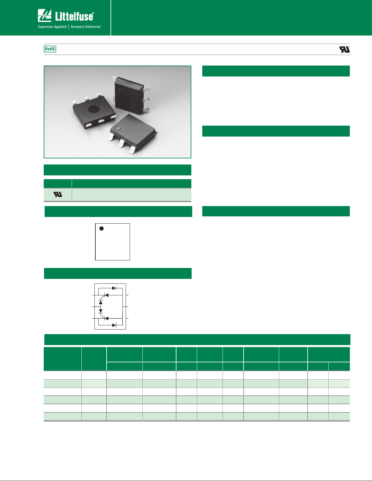
Description
The Battrax
overvoltage protection devices for SLIC applications.
The Single Port Negative Battrax Series provides a
programmable device that is referenced to a negative
voltage souce while internal diodes provide protection
from positive surge events.
Features and Benefits
®
series offers programmable SIDACtor®
Agency Approvals
Agency Agency File Number
E133083
Pinout Designation
1
2
3
Schematic Symbol
(T)
1
2
(-V
)
REF
(R)
3
6
5
4
6
(No Connect)
(G)
5
(No Connect)
4
• Low voltage overshoot
• Low on-state voltage
• Does not degrade with
use
• Fails short circuit when
surged in excess of
ratings
Applicable Global Standards
• TIA-968-A
• TIA-968-B
• ITU K.20/21 Enhanced
Level
• ITU K.20/21 Basic Level
• GR 1089 Inter-building
• Single-port protection
• Gate triggered tracking
device
• Integrated diodes for
positive voltage
• GR 1089 Intra-building
• IEC 61000-4-5
• YD/T 1082
• YD/T 993
• YD/T 950
Electrical Characteristics
V
DRM
@l
Part Number Marking
DRM
=5µA
V min V max mA min mA max A max V max V max pF min pF max
B1101UALxx B1101UA I-V
B1161UALxx B1161UA I-V
B1201UALxx B1201UA I-V
B1101UCLxx B1101UC I-V
B1161UCLxx B1161UC I-V
B1201UCLxx B1201UC I-V
Notes:
- Absolute maximum ratings measured at TA= 25ºC (unless otherwise noted).
- Devices are uni-directional
- All electrical characteristics shown are defined from Tip (pin 1) to Ground (pin 5), and Ring
(pin 3) to Ground (pin 5)
© 2011 Littelfuse, Inc.
Specifications are subject to change without notice.
Please refer to www.littelfuse.com for current information.
I + I-1.2VI I-V
REF
I + I-1.2VI I-V
REF
I + I-1.2VI I-V
REF
I + I-1.2VI I-V
REF
I + I-1.2VI I-V
REF
I + I-1.2VI I-V
REF
V
S
@100V/µs
I + I-10VI 100 100 2.2 4 5 30 200
REF
I + I-10VI 160 10 0 2.2 4 5 30 200
REF
I + I-10VI 200 100 2.2 4 5 30 200
REF
I + I-10VI 100 100 2.2 4 5 30 200
REF
I + I-10VI 160 10 0 2.2 4 5 30 200
REF
I + I-10VI 200 100 2.2 4 5 30 200
REF
I
H
Revised: September 30, 2011
V
I
S
- V
Max Value for the negative Battrax is -200 V.
REF
- XX = Part Number Suffix: ‘TP’ (Tube Pack) or ‘RP’ (Reel Pack).
* Off-state capacitance (C
at 1 MHz with a 2V bias.
118
I
T
T
@IT=2.2 Amps
) is measured across pins 1 & 5 and 3 & 5
O
V
F
Capacitance*
Page 2
®
50
100
0
t
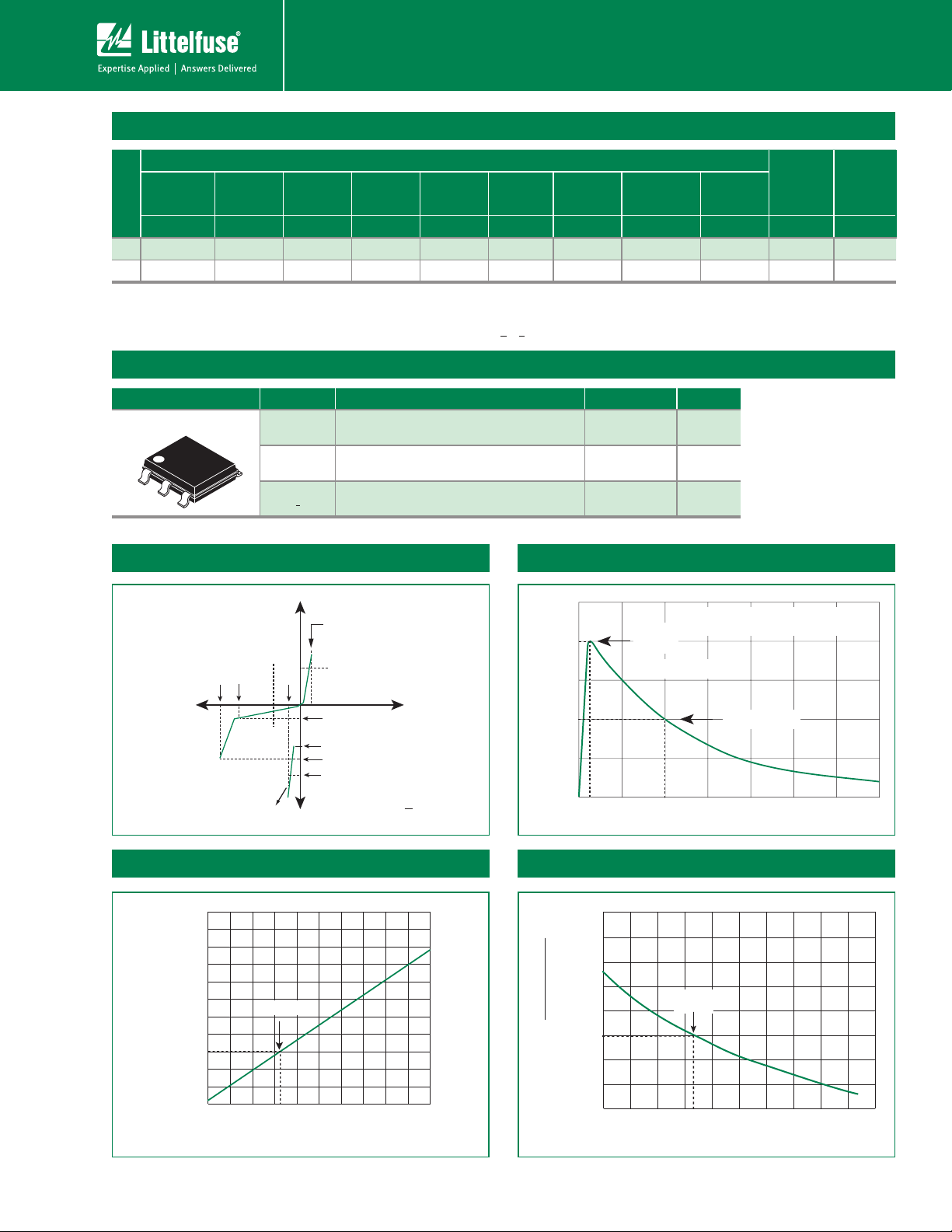
r
t
d
0
Peak
Value
Half Value
t – Time (µs)
I
PP
– Peak Pulse Current – %I
PP
tr = rise time to peak value
t
d
= decay time to half value
Waveform = t
r
x t
d
25°C
Case Temperature (TC) - ºC
2.0
1.8
1.6
1.4
1.2
1.0
0.8
0.6
0.4
-40 -20 020406080100 120140 160
Ratio of
I
H
I
H
(T
C
= 25ºC)
-8
-40 -20 020406080100 120140 160
-6
-4
0
2
4
6
8
10
12
14
Junction Temperature (TJ) – °C
Percent of V
S
Change – %
25 °C
SIDACtor
Protection Thyristors
SLIC Protection
Surge Ratings
I
PP
Series
0.2x310
0.5x700
1
2
2x10
2x10
1
2
8x20
1.2x50
1
2
10x160
10x160
1
2
10x560
10x560
1
2
5x320
9x720
1
2
10x360
10x360
1
2
10x10 00
10x10 00
1
2
5x310
10x700
A min A min A min A min A min A min A min A min A min A min A/µs max
A 20 150 150 90 50 75 75 45 75 20 500
C 50 500 400 200 150 200 175 10 0 200 50 500
Notes:
1 Current waveform in µs
2 Volt age waveform in µs
- Peak pulse current rating (IPP) is repetitive and guaranteed for the life of the product.
- IPP ratings applicable over temperature range of -40ºC to +85ºC (IPP rating assumes V
- The device must initially be in thermal equilibrium with -40°C < TJ < +150°C
equals +/- 48 V)
REF
Thermal Considerations
Package Symbol Parameter Value Unit
Modified MS-013
1
2
6
3
5
4
T
T
R
0JA
Operating Junction Temperature Range -40 to +125 °C
J
Storage Temperature Range -65 to +150 °C
S
Thermal Resistance: Junction to Ambient 60 °C/W
1
2
I
TSM
50/60 Hz
di/dt
V-I Characteristics tr x td Pulse Waveform
V
-V
Normalized VS Change vs. Junction Temperature
© 2011 Littelfuse, Inc.
Specifications are subject to change without notice.
Please refer to www.littelfuse.com for current information.
+I
V
V
REF
V
DRM
S
V
I
PP
I
F
T
I
DRM
I
H
I
S
I
T
PIN 5 CONNECTED TO GROUND
Pin 1-2:
PIN 2 CONNECTED TO V
PIN 2 CONNECTED TO GROUND
PIN 3 CONNECTED TO V
-I
+V
REF
REF
Normalized DC Holding Current vs. Case Temperature
119
Revised: September 30, 2011
Page 3

Time
Temperature
T
P
T
L
T
S(max)
T
S(min)
25
t
P
t
L
t
S
time to peak temperature
(t 25ºC to peak)
Ramp-down
Ramp-up
Preheat
Critical Zone
T
L
to T
P
Figure 1
Soldering Parameters
MS-013 Part Marking Drawing_2009-03-05.eps
SIDACtor
®
SLIC Protection
Protection Thyristors
Reflow Condition
Pre Heat
- Temperature Min (T
- Temperature Max (T
- Time (Min to Max) (ts)
s(min)
s(max)
)
)
Average ramp up rate (Liquidus Temp (T
to peak)
to TL - Ramp-up Rate
T
S(max)
Reflow
- Temperature (TL) (Liquidus)
- Temperature (tL)
Pb-Free assembly
(see Fig. 1)
+150°C
+200°C
60-180 secs.
)
L
3°C/sec. Max.
3°C/sec. Max.
+217°C
60-150 secs.
Peak Temp (TP) +260(+0/-5)°C
Time within 5°C of actual Peak Temp (t
)
p
30 secs. Max.
Ramp-down Rate 6°C/sec. Max.
Time 25°C to Peak Temp (T
)
P
8 min. Max.
Do not exceed +260°C
Physical Specifications
Lead Material Copper Alloy
Terminal Finish 100% Matte-Tin Plated
Body Material
UL recognized epoxy meeting flammability
classification 94V-0
Environmental Specifications
High Temp Voltage
Blocking
Temp Cycling
Biased Temp &
Humidity
High Temp Storage
Low Temp Storage -65°C, 1008 hrs.
Thermal Shock
Autoclave (Pressure
Cooker Test)
Resistance to Solder
Heat
Moisture Sensitivity
Level
80% Rated V
+150°C, 504 or 1008 hrs. MIL-STD-750 (Method
1040) JEDEC, JESD22-A-101
-65°C to +150°C, 15 min. dwell, 10 up to 100
cycles. MIL-STD-750 (Method 1051) EIA/JEDEC,
JESD22-A104
52 V
JEDEC, JESD22-A-101
+150°C 1008 hrs. MIL-STD-750 (Method 1031)
JEDEC, JESD22-A-101
0°C to +100°C, 5 min. dwell, 10 sec. transfer,
10 cycles. MIL-STD-750 (Method 1056) JEDEC,
JESD22-A-106
+121°C, 100%RH, 2atm, 24 up to 168 hrs. EIA/
JEDEC, JESD22-A-102
+260°C, 30 secs. MIL-STD-750 (Method 2031)
85%RH, +85°C, 168 hrs., 3 reflow cycles
(+260°C Peak). JEDEC-J-STD-020, Level 1
REF
(+85°C) 85%RH, 504 up to 1008 hrs. EIA/
DC
Max. (V
Peak ) +125°C or
DC
Part Numbering
TYPE
B1: Negative Battrax SIDACtor
HOLDING CURRENT
10: 10 0 mA 16: 160 mA
20: 200 mA
CONSTRUCTION VARIABLE
© 2011 Littelfuse, Inc.
Specifications are subject to change without notice.
Please refer to www.littelfuse.com for current information.
B1
Part Marking
xx
1
UxL
xx
PACKING OPTIONS
RP: Reel Pack
TP: Tube Pack
RoHS COMPLIANT
RATING
I
PP
PACKAGE TYPE
120
Revised: September 30, 2011
XXXXXXX
XXXXX
Part Marking Code
(Refer to Electrical Characteristics Table)
Date Code
Page 4

.157
Dimensions — MS-013
SIDACtor
®
SLIC Protection
Protection Thyristors
0.065
(1.65)
0.460
(11.68)
H
MIN Length
Dimension are in inches
(and millimeters).
Burr Side
4º
K
of Flat
0.059
(1.50)
J
G
F
7º TYP
E
7º TYP
Mold Split
Line
BSC*
7º TYP
Pad Outline
0.138
(3.50)
A
C
D
A
A
7º TYP
B
Packing Options
Package Type Description Quantity Added Suffix
Modified MS-013 6-pin
Tape and Reel Pack
U
Modified MS-013 6-pin
Tube Pack
150 0 RP EIA-481-D
500
(50 per tube)
TP N/A
96º
Detail A
Dimensions
Inches Millimeters
Min Max Min Max
A 0.360 0.364 9.14 9.25
B 0.352 0.356 8.94 9.04
C 0.400 0.412 10.16 10.46
D 0.043 0.045 1.09 1. 1 3
E 0.047 0.055 1. 1 9 1.40
F 0.293 0.297 7.44 7.54
G 0.289 0.293 7.34 7.44
H 0.089 0.093 2.26 2.36
J 0.041 0.049 1.04 1.24
K 0.020 0.51
BSC* 0.133 0.143 3.38 3.63
* BSC = Basic Spacing between Centers
Industry Standard
Tape and Reel Specification — MS-013
.630
(16.0)
.512 (13.0) Arbor
Hole Dia.
0.700
(17.8)
Tube Pack Specification — MS-013
.045
(1.14)
90˚
.165
(4.19)
Interior of the Tube
.150
(3.81)
.310
(7.87)
(13.34)
(4.0)
6
.225
(5.72)
.525
.472
(12.0)
.108
(2.74)
12.99
(330)
Message Location
.020 ± .005
(0.51 ± 0.13)
.110
(2.79)
A
Dimensions are in inches
(and millimeters)
Direction of Feed
WALL TYP.
A
.005
Dimensions are in inches
(and millimeters)
20.000 ± .030
(508.00 ± 0.76)
© 2011 Littelfuse, Inc.
Specifications are subject to change without notice.
Please refer to www.littelfuse.com for current information.
121
Revised: September 30, 2011
 Loading...