

Page 1
L01 Series
Teccor® brand Thyristors
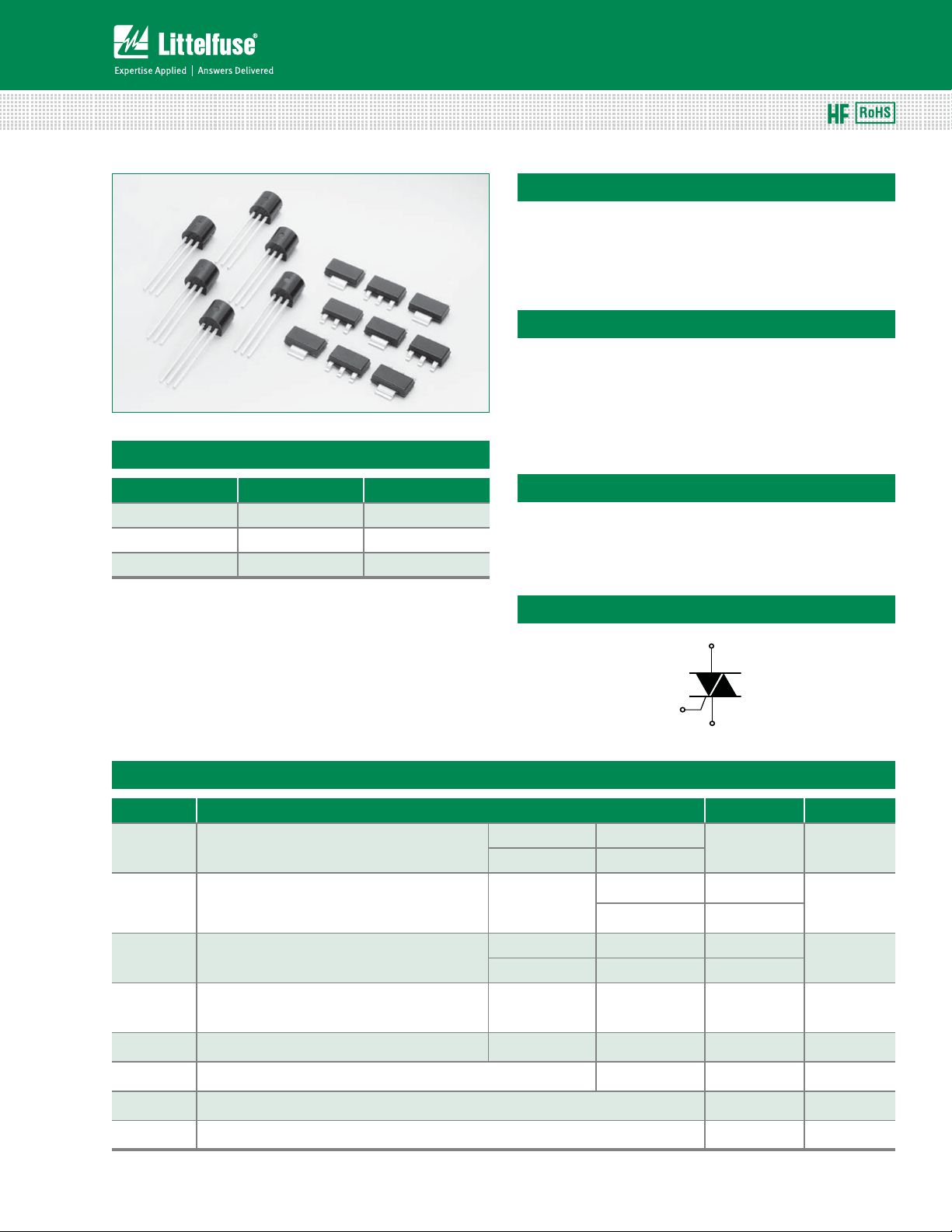
EV Series 1 Amp Sensitive Triacs
Description
New 1 Amp bi-directional solid state switch series offering
direct interface to microprocessor drivers in economical
TO-92 and surface mount packages. The die voltage
blocking junctions are glass-passivated to ensure long term
reliability and parametric stability.
Features
Main Features
Symbol Value Unit
I
T(RMS)
V
DRM/VRRM
I
GT
1A
400 to 800 V
3 to 10 mA
Absolute Maximum Ratings
t3P)4DPNQMJBOUBOE
Halogen-Free
t#MPDLJOHWPMUBHF7
DRM
capability — up to 800V
t4UBUJDEWEU7PMUT
μsec
)
t5ISVIPMFBOETVSGBDF
mount packages
t4VSHFDBQBCJMJUZ
10Amps
Applications
The L01 EV Series is especially designed for white goods
applications such as valve controls in washing machines as
well as replacement of mechanical and hybrid relays where
long life is required.
Schematic Symbol
MT2
G
MT1
Symbol Parameter Value Unit
I
T(RMS)
I
TSM
2
I
tI
Non repetitive surge peak on-state current
RMS on-state current
(full sine wave)
(Single cycle, TJ initial = 25°C)
2
t Value for fusing
di/dt Critical rate of rise of on-state current I
I
GTM
P
G(AV)
T
stg
T
J
L01 Series
Storage junction temperature range -40 to 150 °C
Operating junction temperature range -40 to 125 °C
Peak gate current tp = 10 μs
Average gate power dissipation
= 2 x I
G
TO-92 T
SOT-223 T
TO-92
SOT-223
tp = 10 ms F = 50 Hz 0.50
= 8.3 ms F = 60 Hz 0.59
t
p
GT
TO-92
SOT-223
45
= 50°C
C
= 90°C
L
1.0A A
F = 50 Hz 10
F = 60 Hz 12
= 125°C
T
J
T
= 125°C
J
T
= 125°C
J
Specifications are subject to change without notice.
20 A/μs
1A
0.1 W
A
A2s
©2013 Littelfuse, Inc
Revised: 09/23/13
Page 2

Teccor® brand Thyristors
EV Series 1 Amp Sensitive Triacs
Electrical Characteristics (T
Symbol Description
I
GT
V
GT
I
H
dv/dt
DC Gate Trigger Current
DC Gate Trigger Voltage ALL MAX. — 1.3 — V
Holding Current Gate Open MAX. 7 10 10 mA
Critical Rate-of-Rise of
Off-State Voltage
= 25°C, unless otherwise specified)
J
Test
Conditions
Quadrant Limit
*o**o***
DRM
IV
= 12V
V
D
RL = 60
= 110°C
T
J
VD = V
Exponential Waveform
Value
L0103xy L0107xy L0109xy
MAX.
3
5
5
7
10
10
MIN. 10 20 50 V/μs
Gate Open
(dv/dt)c
Critical
Rate-of-Rise of
Commutating Voltage
(di/dt)c = 0.54A/ms
= 110°C
T
J
MIN. 0.5 1.0 2.0 V/μs
IG = 25mA
T
gt
Note: x = voltage, y = package
Turn-On Time
Static Characteristics (T
= 25°C, unless otherwise specified)
J
PW = 15μs
IT = 1.2A (pk)
MAX. 2.0 2.0 2.0 μs
Symbol Description Test Conditions Limit Value Unit
V
I
TM
DRM
Peak On-State Voltage ITM = 1.4A (pk) MAX 1.60 V
Off-State Current, Peak Repetitive
= V
V
D
= V
V
D
= 25°C
DRM TJ
= 125°C 500 μA
DRM TJ
MAX
5μA
Unit
mA
Thermal Resistances
Symbol Description Test Conditions Value Unit
R
th(j-c)
R
th(j-a)
1
60Hz AC resistive load condition, 100% conduction.
Junction to case (AC) IT = 1.0A
Junction to ambient IT = 1.0A
(RMS)
(RMS)
1
1
TO-92 50
SOT-223 23
TO-92 100
SOT-223 55
°C/W
°C/W
L01 Series
46
Specifications are subject to change without notice.
©2013 Littelfuse, Inc
Revised: 09/23/13
Page 3
Teccor® brand Thyristors
T
EV Series 1 Amp Sensitive Triacs
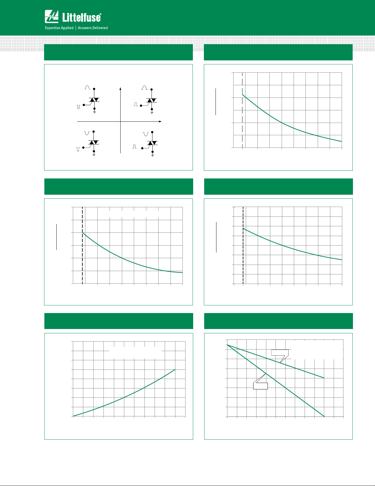
Figure 1: Definition of Quadrants
ALL POLARITIES ARE REFERENCED TO MT1
MT2 POSITIVE
(Positive Half Cycle)
MT2
(-)
I
GT
GATE
+
(+)
I
GT
GATE
MT2
MT1
I
REF
-
GT
(-)
I
GT
GATE
MT2
QII
QIII
QI
QIV
(+)
I
GT
GATE
REF
MT2
MT1
REF
-
MT2 NEGATIVE
(Negative Half Cycle)
REF
Figure 3: Normalized DC Holding Current
vs. Junction Temperature
3.0
INITIAL ON-STATE CURRENT = 100mA (DC)
+5
-15
+25
+45
+65
Junction Temperature (TJ)- ºC
H
I
= 25°C)
(T
I
Ratio of
2.5
2.0
J
1.5
H
1.0
0.5
0.0
-40
-55
MT1
MT1
+85
+ I
G
+105
+125
Figure 2: Normalized DC Gate Trigger Current for
All Quadrants vs. Junction Temperature
3.0
2.0
GT
= 25°C)
I
J
(T
GT
I
1.0
Ratio of
0.0
-15
-40
+25
+65
+105
Junction Temperature (TJ)- ºC
Figure 4: Normalized DC Gate Trigger Voltage for
All Quadrants vs. Junction Temperature
2.00
1.7 5
1.50
1.2 5
GT
= 25°C)
J
V
(T
1.0 0
GT
V
0.75
0.50
Ratio of
0.25
0.0
-40
-55
-15
+25
+5
+45
Junction Temperature (TJ)- °C
+65
+85
+105
+125
+125
Figure 5: Power Dissipation (Typical)
vs. RMS On-State Current
2.00
CURRENT WAVEFORM: Sinusoidal
LOAD: Resistive or Inductive
CONDUCTION ANGLE: 360°
0.3
0.4
0.6
0.5
RMS On-state Current [I
Average On-state Power Dissipation
L01 Series
1.7 5
1.50
1.2 5
] - Watts
1.0 0
D(DAV)
0.75
[P
0.50
0.25
0.0
0.1
0.0
0.2
T(RMS)
0.7
] - Amps
Figure 6: Maximum Allowable Case Temperature
vs. On-State Current
130
125
) - ºC
C
120
110
100
90
80
70
60
50
0.8
1.0
0.9
1.1
Maximum Allowable Case Temperature (T
0.0
0.1
TO-92
0.4
0.3
0.2
RMS On-state Current [I
47
CURRENT WAVEFORM: Sinusoidal
LOAD: Resistive or Inductive
CONDUCTION ANGLE: 360°
SOT-223
CASE TEMPERATURE: Measured as
shown on dimensional drawings
0.7
0.6
0.5
T(RMS)
Specifications are subject to change without notice.
0.8
] - Amps
0.9
1.0
©2013 Littelfuse, Inc
1.2
1.1
Revised: 09/23/13
Page 4

Teccor® brand Thyristors
Ramp-do
EV Series 1 Amp Sensitive Triacs
Figure 7: Surge Peak On-State Current vs. Number of Cycles
20
15
12
10
9
8
7
6
5
4
) – Amps.
TSM
(I
3
2
Peak Surge (Non-repetitive) On-State Current
1
12345 6 7 8 9 10 20 30 40 60 80 100 200 300 400 600 1 000
Surge Current Duration – Full Cycle
1 A Devices
Soldering Parameters
Reflow Condition 1Co'SFFBTTFNCMZ
- Temperature Min (T
Pre Heat
- Temperature Max (T
- Time (min to max) (ts) oTFDT
Average ramp up rate (Liquidus Temp)
(TL) to peak
T
to TL - Ramp-up Rate 5°C/second max
S(max)
Reflow
- Temperature (TL) (Liquidus) 217°C
- Time (min to max) (ts) oTFDPOET
Peak Temperature (TP) 260
Time within 5°C of actual peak
Temperature (tp)
Ramp-down Rate 5°C/second max
Time 25°C to peak Temperature (TP) 8 minutes Max.
Do not exceed 280°C
) 150°C
s(min)
) 200°C
s(max)
5°C/second max
+0/-5
°C
oTFDPOET
T
P
T
L
T
S(max)
Temperature
T
S(min)
25
Supply Frequency: 60Hz Sinusoidal
Load: Resistive
RMS On-State Current [I
Case Temperature
Notes:
1. Gate control may be lost during and immediately
following surge current interval.
2. Overload may not be repeated until junction
temperature has returned to steady-state rated value.
PreheatPreheat
t
S
time to peak temperature
]: Max Rated Value at Specific
T(RMS)
Ramp-upRamp-up
t
P
t
L
Ramp-down
Time
L01 Series
48
Specifications are subject to change without notice.
©2013 Littelfuse, Inc
Revised: 09/23/13
Page 5

Teccor® brand Thyristors
EV Series 1 Amp Sensitive Triacs
Physical Specifications Environmental Specifications
Terminal Finish 100% Matte Tin-plated.
Body Material
UL recognized epoxy meeting flammability
classification 94V-0.
Lead Material Copper Alloy
Design Considerations
Careful selection of the correct device for the application’s
operating parameters and environment will go a long way
toward extending the operating life of the Thyristor. Good
design practice should limit the maximum continuous
current through the main terminals to 75% of the device
rating. Other ways to ensure long life for a power discrete
semiconductor are proper heat sinking and selection of
voltage ratings for worst case conditions. Overheating,
overvoltage (including dv/dt), and surge currents are
the main killers of semiconductors. Correct mounting,
soldering, and forming of the leads also help protect
against component damage.
Test
AC Blocking
Specifications and Conditions
MIL-STD-750, M-1040, Cond A Applied
Peak AC voltage @ 125°C for 1008 hours
MIL-STD-750, M-1051,
Temperature Cycling
100 cycles; -40°C to +150°C; 15-min
dwell-time
Temperature/
Humidity
High Temp Storage
EIA / JEDEC, JESD22-A101
1008 hours; 320V - DC: 85°C; 85%
rel humidity
MIL-STD-750, M-1031,
1008 hours; 150°C
Low-Temp Storage 1008 hours; -40°C
MIL-STD-750, M-1056
Thermal Shock
10 cycles; 0°C to 100°C; 5-min dwelltime at each temperature; 10 sec (max)
transfer time between temperature
EIA / JEDEC, JESD22-A102
Autoclave
168 hours (121°C at 2 ATMs) and
100% R/H
Resistance to
Solder Heat
MIL-STD-750 Method 2031
Solderability ANSI/J-STD-002, category 3, Test A
Lead Bend
MIL-STD-750, M-2036 Cond E
Dimensions — TO-92 (E Package)
MT1
A
B
C
G
H
I
D
J
T MEASURING POINT
C
SEATING
PLANE
GATE
MT2
E
F
F
Dimensions
Inches Millimeters
Min Max Min Max
A 0.175 0.205 4.450 5.200
B 0.170 0.210 4.320 5.330
C 0.500 12.70
D 0.135 3.430
E 0.125 0.165 3.180 4.190
F 0.080 0.105 2.040 2.660
G 0.016 0.021 0.407 0.533
H 0.045 0.055 1.150 1.390
I 0.095 0.105 2.420 2.660
J 0.015 0.020 0.380 0.500
L01 Series
49
Specifications are subject to change without notice.
©2013 Littelfuse, Inc
Revised: 09/23/13
Page 6

Dimensions – SOT-223
Teccor® brand Thyristors
EV Series 1 Amp Sensitive Triacs
MT2
Gate
MT1
Pad Layout for SOT-223
3.3
(0.130”)
MT2
Dimensions
A 0.248 0.256 0.264 6.30 6.50 6.70
B 0.130 0.138 0.146 3.30 3.50 3.70
Inches Millimeters
Min Typ Max Min Typ Max
C — — 0.071 — — 1.80
1.5
(0.059”)
1.2
(0.047”)
(0.091”)
1.5
(0.059”)
(3x)
4.6
(0.181”)
Dimensions in Millimeters (Inches)
2.3
6.4
(0.252”)
D 0.001 — 0.004 0.02 — 0.10
E 0.114 0.118 0.124 2.90 3.00 3.15
F 0.024 0.027 0.034 0.60 0.70 0.85
G — 0.090 — — 2.30 —
H — 0.181 — — 4.60 —
I 0.264 0.276 0.287 6.70 7.00 7.30
J 0.009 0.010 0.014 0.24 0.26 0.35
K 10° MAX
Product Selector
Part Number Voltage
L0103DE 400 V 3 mA 5 mA TO-92
L0103ME 600 V 3 mA 5 mA TO-92
L0103NE 800 V 3 mA 5 mA TO-92
L0103DT 400 V 3 mA 5 mA SOT-223
L0103MT 600 V 3 mA 5 mA SOT-223
L0103NT 800 V 3 mA 5 mA SOT-223
L0107DE 400 V 5 mA 7 mA TO-92
L0107ME 600 V 5 mA 7 mA TO-92
L0107NE 800 V 5 mA 7 mA TO-92
L0107DT 400 V 5 mA 7 mA SOT-223
L0107MT 600 V 5 mA 7 mA SOT-233
L0107NT 800 V 5 mA 7 mA SOT-233
L0109DE 400 V 10 mA 10 mA TO-92
L0109ME 600 V 10 mA 10 mA TO-92
L0109NE 800 V 10 mA 10 mA TO-92
L0109DT 400 V 10 mA 10 mA SOT-223
L0109MT 600 V 10 mA 10 mA SOT-223
L0109NT 800 V 10 mA 10 mA SOT-223
Gate Sensitivity Quadrants
I II III IV
Package
L01 Series
50
Specifications are subject to change without notice.
©2013 Littelfuse, Inc
Revised: 09/23/13
Page 7

Teccor® brand Thyristors
EV Series 1 Amp Sensitive Triacs
Packing Options
Part Number Marking Weight Packing Mode Base Quantity
L01xxyE L01xxyE 0.170 g Bulk 2500
L01xxyEAP L01xxyE 0.170 g Ammo Pack 2000
L01xxyERP L01xxyE 0.170 g Tape & Reel 2000
L01xxyTRP L01xxyT 0.120 g Tape & Reel 1000
Note: xx = gate sensitivity, y = voltage
TO-92 (3-lead) Reel Pack (RP) Radial Leaded Specifications
Meets all EIA-468-C Standards
0.02 (0.5)
1.6
(41.0)
0.708
(18.0)
0.236
(6.0)
0.354
(9.0)
0.5
(12.7)
0.1 (2.54)
14.17(360.0)
MT1
0.2 (5.08)
MT2
Gate
0.098 (2.5) MAX
Flat up
0.157
(4.0)
1.26
(32.0)
DIA
1.97
(50.0)
TO-92 (3-lead) Ammo Pack (AP) Radial Leaded Specifications
Meets all EIA-468-C Standards
0.02 (0.5)
0.236
(6.0)
1.62
(41.2)
0.708
(18.0)
0.354
(9.0)
(12.7)
Direction of Feed
0.1 (2.54)
0.5
0.2 (5.08)
Direction of Feed
MT2
MT1
Gate
25 Devices per fold
0.098 (2.5) MAX
Flat down
1.85
(47.0)
0.157
(4.0)
Dimensions
are in inches
(and millimeters).
1.27
(32.2)
DIA
L01 Series
13.3
(338.0)
12.2
(310.0)
Dimensions
are in inches
1.85
(47.0)
51
(and millimeters).
Specifications are subject to change without notice.
©2013 Littelfuse, Inc
Revised: 09/23/13
Page 8

Teccor® brand Thyristors
EV Series 1 Amp Sensitive Triacs
SOT-223 Reel Pack (RP) Specifications
∅1.5 mm
1.7 5 mm
12 mm
13.4 mm
5.5 mm
Part Numbering System
13 mm Abor
Hole Diameter
4 mm
180 mm
8 mm
2 mm
MT1
Part Marking System
MT2
MT2
GATE
01
xxLx
TRIAC SERIES
CURRENT
01: 1A
SENSITIVITY & TYPE
03: 3, 3, 3, 5mA Triac
07: 5, 5, 5, 7mA Triac
09: 10, 10, 10, 10mA Triac
xx xx
PACKAGE TYPE
E: TO-92
T: SOT-223
VOLTAGE
D: 400V
M: 600V
N: 800V
PACKING TYPE
Blank: Bulk Pack
RP : Reel Pack (TO-92)
: Embossed Carrier Pack
(SOT-223)
AP : Ammo Pack (TO-92)
TO92
SOT223
Line1 = Littelfuse Part Number
Line2 = continuation…Littelfuse Part Number
Y = Last Digit of Calendar Year
M = Letter Month Code (A-L for Jan-Dec)
L = Location Code
DD = Calendar Date
L01 Series
52
Specifications are subject to change without notice.
©2013 Littelfuse, Inc
Revised: 09/23/13
 Loading...