

Page 1
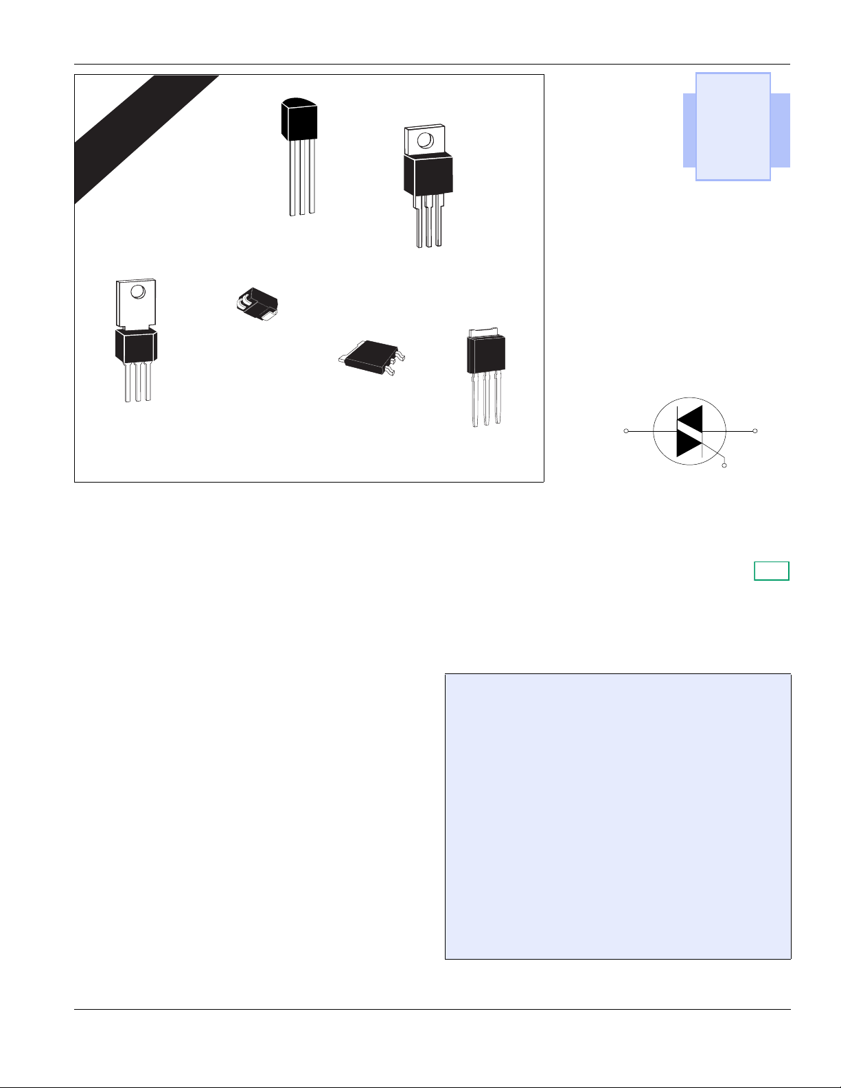
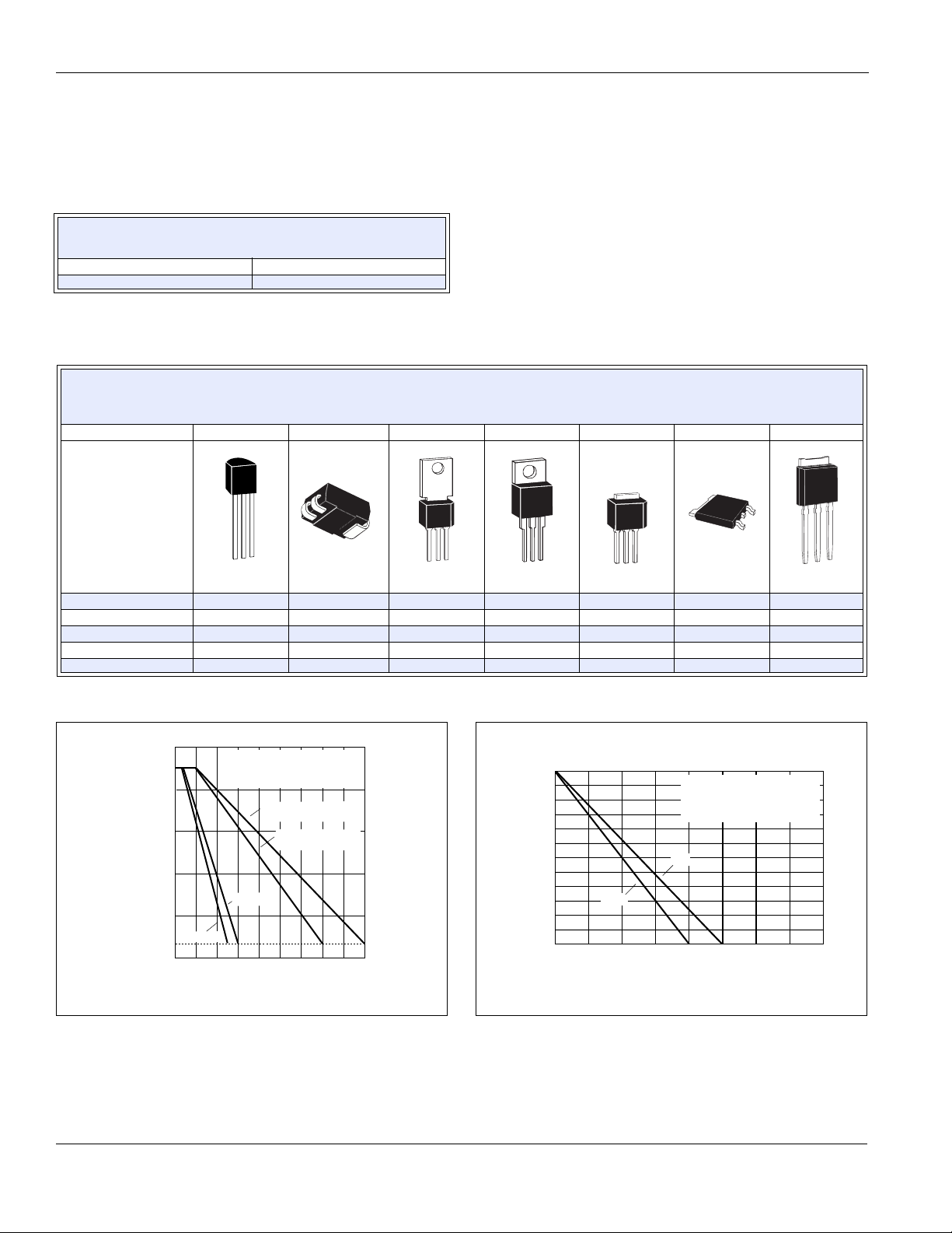
Selected Packages
*
File #E71639
U.L. RECOGNIZED
TO-202
E1
TO-92
*TO-220
Isolated
3-lead
Compak
TO-252
D-Pak
MT2 MT1
TO-251
V-Pak
G
Sensitive Triacs
E1
General Description
Teccor's line of sensitive gate triacs includes devices with current
capabilities through 8 A. Voltage ranges are available from 200 V
to 600 V. This line features devices with guaranteed gate control
in Quadrants II and IV as well as control in the commonly used
Quadrants I and III. Four-quadrant control devices require
sensitive gate triacs. They can be controlled by digital circuitry
where positive-only or negative-only pulses must control AC
current in both directions through the device. Note that triacs with
values in Quadrants II and IV will have lower dv/dt
low I
GT
characteristics.
The sensitive gate triac is a bidirectional AC switch and is gate
controlled for either polarity of main terminal voltage. It is used
primarily for AC switching and phase control applications such as
motor speed controls, temperature modulation controls, and
lighting controls.
The epoxy TO-92 and TO-220 configurations feature Teccor's
electrically-isolated construction where the case or mounting tab
is internally isolated from the semiconductor chip and lead
attachments. Non-isolated epoxy TO-202 packages are available
as well as TO-251 and surface mount TO-252 (D-Pak). Tapeand-reel capability and tube packing also are available. See
“Packing Options” section of this catalog.
All Teccor triacs have glass-passivated junctions. This glassing
process prevents migration of contaminants and ensures longterm device reliability with parameter stability.
RoH
(0.8 A to 8 A)
Variations of devices covered in this data sheet are available for
custom design applications. Consult factory for more information.
S
Features
•RoHS Compliant
• Electrically-isolated packages
• Glass-passivated junctions ensure long device
reliability and parameter stability
• Voltage capability — up to 600 V
• Surge capability — up to 80 A
• Four-quadrant gating guaranteed
Compak Sensitive Gate Triac
• Surface mount package — 0.8 A and 1 A series
• New small profile three-leaded Compak package
• Packaged in embossed carrier tape with 2,500
devices per reel
• Can replace SOT-223
©2004 Littelfuse, Inc. E1 - 1 http://www.littelfuse.com
Thyristor Product Catalog +1 972-580-7777
Page 2
Sensitive Triacs Data Sheets
I
T(RMS)
(11)
MT2
MT1
G
TO-92 Compak TO-220
Isolated Non-isolated
MT2
MT1
G
MT2
MT1
MT2
MT2
G
G
MT2
MT1
TO-252
D-Pak TO-202
MT1
MT2
MT2
G
MT1
TO-251
V-Pak
MAX See “Package Dimensions” section for variations. (12) MIN MAX MAX
L2X8E3 L2X3 200 3 3 3 3 0.01 0.1
L4X8E3 L4X3 400 3 3 3 3 0.01 0.1
L6X8E3 L6X3 600 3 3 3 3 0.01 0.1
L2X8E5 L2X5 200 5 5 5 5 0.01 0.1
L4X8E5 L4X5 400 5 5 5 5 0.01 0.1
0.8 A
L6X8E5 L6X5 600 5 5 5 5 0.01 0.1
L2X8E6 200 5 5 5 10 0.01 0.1
L4X8E6 400 5 5 5 10 0.01 0.1
L6X8E6 600 5 5 5 10 0.01 0.1
L2X8E8 200 10 10 10 20 0.01 0.1
L4X8E8 400 10 10 10 20 0.01 0.1
L6X8E8 600 10 10 10 20 0.01 0.1
L201E3 L2N3 200 33330.010.1
L401E3 L4N3 400 33330.010.1
L601E3 L6N3 600 33330.010.1
L201E5 L2N5 200 55550.010.1
L401E5 L4N5 400 55550.010.1
1A
L601E5 L6N5 600 55550.010.1
L201E6 200 5 5 5 10 0.01 0.1
L401E6 400 5 5 5 10 0.01 0.1
L601E6 600 5 5 5 10 0.01 0.1
L201E8 200 10101020 0.01 0.1
L401E8 400 10101020 0.01 0.1
L601E8 600 10101020 0.01 0.1
L2004L3 L2004D3 L2004F31 L2004V3 200 3 3 3 3 0.01 0.2
L4004L3 L4004D3 L4004F31 L4004V3 400 3 3 3 3 0.01 0.2
L6004L3 L6004D3 L6004F31 L6004V3 600 3 3 3 3 0.01 0.2
L2004L5 L2004D5 L2004F51 L2004V5 200 5 5 5 5 0.01 0.2
L4004L5 L4004D5 L4004F51 L4004V5 400 5 5 5 5 0.01 0.2
4A
L6004L5 L6004D5 L6004F51 L6004V5 600 5 5 5 5 0.01 0.2
L2004L6 L2004D6 L2004F61 L2004V6 200 5 5 5 10 0.01 0.2
L4004L6 L4004D6 L4004F61 L4004V6 400 5 5 5 10 0.01 0.2
L6004L6 L6004D6 L6004F61 L6004V6 600 5 5 5 10 0.01 0.2
L2004L8 L2004D8 L2004F81 L2004V8 200 10 10 10 20 0.01 0.2
L4004L8 L4004D8 L4004F81 L4004V8 400 10 10 10 20 0.01 0.2
L6004L8 L6004D8 L6004F81 L6004V8 600 10 10 10 20 0.01 0.2
MT2
V
DRM
(1)
G
I
GT
(3) (6) (9)
mAmps
Volts
QI QII QIII QIV
25 °C
See “General Notes” on page E1 - 4 and “Electrical Specification Notes” on page E1 - 5.
Part No.
T
C
I
DRM
(1) (14)
mAmps
=
TC =
110 °C
http://www.littelfuse.com E1 - 2 ©2004 Littelfuse, Inc.
+1 972-580-7777 Thyristor Product Catalog
Page 3

Data Sheets Sensitive Triacs
V
TM
(1) (4)
Volts
T
=
C
25 °C
MAX MAX MAX TYP TYP TYP
1.6 2 5 1 10 0.2 10/8.3 0.5 20 2.8 0.41 20
1.6 2 5 1 10 0.2 10/8.3 0.5 15 2.8 0.41 20
1.6 2 5 1 10 0.2 10/8.3 0.5 10 2.8 0.41 20
1.6 2 10 1 10 0.2 10/8.3 1 20 3 0.41 20
1.6 2 10 1 10 0.2 10/8.3 1 15 3 0.41 20
1.6 2 10 1 10 0.2 10/8.3 1 10 3 0.41 20
1.6 2 10 1 10 0.2 10/8.3 1 30 3 0.41 20
1.6 2 10 1 10 0.2 10/8.3 1 25 3 0.41 20
1.6 2 10 1 10 0.2 10/8.3 1 20 3 0.41 20
1.6 2 15 1 10 0.2 10/8.3 2 35 3.2 0.41 20
1.6 2 15 1 10 0.2 10/8.3 2 30 3.2 0.41 20
1.6 2 15 1 10 0.2 10/8.3 2 25 3.2 0.41 20
1.625110 0.220/16.70.5 202.81.6 20
1.625110 0.220/16.70.5 202.81.6 20
1.625110 0.220/16.70.5 102.81.6 20
1.6 2 10 1 10 0.2 20/16.7 1 20 3 1.6 20
1.6 2 10 1 10 0.2 20/16.7 1 20 3 1.6 20
1.6 2 10 1 10 0.2 20/16.7 1 10 3 1.6 20
1.6 2 10 1 10 0.2 20/16.7 1 30 3 1.6 20
1.6 2 10 1 10 0.2 20/16.7 1 30 3 1.6 20
1.6 2 10 1 10 0.2 20/16.7 1 20 3 1.6 20
1.6 2 15 1 10 0.2 20/16.7 1 35 3.2 1.6 20
1.6 2 15 1 10 0.2 20/16.7 1 35 3.2 1.6 20
1.6 2 15 1 10 0.2 20/16.7 1 25 3.2 1.6 20
1.6 2 5 1.2 15 0.3 40/33 0.5 25 2.8 6.6 50
1.6 2 5 1.2 15 0.3 40/33 0.5 25 2.8 6.6 50
1.6 2 5 1.2 15 0.3 40/33 0.5 15 2.8 6.6 50
1.6 2 10 1.2 15 0.3 40/33 1 25 3 6.6 50
1.6 2 10 1.2 15 0.3 40/33 1 25 3 6.6 50
1.6 2 10 1.2 15 0.3 40/33 1 15 3 6.6 50
1.6 2 10 1.2 15 0.3 40/33 1 30 3 6.6 50
1.6 2 10 1.2 15 0.3 40/33 1 30 3 6.6 50
1.6 2 10 1.2 15 0.3 40/33 1 20 3 6.6 50
1.6 2 15 1.2 15 0.3 40/33 2 35 3.2 6.6 50
1.6 2 15 1.2 15 0.3 40/33 2 35 3.2 6.6 50
1.6 2 15 1.2 15 0.3 40/33 2 25 3.2 6.6 50
V
GT
(2) (5) (15)
Volts
TC =
25 °C60/50Hz
I
H
(1) (7)
mAmps
I
GTM
(13)
Amps
P
GM
(13)
Watts Watts
P
G(AV)
I
TSM
(8) (10)
Amps
dv/dt(c) dv/dt
(1) (10)
Volts/µSec
(1)
Volts/µSec
TC =
100 °C
t
gt
(9)
µSec Amps
I2t di/dt
2
Sec Amps/µSec
See “General Notes” on page E1 - 4 and “Electrical Specification Notes” on page E1 - 5.
©2004 Littelfuse, Inc. E1 - 3 http://www.littelfuse.com
Thyristor Product Catalog +1 972-580-7777
Page 4
Sensitive Triacs Data Sheets
I
T(RMS)
(11)
MAX See “Package Dimensions” section for variations. (12) MIN MAX MAX
6A
8A
Isolated Non-isolated
MT2
MT2
G
MT1
MT2
TO-220
L2006L5 L2006D5 L2006V5 200 5555 0.02 0.5
L4006L5 L4006D5 L4006V5 400 5555 0.02 0.5
L6006L5 L6006D5 L6006V5 600 5555 0.02 0.5
L2006L6 L2006D6 L2006V6 200 5 5 5 10 0.02 0.5
L4006L6 L4006D6 L4006V6 400 5 5 5 10 0.02 0.5
L6006L6 L6006D6 L6006V6 600 5 5 5 10 0.02 0.5
L2006L8 L2006D8 L2006V8 200 10 10 10 20 0.02 0.5
L4006L8 L4006D8 L4006V8 400 10 10 10 20 0.02 0.5
L6006L8 L6006D8 L6006V8 600 10 10 10 20 0.02 0.5
L2008L6 L2008D6 L2008V6 200 5 5 5 10 0.02 0.5
L4008L6 L4008D6 L4008V6 400 5 5 5 10 0.02 0.5
L6008L6 L6008D6 L6008V6 600 5 5 5 10 0.02 0.5
L2008L8 L2008D8 L2008V8 200 10 10 10 20 0.02 0.5
L4008L8 L4008D8 L4008V8 400 10 10 10 20 0.02 0.5
L6008L8 L6008D8 L6008V8 600 10 10 10 20 0.02 0.5
MT1
TO-252
D-Pak
MT2
G
G
MT1
MT2
TO-251
V-P ak
V
Volts
DRM
(1)
QI QII QIII QIV T
I
GT
(3) (6)
mAmps
(1) (14)
mAmps
= 25 °C TC = 110 °C
C
Part No.
I
DRM
Specified Test Conditions
di/dt — Maximum rate-of-change of on-state current; IGT = 50 mA with
0.1
µs rise time
dv/dt — Critical rate-of-rise of off-state voltage at rated V
dv/dt(c) — Critical rate-of-rise of commutation voltage at rated V
and I
commutating di/dt = 0.54 rated I
T(RMS)
T(RMS)
unenergized
2
I
t — RMS surge (non-repetitive) on-state current for period of 8.3 ms
for fusing
I
— Peak off-state current, gate open; V
DRM
I
— DC gate trigger current in specific operating quadrants;
GT
V
= 12 V dc; RL = 60 Ω
D
I
— Peak gate trigger current
GTM
I
— Holding current gate open; initial on-state current = 100 mA dc
H
I
— RMS on-state current conduction angle of 360°
T(RMS)
I
— Peak one-cycle surge
TSM
P
— Average gate power dissipation
G(AV)
P
— Peak gate power dissipation; I
GM
GT
= max rated value
DRM
≤ I
GTM
tgt — Gate controlled turn-on time; IGT = 50 mA with 0.1 µs rise time
V
— Repetitive peak off-state/blocking voltage
DRM
V
— DC gate trigger voltage; VD = 12 V dc; RL = 60 Ω
GT
V
— Peak on-state voltage at max rated RMS current
TM
DRM
/ms; gate
gate open
DRM
General Notes
• All measurements are made with 60 Hz resistive load and at an
ambient temperature of +25 °C unless otherwise specified.
• Operating temperature range (T
devices and -40 °C to +110 °C for all other devices.
• Storage temperature range (T
devices, -40 °C to +150 °C for TO-202 devices, and -40 °C to
+125 °C for TO-220 devices.
• Lead solder temperature is a maximum of 230 °C for 10 seconds
maximum at a minimum of 1/16” (1.59 mm) from case.
• The case or lead temperature (T
dimensional outline drawings. See “Package Dimensions” section
of this catalog.
) is -65 °C to +110 °C for TO-92
J
) is -65 °C to +150 °C for TO-92
S
or TL) is measured as shown on
C
http://www.littelfuse.com E1 - 4 ©2004 Littelfuse, Inc.
+1 972-580-7777 Thyristor Product Catalog
Page 5
Data Sheets Sensitive Triacs
V
TM
(1) (4)
Volts
T
= 25 °C TC = 25 °C 60/50 Hz TC = 100 °C
C
MAX MAX MAX TYP TYP TYP
1.6 2 10 1.6 18 0.4 60/50 1 40 3 15 70
1.6 2 10 1.6 18 0.4 60/50 1 30 3 15 70
1.6 2 10 1.6 18 0.4 60/50 1 20 3 15 70
1.6 2 10 1.6 18 0.4 60/50 2 40 3 15 70
1.6 2 10 1.6 18 0.4 60/50 2 30 3 15 70
1.6 2 10 1.6 18 0.4 60/50 2 20 3 15 70
1.6 2 20 1.6 18 0.4 60/50 2 45 3.2 15 70
1.6 2 20 1.6 18 0.4 60/50 2 40 3.2 15 70
1.6 2 20 1.6 18 0.4 60/50 2 30 3.2 15 70
1.6 2 10 1.6 18 0.4 80/65 2 40 3 26.5 70
1.6 2 10 1.6 18 0.4 80/65 2 30 3 26.5 70
1.6 2 10 1.6 18 0.4 80/65 2 20 3 26.5 70
1.6 2 20 1.6 18 0.4 80/65 2 45 3.2 26.5 70
1.6 2 20 1.6 18 0.4 80/65 2 40 3.2 26.5 70
1.6 2 20 1.6 18 0.4 80/65 2 30 3.2 26.5 70
Electrical Specification Notes
(1) For either polarity of MT2 with reference to MT1 terminal
(2) For either polarity of gate voltage V
terminal
(3) See Gate Characteristics and Definition of Quadrants.
(4) See Figure E1.4 for i
(5) See Figure E1.6 for V
(6) See Figure E1.7 for I
(7) See Figure E1.5 for I
(8) See Figure E1.9 for surge rating and specific duration.
(9) See Figure E1.8 for t
(10) See Figure E1.2 and Figure E1.3 for maximum allowable case
temperature at maximum rated current.
(11) See Figure E1.1, Figure E1.2, and Figure E1.3 for T
I
T(RMS)
(12) See package outlines for lead form configurations. When ordering
special lead forming, add type number as suffix to part number.
(13) Pulse width ≤10 µs
or T
(14) T
C
(15) Minimum non-trigger V
V
GT
(2) (5) (15)
Volt s
I
H
(1) (7)
mAmps
versus vT.
T
versus TC.
GT
versus TC.
GT
versus TC.
H
versus IGT.
gt
I
GTM
(13)
Amps
.
= TJ for test conditions in off state
L
at 110 °C is 0.2 V.
GT
P
GM
(13)
Watts Watts
with reference to MT1
GT
P
or TC versus
A
G(AV)
I
TSM
(8) (10)
Amps
dv/dt(c) dv/dt
(1) (10)
Volt s/µSe c
(1)
Volt s/µSe c
t
gt
(9)
µSec Amps
I2t di/dt
2
Sec Amps/µSec
Gate Characteristics
Teccor triacs may be turned on between gate and MT1 terminals
in the following ways:
• In-phase signals (with standard AC line) using Quadrants I
and III
• Application of unipolar pulses (gate always positive or negative), using Quadrants II and III with negative gate pulses and
Quadrants I and IV with positive gate pulses
When maximum surge capability is required, pulses should be a
minimum of one magnitude above I
waveform (
≤1 µs rise time).
ALL POLARITIES ARE REFERENCED TO MT1
(-)
I
GT
GATE
IGT
-
(-)
I
GT
GATE
MT2 POSITIVE
(Positive Half Cycle)
MT2
MT1
REF
MT2
REF
QIII
MT1
MT2 NEGATIVE
(Negative Half Cycle)
rating with a steep rising
GT
+
(+)
I
GT
GATE
QII
QI
QIV
(+)
I
GT
GATE
-
MT2
REF
MT2
REF
Definition of Quadrants
MT1
MT1
+
I
GT
©2004 Littelfuse, Inc. E1 - 5 http://www.littelfuse.com
Thyristor Product Catalog +1 972-580-7777
Page 6
Sensitive Triacs Data Sheets
Electrical Isolation
Teccor’s isolated triac packages withstand a minimum high
potential test of 2500 V ac rms from leads to mounting tab over
the device's operating temperature range. The following isolation
table shows standard isolation ratings.
Electrical Isolation
from Leads to Mounting Tab
V AC RMS TO-220 *
2500 Standard
*UL Recognized File #E71639
Thermal Resistance (Steady State) Junction to Mounting Tab
and Junction to Ambient
R
[R
θJC
] °C/W (TYP)
θJA
Package Code ECFLF2DV
Typ e
TO-92
Plastic Compak
TO-202
Type 1
TO-220
Isolated
TO-202
Type 2
TO-252
D-Pak
TO-251
V-P ak
0.8 A 60 [135] 60 *
1 A 50 [95] 40 *
4A 3.5 [45] 3.6 [50] 6.0 [70] 3.5 6.0 [70]
6A 3.3 3.2 3.2
8A 2.8 2.7 2.7
* Mounted on 1 cm2 copper foil surface; two-ounce copper foil
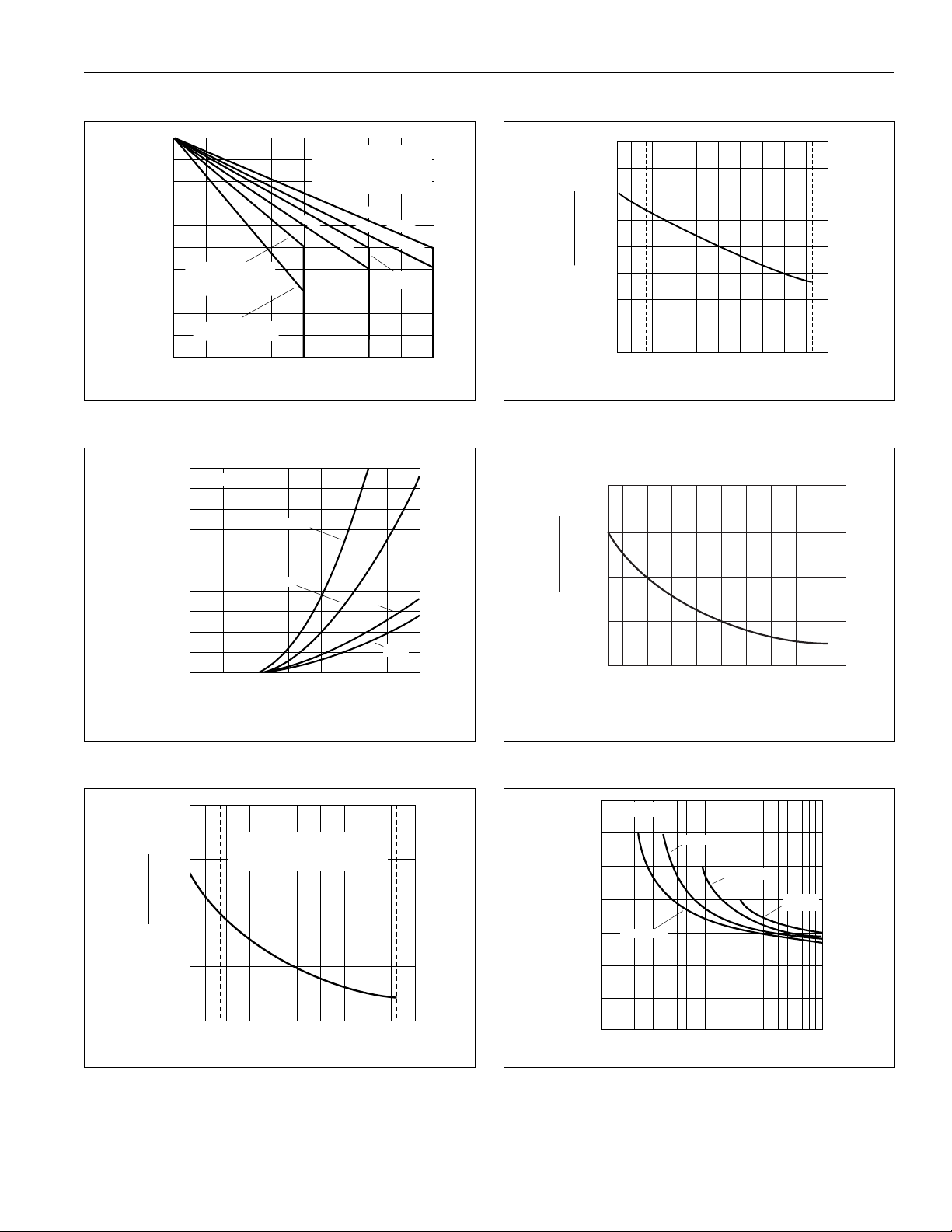
120
) - ˚C
A
T
100
80
60
40
25
20
Maximum Allowable Ambient Temperature (
0 0.2 0.4 0.6 0.8 1.0 1.2 1.4 1.6 1.8
CURRENT WAVEFORM: Sinusoidal
LOAD: Resistive or Inductive
CONDUCTION ANGLE: 360
FREE AIR RATING – NO HEATSINK
1 A TO-92
0.8 A TO-92
RMS On-State Current [I
˚
TO-220 and
TYPE 1 and 3 TO-202
TYPE 2 and 4 TO-202
and TO-251
] - Amps
T(RMS)
110
) – ˚C
C
100
90
80
70
60
50
0 0.2 0.4 0.6 0.8 1.0 1.2 1.4 1.6
Maximum Allowable Case Temperature (T
0.8 A
RMS On-State Current [I
CURRENT WAVEFORM: Sinusoidal
LOAD: Resistive or Inductive
CONDUCTION ANGLE: 360˚
CASE TEMPERATURE: Measured as
shown on Dimensional Drawings
1 A
] – Amps
T(RMS)
Figure E1.1 Maximum Allowable Ambient Temperature versus
On-state Current
Figure E1.2 Maximum Allowable Case Temperature versus
On-state Current (0.8 A and 1 A)
http://www.littelfuse.com E1 - 6 ©2004 Littelfuse, Inc.
+1 972-580-7777 Thyristor Product Catalog
Page 7
Data Sheets Sensitive Triacs
110
- ˚C
)
105
C
T
(
100
95
90
85
80
4 A TYPE 1 and 3 TO-202
4 A TO-220 (Isolated)
4 A TO-252
75
70
4 A TYPE 2 and 4 TO-202
65
4 A TO-251
Maximum Allowable Case Temperature
60
01 23 4 5 67 8
RMS On-State Current [I
CURRENT WAVEFORM: Sinusoidal
LOAD: Resistive or Inductive
CONDUCTION ANGLE: 360˚
CASE TEMPERATURE: Measured as
shown on Dimensional Drawings
6 A TO-220 (Isolated)
8 A TO-251 and TO-252
8 A TO-220 (Isolated)
T(RMS)
6 A TO-251
6 A TO-252
] - Amps
Figure E1.3 Maximum Allowable Case Temperature versus
On-state Current (4 A, 6 A, and 8 A)
20
TC = 25 ˚C
18
16
14
) - Amps
12
T
10
8
6
4
On-state Current (i
Positive or Negative Instantaneous
2
0
0 0.5 0.8 1.0 1.2 1.4 1.6 1.8
6 A and 8 A
4 A
1 A
Positive or Negative Instantaneous
On-state Voltage (v
) - Volts
T
0.8 A
2.0
1.5
= 25 ˚C)
GT
C
V
(T
1.0
GT
V
.5
Ratio of
0
-65 -40 -15 +65 +110+125+25
Case Temperature (
) - ˚C
T
C
Figure E1.6 Normalized DC Gate Trigger Voltage for All Quadrants
versus Case Temperature
4.0
3.0
= 25 ˚C)
GT
I
C
(T
2.0
GT
I
1.0
Ratio of
0
-65 -40 -15 +65 +110+125+25
Case Temperature (TC) - ˚C
Figure E1.4 On-state Current versus On-state Voltage (Typical)
Figure E1.7 Normalized DC Gate Trigger Current for All Quadrants
versus Case Temperature
4.0
INITIAL ON-STATE CURRENT
= 100 mA (DC) 0.8 - 4 A Devices
= 200 mA (DC) 6 - 8 A Devices
-40 -15 +25 +65
Case Temperature (
T
) - ˚C
C
+110
+125
H
I
3.0
C)
˚
= 25
C
2.0
(T
H
I
Ratio of
1.0
0
-65
Figure E1.5 Normalized DC Holding Current versus Case Temperature
Figure E1.8 Turn-on Time versus Gate Trigger Current (Typical)
7.0
TC = 25 ˚C
6.0
5.0
) - µSec
gt
4.0
3.0
IGT = 3 mA MAX
Turn-On Time (t
2.0
1.0
0
123465 8 10 20 30 40 60 80 100
IGT = 5 mA MAX
IGT = 10 mA MAX
DC Gate Trigger Current (IGT) - mA
IGT = 20 mA
MAX
©2004 Littelfuse, Inc. E1 - 7 http://www.littelfuse.com
Thyristor Product Catalog +1 972-580-7777
Page 8

Sensitive Triacs Data Sheets
200
150
100
SUPPLY FREQUENCY: 60 Hz Sinusoidal
LOAD: Resistive
RMS On-state Current: [I
Rated Value at Specified Case Temperature
80
T(RMS)
60
40
) – Amps
30
TSM
20
10
8
6
4
Peak Surge (Non-Repetitive)
3
On-State Current (I
2
1
1 2436810204030 60 100 200 400 600 1000
]: Maximum
NOTES:
1) Gate control may be lost during
and immediately following surge
current interval.
2) Overload may not be repeated until
junction temperature has returned
to steady-state rated value.
8 A
6 A
4 A
1 A
0.8 A
Surge Current Duration – Full Cycles
Figure E1.9 Peak Surge Current versus Surge Current Duration
CURRENT WAVEFORM: Sinusoidal
LOAD: Resistive or Inductive
1.5
CONDUCTION ANGLE: 360˚
1.0
] – Watts
D(AV)
0.5
[P
Average On-state Power Dissipation
Figure E1.10 Power Dissipation (Typical) versus RMS On-state Current
(0.8 A and 1 A)
0.8 A
0
0 0.25 0.50 0.75 1.0 1.25 1.5
RMS On-state Current [I
1 A
T(RMS)
] – Amps
9.0
CURRENT WAVEFORM: Sinusoidal
8.0
LOAD: Resistive or Inductive
CONDUCTION ANGLE: 360
7.0
6.0
5.0
] – Watts
4.0
D(AV)
[P
3.0
2.0
Average On-state Power Dissipation
1.0
0
0 .5 1.0 1.5 2.0 2.5 3.0 3.5 4.0 4.5 5.0 5.5 6.0 6.5 7.0 7.5
Figure E1.11 Power Dissipation (Typical) versus RMS On-state Current
(4 A, 6 A, and 8 A)
4 A
RMS On-state Current [I
˚
6 A and 8 A
T(RMS)
] – Amps
8.0
http://www.littelfuse.com E1 - 8 ©2004 Littelfuse, Inc.
+1 972-580-7777 Thyristor Product Catalog
 Loading...