

Page 1
Varistor Products
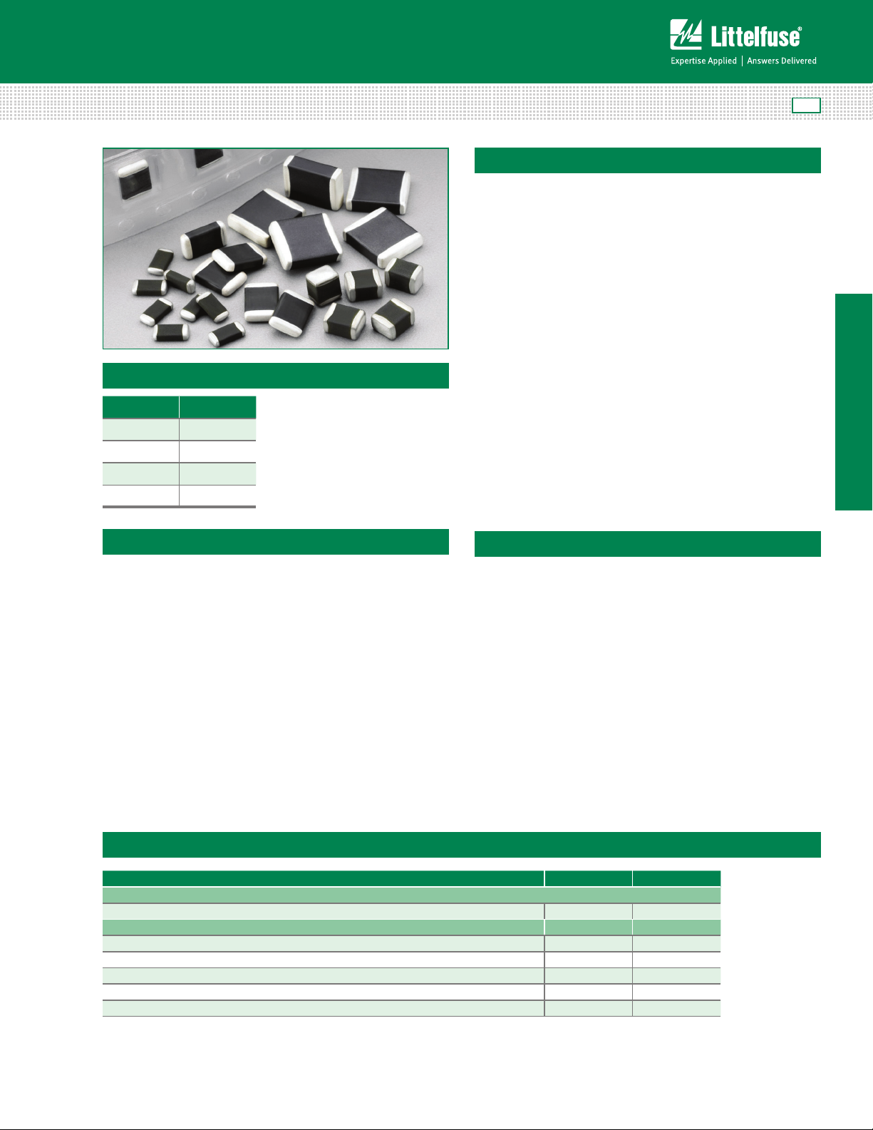
Surface Mount Multilayer Varistors (MLVs) > AUML Series
AUML Varistor Series
Size Table
Metric EIA
3216 1206
3225 1210
4532 1812
5650 2220
RoHS
Description
The AUML Series of Multilayer Transient Surge Suppressors
was specifically designed to suppress the destructive
transient voltages found in an automobile. The most common
transient condition results from large inductive energy
discharges. The electronic systems in the automobile, e.g.
antilock brake systems, direct ignition systems, engine
control, airbag control systems, wiper motor controls, etc.,
are susceptible to damage from these voltage transients and
thus require protection. The AUML transient suppressors
have temperature independent suppression characteristics
affording protection from -55ºC to 125ºC.
The AUML suppressor is manufactured from semiconducting
ceramics which offer rugged protection and excellent
transient energy absorption in a small package. The devices
are available in ceramic leadless chip form, eliminating lead
inductance and assuring fast speed of response to transient
surges. These Suppressors require significantly smaller
space and land pads than Silicon TVS diodes, offering greater
circuit board layout flexibility for the designer.
Also see the Littelfuse ML, MLN and MLE Series of
Multilayer Suppressors.
AUML Series
Applications
• Suppression of
inductive switching
or other transient
events such as EFT
and surge voltage at
the circuit board level
• ESD protection for
components sensitive
to IEC 61000-4-2, MILSTD-883C, Method
3015.7, and other
industry specifications
(See Also the MLE
or MLN Series)
• Provides on-board
transient voltage
protection for ICs
and transistors
• Used to help achieve
electromagnetic
compliance of
end products
• Replace larger surface
mount TVS Zeners in
many applications
Features
• AEC - Q200 compliant
• RoHS Compliant
• Load Dump energy
rated per SAE
Specification J1113
• Leadless, surface
mount chip form
• “Zero” Lead
Inductance
• Variety of energy
ratings available
• No temperature
derating up to
• High peak surge
current capability
• Low Profile, compact
industry standard
chip size; (1206, 1210,
1812 and 2220 Sizes)
• Inherent bidirectional
clamping
• No Plastic or epoxy
packaging assures
better than 94V-0
flammability rating
125ºC ambient
Absolute Maximum Ratings
• For ratings of individual members of a series, see Device Ratings and Specifications chart.
Continuous AUML Series Units
Steady State Applied Voltage:
DC Voltage Range (V
Transient:
Load Dump Energy, (WLD) 1.5 to 25 J
Jump Start Capability (5 minutes), (V
Operating Ambient Temperature Range (T
Storage Temperature Range (T
Temperature Coefficient (DV) of Clamping Voltage (V
CAUTION: Stresses above those listed in “Absolute Maximum Ratings” may cause permanent damage to the device. This is a stress only rating and operation of the device at these or any
other conditions above those indicated in the operational sections of this specification is not implied.
) -55 to +150
STG
) 18 V
M(DC)
) 24.5 V
) -55 to +125
A
JUMP
) at Specified Test Current
C
<0.01 %/OC
O
C
O
C
© 2013 Littelfuse, Inc.
Specifications are subject to change without notice.
Please refer to www.littelfuse.com/series/AUML.html for current information.
55
Revised: May 8, 2013
AUML Varistor Series
Page 2
Varistor Products
Surface Mount Multilayer Varistors (MLVs) > AUML Series
Device Ratings and Specifications
ºC
Maximum Ratings (125
Part Number
Maximum
Continuous
DC Voltage
V
M(DC)
Jump Start
Voltage
(5 Min)
V
JUMP
(V) (V) (J) (V) (V) (μA) (V) (A)
V18AUMLA1206 18 24.5 1.5 23 32 50 40 1.5
V18AUMLA1210 18 24.5 3.0 23 32 50 40 1.5
V18AUMLA1812 18 24.5 6.0 23 32 100 40 5.0
V18AUMLA2220 18 24.5 25 23 32 200 40 10.0
For automotive 24V and 42V applications please contact your Littelfuse representative or visit www.littelfuse.com for the latest product update.
NOTES: 1. Average power dissipation of transients not to exceed 0.1W, 0.15W, 0.3W and 1W for model sizes 1206, 1210, 1812 and 2220 respectively.
2. Load Dump energy rating (into the suppressor) of a voltage transient with a resultant time constant of 115ms to 230ms.
3. Thermal shock capability per Mil-Std-750, Method 1051: -55ºC to 125ºC, 5 minutes at 25ºC, 25 Cycles: 15 minutes at each extreme.
4. For application specific requirements, please contact Littelfuse.
) Specifications (25ºC)
Load Dump
Energy
(10 Pulses)
W
LD
Nominal Varistor Voltage
at 10mA
DC Test Current
V
Min V
N(DC)
Max I
N(DC)
Maximum
Standby Leakage
(at 13V DC)
Maximum Clamping
Voltage (V
Test Current (8/20μs)
L
V
C
C
) at
I
P
Current, Energy and Power Derating Curve
When transients occur in rapid succession, the average
power dissipation is the energy (watt-seconds) per pulse
times the number of pulses per second. The power so
developed must be within the specifications shown on the
Device Ratings and Characteristics Table for the specific
device. Certain parameter ratings must be derated at high
temperatures as shown below.
100
90
80
70
60
50
40
30
20
PERCENT OF RATED VALUE
10
0
-55 50 60 70 80 90 10 0 110 120 130 140 150
Figure 1
AMBIENT TEMPERATURE (oC)
Maximum Leakage Current/Clamping Voltage Curve for
AUML Series at 25ºC
Peak Pulse Current Test Waveform for Clamping Voltage
100
50
0
PERCENT OF PEAK VALUE
O
1
Figure 2
T
T
1
T
2
TIME
01 = Virtual Origin of Wave
T = Time from 10% to 90% of Peak
T1 = Rise Time = 1.25 x T
T2 = Decay Time
Example - For an 8/20 μs Current Waveform:
8μs = T
= Rise Time
1
20μs = T
= Decay Time
2
Typical V-I Characteristics of the V18AUMLA2220 at -40ºC,
25ºC, 85ºC and 125ºC
100
10
VOLTA GE
1
Figure 3 Figure 4
AUML Varistor Series
MAXIMUM LEAKAGE MAXIMUM CLAMPING VOLTAGE
1210/1206
1812
2220
10mA
CURRENT
100mA
1mA
100μA10μA
1A 10A
1210/1206
1812
2220
100A
Revised: May 8, 2013
100
10
VOLTA GE
1
56
-40oC
25oC
85oC
125oC
1μA 10μA 100μA
Please refer to www.littelfuse.com/series/AUML.html for current information.
10mA 100mA 1A 10A 100A 1000A
1mA
CURRENT
Specifications are subject to change without notice.
© 2013 Littelfuse, Inc.
Page 3
Varistor Products
Surface Mount Multilayer Varistors (MLVs) > AUML Series
Temperature Effects
In the leakage region of the AUML suppressor, the device
characteristics approaches a linear (ohmic) relationship
and shows a temperature dependent affect. In this region
the suppressor is in a high resistance mode (approaching
106Ω) and appears as a near open-circuit. Leakage currents
at maximum rated voltage are in the microamp range.
Load Dump Energy Capability
A Load Dump transient occurs when the alternator load in
the automobile is abruptly reduced. The worst case scenario
of this transient occurs when the battery is disconnected
while operating at full rated load. There are a number of
different Load Dump specifications in existence in the
automotive industry, with the most common one being that
recommended by the Society of Automotive Engineers,
specification #SAE J1113. Because of the diversity of these
Load Dump specifications Littelfuse defines the Load
Dump energy capability of the AUML suppressor range as
that energy dissipated by the device itself, independent
of the test circuit setup. The resultant Load Dump energy
handling capability serves as an excellent figure of merit for
the AUML suppressor. Standard Load Dump specifications
require a device capability of 10 pulses at rated energy,
across a temperature range of -40ºC to +125ºC. This
capability requirement is well within the ratings of all of the
AUML Series (Figure 6 on next page).
Further testing on the AUML Series has concentrated
on extending the number of Load Dump pulses, at rated
energy, which are applied to the devices. The reliability
information thus generated gives an indication of the
inherent capability of these devices. As an example of
device durability the 1210 size has been subjected to over
2000 pulses at its rated energy of 3 joules (J); the 1812 size
has been pulsed over 1000 times at 6J and 2220 size has
been pulsed at its rated energy of 25J over 300 times. In
all cases there has been little or no change in the device
characteristics (Figure 7 on next page).
When clamping transients at higher currents (at and above
the 10mA range), the AUML suppressor approaches
a 1-10 characteristic. In this region the characteristics
of the AUML are virtually temperature independent.
Figure 3 shows the typical effect of temperature on
the V-I characteristics of the AUML suppressor.
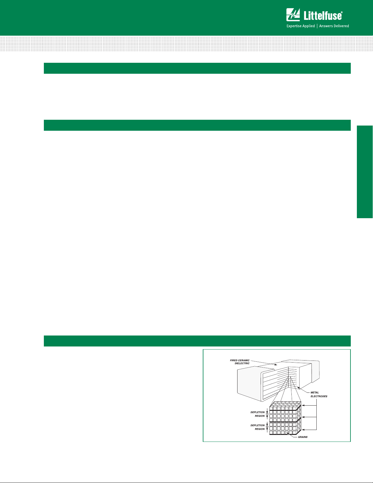
The very high energy absorption capability of the AUML
suppressor is achieved by means of a highly controlled
manufacturing process. This technology ensures that a
large volume of suppressor material, with an interdigitated
layer construction, is available for energy absorption in an
extremely small package. Unlike equivalent rated Silicon
TVS diodes, the entire AUML device volume is available to
dissipate the Load Dump energy.
Hence, the peak temperatures generated by the Load
Dump transient are significantly lower and evenly dissipated
throughout the complete device (Figure 5 below). This
even energy dissipation ensures that there are lower peak
temperatures generated at the P-N grain boundaries of the
AUML suppressor.
There are a number of different size devices available in the
AUML Series, each one with a load dump energy rating,
which is size dependent.
Experience has shown that while the effects of a load dump
tranient is of real concern, its frequency of occurrence is
much less than thoe of low energy inductive spikes. Such
low energy inductive spikes may be generated as a result
of motors switching on and off, from ESD occurrances, fuse
blowing, etc. It is essential that the suppression technology
selected also has the capability to suppress such transients.
Testing on the V18AUMLA2220 has shown that after being
subjected to a repetitive energy pulse of 2J, over 6000
times, no characteristic changes have occurred (Figure 8 on
next page).
AUML Series
Speed of Response
The clamping action of the AUML suppressor depends
on a conduction mechanism similar to that of other
semiconductor devices (i.e. P-N Junctions). The apparent
slow response time often associated with transient
voltage suppressors (Zeners, MOVs) is often due to
parasitic inductance in the package and leads of the
device and less dependent of the basic material (Silicon,
Z
O). Thus, the single most critical element affecting the
N
response time of any suppressor is its lead induc-tance.
The AUML suppressor is a surface mount device, with no
leads or external packaging, and thus, it has virtually zero
inductance. The actual response time of a AUML surge
suppressor is in the 1 to 5 ns range, more than sufficient
for the transients which are likely to be encountered in an
automotive environment.
© 2013 Littelfuse, Inc.
Specifications are subject to change without notice.
Please refer to www.littelfuse.com/series/AUML.html for current information.
57
Revised: May 8, 2013
Multilayer Internal Construction
Figure 5
AUML Varistor Series
Page 4

Varistor Products
0
Surface Mount Multilayer Varistors (MLVs) > AUML Series
AUML Load Dump Pulsing over a Temperature Range of
-55ºC to +125ºC
V(10mA)
35
30
25
20
15
VOLTA GE
10
5
0
012345678 9101
Figure 6
# OF LOAD DUMPS
2220 = 25J
1812 = 6J
1210 = 3J
112
Repetitive Load Dump Pulsing at Rated Energy
V(10mA)
35
30
25
20
15
VOLTA GE
10
5
0
0 50 100 150 200 250 300 350 1,0 00 2,
Figure 7
# OF LOAD DUMPS
2220 = 25J
1812 = 6J
1210 = 3J
00
Explanation of Terms
Maximum Continuous DC Working Voltage (*V
M*(DC)+
)
+
This is the maximum continuous DC voltage which may
be applied, up to the maximum operating temperature
(125ºC), to the ML suppressor. This voltage is used as the
reference test point for leakage current and is always less
than the breakdown voltage of the device.
Load Dump Energy Rating *W
+
LD
This is the actual energy the part is rated to dissipate
under Load Dump conditions (not to be confused with the
"source energy" of a Load Dump test specification).
Maximum Clamping Voltage *V
+
C
This is the peak voltage appearing across the suppressor
when measured at conditions of specified pulse current
and specified waveform (8/20μs). It is important to note
that the peak current and peak voltage may not necessarily
be coincidental in time.
Leakage Current *I
+
L
In the nonconducting mode, the device is at a very
high impedance (approaching 10
6
Ω at its rated working
voltage) and appears as an almost open circuit in the
system. The leakage current drawn at this level is very
low (<25μA at ambient temperature) and, unlike the
Zener diode, the multilayer TVS has the added advantage
that, when operated up to its maximum temperature,
its leakage current will not increase above 500μA.
Repetitive Energy Testing of V18AUMLA2220
at an Energy Level of 2 Joules
V AT 10mA
100
VOLTA GE
10
1000 2000 3000 4000 5000 6000 7000
Figure 8
AUML Varistor Series
NUMBER OF PULSES
V18AUMLA2220
Nominal Voltage *V
N*DC+
+
This is the voltage at which the AUML enters its
conduction state and begins to suppress transients.
In the automotive environment this voltage is
defined at the 10mA point and has a minimum
(V
58
Revised: May 8, 2013
) and maximum (V
N(DC) MIN
) voltage specified.
N(DC) MAX
Please refer to www.littelfuse.com/series/AUML.html for current information.
Specifications are subject to change without notice.
© 2013 Littelfuse, Inc.
Page 5

Varistor Products
Surface Mount Multilayer Varistors (MLVs) > AUML Series
Lead (Pb) Soldering Recommendations
The principal techniques used for the soldering of
components in surface mount technology are IR Re-flow
and Wave soldering. Typical profiles are shown on the right.
The termination option available for each solder technique is:
Reflow Wave
1. Nickel Barrier (preferred) 1. Nickel Barrier (preferred)
2. Silver/Platinum
The recommended solder for the AUML suppressor is
a 62/36/2 (Sn/Pb/Ag), 60/40 (Sn/Pb) or 63/37 (Sn/Pb).
Littelfuse also recommends an RMA solder flux.
Wave soldering is the most strenuous of the processes.
To avoid the possibility of generating stresses due to
thermal shock, a preheat stage in the soldering process
is recommended, and the peak temperature of the solder
process should be rigidly controlled.
When using a reflow process, care should be taken to
ensure that the AUML chip is not subjected to a thermal
gradient steeper than 4 degrees per second; the ideal
gradient being 2 degrees per second. During the soldering
process, preheating to within 100 degrees of the solder's
peak temperature is essential to minimize thermal shock.
Once the soldering process has been completed, it
is still necessary to ensure that any further thermal
shocks are avoided. One possible cause of thermal
shock is hot printed circuit boards being removed from
the solder process and subjected to cleaning solvents
at room temperature. The boards must be allowed to
cool gradually to less than 50ºC before cleaning.
Reflow Solder Profile
Figure 9
Wave Solder Profile
300
250
C)
200
o
150
100
TEMPERATURE (
50
0
Figure 10
0.0 0.5 1.0 1.5 2.0 2.5 3.0 3.5 4.0 4.5
230
AUML Series
MAXIMUM WAVE 260oC
SECOND PREHEAT
FIRST PREHEAT
TIME (MINUTES)
Lead–free (Pb-free) Soldering Recommendations
Littelfuse offers the Nickel Barrier Termination finish for the
optimum Lead–free solder performance.
The preferred solder is 96.5/3.0/0.5 (SnAgCu) with an RMA
flux, but there is a wide selection of pastes and fluxes
available with which the Nickel Barrier parts should be
compatible.
The reflow profile must be constrained by the maximums
in the Lead–free Reflow Profile. For Lead–free Wave
soldering, the Wave Solder Profile still applies.
Note: the Lead–free paste, flux and profile were used for
evaluation purposes by Littelfuse, based upon industry
standards and practices. There are multiple choices of all
three available, it is advised that the customer explores the
optimum combination for their process as processes vary
considerably from site to site.
© 2013 Littelfuse, Inc.
Specifications are subject to change without notice.
Please refer to www.littelfuse.com/series/AUML.html for current information.
Lead–free Re-flow Solder Profile
59
Revised: May 8, 2013
Figure 11
MAXIMUM TEMPERATURE 260˚C
20 - 40 SECONDS WITHIN 5˚C
RAMP RATE
<3˚C/s
PREHEAT ZONE
60 - 150 SEC
> 217˚C
5.0 6.0 7.0
AUML Varistor Series
Page 6

Product Dimensions (mm)
PAD LAYOUT DIMENSIONS CHIP LAYOUT DIMENSIONS
Varistor Products
Surface Mount Multilayer Varistors (MLVs) > AUML Series
E
L
SYMBOL
Note: Avoid metal runs in this area, parts are not recommended
for use in applications using Silver (Ag) epoxy paste.
1206 Size 1210 Size 1812 Size 2220 Size
IN MM IN MM IN MM IN MM
D
W
A 0.203 5.150 0.219 5.510 0.272 6.910 0.315 8.000
B 0.103 2.620 0.147 3.730 0.172 4.360 0.240 6.190
C 0.065 1.650 0.073 1.850 0.073 1.850 0.073 1.850
D (max.) 0.071 1.80 0.070 1.80 0.07 1.80 0.118 3.00
E 0.020 -/+ 0.010 0.50 -/+0.25 0.020 -/+ 0.010 0.50 -/+ 0.25 0.020 -/+ 0.010
L 0.125 -/+ 0.012 3.20 -/+ 0.03 0.125 -/+ 0.012 3.20 -/+ 0.30 0.180 -/+ 0.014
W 0.060 -/+ 0.011 1.60 -/+ 0.28 0.100 -/+ 0.012 2.54 -/+ 0.30 0.125 -/+ 0.012
0.50 -/+
0.25
4.50 -/+
0.35
3.20 -/+
0.30
0.030 -/+ 0.010 0.75 -/+ 0.25
0.225 -/+ 0.016 5.70 -/+ 0.40
0.197 -/+ 0.016 5.00 -/+ 0.40
Part Numbering System
V
18 AUML
DEVICE FAMILY
TVSS Device
MAXIMUM DC
WORKING VOLTAGE
AUTOMOTIVE
MULTILAYER DESIGNATOR
LOAD DUMP ENERGY RATING
INDICATOR
A 2220 X X
PACKING OPTIONS
A: Bulk Pack, 2500 pieces
H: 7in (178mm) Diameter Reel*
T: 13in (330mm) Diameter Reel*
* See quanttities in Packaging table below
END TERMINATION OPTION
No Letter: Ag/P
N: Nickel Barrier
DEVICE SIZE
i.e., 220 mil x 200 mil
2220 size only
t
Packaging*
Quantity
Device Size
1206 10,000 2,500 2,500
1210 8,000 2,000 2,000
1812 4,000 1,000 1,000
2220 4,000 1,000 1,000
*(Packaging) It is recommended that parts be kept in the sealed bag provided and that parts be used as soon as possible when removed from bags.
AUML Varistor Series
13” Inch Reel
('T' Option)
7” Inch Reel
('H' Option)
Bulk Pack
('A' Option)
Revised: May 8, 2013
60
Please refer to www.littelfuse.com/series/AUML.html for current information.
Specifications are subject to change without notice.
© 2013 Littelfuse, Inc.
Page 7

Varistor Products
Surface Mount Multilayer Varistors (MLVs) > AUML Series
Tape and Reel Specifications
Symbol Description Dimensions in Millimeters
A
B
K
W Width of Tape 8 -/+ 0.2 12 -/+ 0.2
P
P
P
D
D
T
T
NOTE: Dimensions in millimeters.
• Conforms to EIA-481-1, Revision A
• Can be supplied to IEC publication 286-3
Tape 8mm Wide Tape 12mm Wide Tape
Chip Size 1206 1210 1812 2220
Width of Cavity Dependent on Chip Size to Minimize Rotation.
0
Length of Cavity Dependent on Chip Size to Minimize Rotation.
0
Depth of Cavity Dependent on Chip Size to Minimize Rotation.
0
F Distance Between Drive Hole Centers and Cavity Centers 3.5 -/+ 0.5 5.4 -/+ 0.5
E Distance Between Drive Hole Centers and Tape Edge 1.75 -/+ 0.1 1.75 -/+ 0.1
Distance Between Cavity Center 4 -/+ 0.1 8-/+ 0.1
1
Axial Distance Between Drive Hole Centers and Cavity Centers 2 -/+ 0.1 2 -/+ 0.1
2
Axial Distance Between Drive Hole Centers 8 -/+ 0.1 8 -/+ 0.1
0
Drive Hole Diameter 1.55 -/+ 0.05 1.55 -/+ 0.05
0
Diameter of Cavity Piercing 1.05 -/+ 0.05 1.55 -/+ 0.05
1
Embossed Tape Thickness 0.3 Max 0.4 Max
1
Top Tape Thickness 0.1 Max 0.1 Max
2
AUML Series
Standard Packaging
Tape and reel is the standard packaging method of the
AUML Series. The standard 300 millimeter (13–inch) reel
utilized contains 4000 pieces for the 2200 and 1812 chips,
8000 pieces for the 1210 chip and 10,000 pieces for the
1206 size.
To order: add 'T' to the standard part number,
e.g.V18AUMLA222OT.
© 2013 Littelfuse, Inc.
Specifications are subject to change without notice.
Please refer to www.littelfuse.com/series/AUML.html for current information.
Special Packaging
Option1: 178 millimeter (7–inch) reels containing 1000
Option 2 For small sample quantities (less than 100
e.g. V18AUMLA2220A.
61
Revised: May 8, 2013
(2220, 1812), 2000 (1210), 2500 (1206), pieces
are available. To order add 'H' to the standard
part number, e.g. V18AUMLA2220H.
pieces) the units are shipped bulk pack. To
order add 'A' to the standard part number,
AUML Varistor Series
 Loading...