

Page 1
RoHS
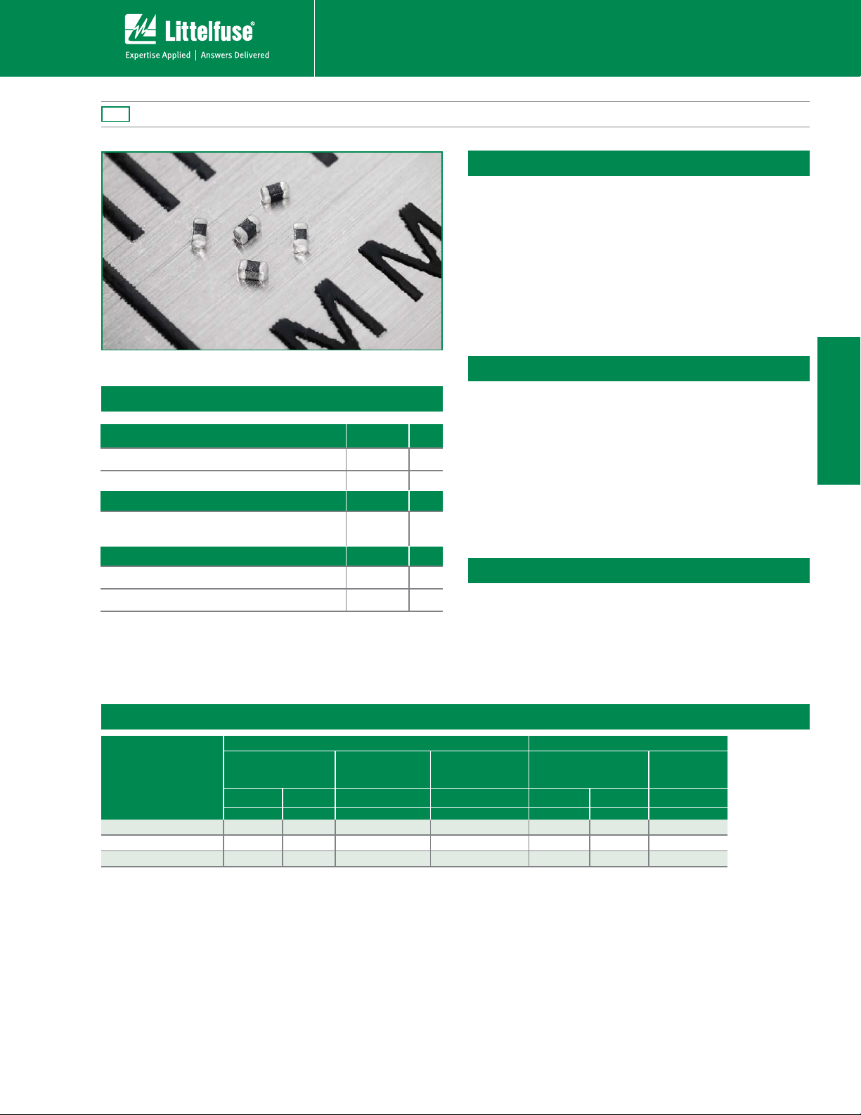
0201 MLA Varistor Series
Varistor Products
Surface Mount Multilayer Varistors (MLVs) > 0201 MLA Series
Description
New 0201-size MLA Multi-Layer Varistor (MLV) series can
protect small electronic products from electrostatic discharge
(ESD) and electrically fast transients (EFT).
It's ultra-compact 0201 size, the smallest form factor available
for MLV devices, is ideal for compact handheld products.
The ML Series is manufactured from semiconducting ceramics,
and is supplied in a leadless, surface mount package.
Plating consists of Silver base material (which is fired on to the
Zno dialectric), Nickel barrier plated under-layer and Matte-Tin
outer surface plate.
Features
Absolute Maximum Ratings
Steady State Applied Voltage:
Maximum DC Voltage (V
Maximum AC Voltage (V
Transient:
Non-Repetitive Surge Current, 8/20μs
Waveform, (I
)
TM
) 5.5 V
M(DC)
) 4.0 V
M(AC)RMS
Unit
4.0 A
• Ultra-small 0201 size for
minimal board space
• Low capacitance (33pF)
for high data rates to
minimize signal distortion
• Meets IEC 610004-2 for ESD
• Low leakage (<25μa)
• Multilayer ceramic
construction technology
• Inherently Bi-directional
• Stable performance
over wide operating and
storage temperature
range -40°C to +85°C
• Operating voltage
V
M(DC)
• Rated for surge
current (8 x 20μs)
Temperature:
Operating Ambient Temperature Range (T
Storage Temperature Range (T
) -40 to +85 ºC
STG
) -40 to +85 ºC
A
Applications
• Portable / handheld
electronic devices
• Mobile communications
/ cellular phones
• USB, video and audio ports
• Data, diagnostic I/O ports
• Computer / DSP products
• Industrial instruments
including non-life sustaing
medical equipment
• Analog signal / sensor lines
Device Ratings and Specifications
Maximum Ratings @ +85ºC
Part Number
Maximum Continuous
Working Voltage
V
M(DC)
(V) (V) (A) (V) (V) (V) (pF)
V
M(AC)
Maximum Nonrepetitive Surge
Current (8/20μs)
I
TM
Maximum
Clamping Voltage
at 1A (8/20μs)
V
C
V5.5MLA020133NR 5.5 4.0 1 28.0* 8.0 14.0 33.0
V5.5MLA020147NR 5.5 4.0 1 26.0* 8.0 14.0 47.0
V5.5MLA020164NR 5.5 4.0 1 26.0* 8.0 14.0 64.0
Notes:
- Typical leakage at 25ºC at V
- End surface finish of Matte-Tin with Nickel under-layer on Silver base material
- Standard packing quantity 15,000 per reel, 7" reel
: 0201 size <10μA typical, <25μA maximum
M(DC)
Specifications @ +25ºC
Nominal Voltage at 1mA
DC Test Current
V
N(DC)
Min V
Max C
N(DC)
Typical
Capacitance at
f = 1MHz
0201 MLA Series
= 5.5V
©2010 Littelfuse, Inc.
Specifications are subject to change without notice.
Please refer to www.littelfuse.com/series/0201MLA.html for current information.
Revision: June 28, 2010
0201 MLA Varistor Series
Page 2
Varistor Products
Surface Mount Multilayer Varistors (MLVs) > 0201 MLA Series
Reliability and Environmental Specifications
Judge Criteria Test Condition
Solderability > 95% solder coverage 245 +/- ºC, 3 +/- 1 sec.
Leaching Resistance > 95% solder coverage 245 +/- ºC, 3 +/- 1 sec.
High Temperature Exposure
Thermal Shock
Operating Life
Bias Humidity
Δ Vv / Vv < 10% 1000 hours 85ºC, un-powered
Δ Vv / Vv < 10% -45 to +85 ºC, 30 min. cycle, 5 cycles
Δ Vv / Vv < 10% 85 ºC, DC working voltage 1000 hours
Δ Vv / Vv < 10% 40 ºC / 85% RH, DC working voltage 1000 hours
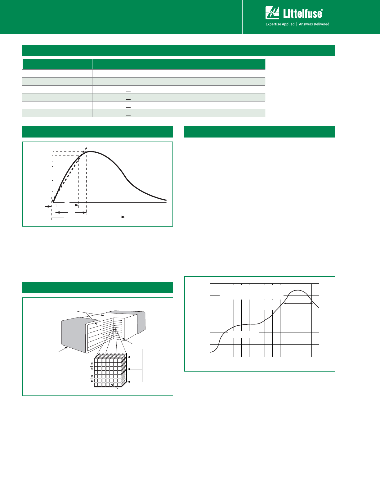
Peak Pulse Current Test Waveform for Clamping Voltage
100
50
0
PERCENT OF PEAK VALUE
O
1
T
T
1
T
2
01 = Virtual Origin of Wave
T = Time from 10% to 90% of Peak
T1 = Rise Time = 1.25 x T
T2 = Decay Time
Example - For an 8/20 μs Current Waveform:
8μs = T1 = Rise Time
20μs = T2 = Decay Time
Multilayer Internal Construction
FIRED CERAMIC
DIELECTRIC
TIME
Lead–free (Pb-free) Soldering Recommendations
To avoid the possibility of generating stresses due to
thermal shock, a preheat stage in the soldering process
is recommended, and the peak temperature of the solder
process should be rigidly controlled.
When using a reflow process, care should be taken to
ensure that the ML chip is not subjected to a thermal
gradient steeper than 4 degrees per second; the ideal
gradient being 2 degrees per second. During the soldering
process, preheating to within 100 degrees of the solder's
peak temperature is essential to minimize thermal shock.
Once the soldering process has been completed, it is
still necessary to ensure that any further thermal shocks
are avoided. One possible cause of thermal shock is hot
printed circuit boards being removed from the solder
process and subjected to cleaning solvents at room
temperature. The boards must be allowed to cool gradually
to less than 50º C before cleaning.
300
250
200
150
MAXIMUM TEMPERATURE 260˚C,
TIME WITHIN 5˚C OF PEAK
20 SECONDS MAXIMUM
RAMP RATE
<3˚C/s
60 - 150 SEC
> 217˚C
METAL END
TERMINATION
0201 MLA Varistor Series
DEPLETION
REGION
DEPLETION
REGION
GRAINS
METAL
ELECTRODES
Revision: June 28, 2010
100
TEMPERATURE °C
50
0
0 1.0 2.0 3.0 4.0 5.0 6.0 7.0
PREHEAT ZONE
TIME (MINUTES)
Please refer to www.littelfuse.com/series/0201MLA.html for current information.
Specifications are subject to change without notice.
©2010 Littelfuse, Inc.
Page 3

Product Dimensions (mm)
Varistor Products
Surface Mount Multilayer Varistors (MLVs) > 0201 MLA Series
PAD LAYOUT DIMENSIONS
C
B
NOTE : Avoid metal runs in this area, parts not
recommended for use in applications using
Silver (Ag) epoxy paste.
NOTE
A
Part Numbering System
V 5.5 0201
MLA xx N
DEVICE FAMILY
Littelfuse TVSS Device
MAXIMUM DC
WORKING VOLTAGE
MULTILAYER SERIES
DESIGNATOR
DEVICE SIZE:
0201 = .024 inch x .012 inch
(0.6 mm x 0.3 mm)
CHIP LAYOUT DIMENSIONS
E
D
W
L
R
PACKING OPTIONS
R = 7in (178mm) Diameter Reel, Paper Carrier Tape
15,000 items per reel
END TERMINATION OPTION
N = Nickel Barrier Option
(Matte Tin outer surface, plated on Nickel underlayer
plated on silver base metal)
CAPACITANCE OPTION
33 = 33pF
47 = 47pF
64 = 64pF
Dimension
0201 Size
IN MM
A 0.055 1.40
B 0.020 0.50
C 0.020 0.50
D (max.) 0.014 0.35
E 0.008 -/+0.004 0.20 -/+0.10
L 0.024 -/+0.002 0.60 -/+0.05
W 0.012 -/+0.002 0.30 -/+0.05
0201 MLA Series
Tape and Reel Specifications
D
0
K
0
t
D
1
1
Symbol Description
A
Width of Cavity 0.36 -/+0.02
0
Length of Cavity 0.70 -/+0.02
B
0
W Width of Tape 8.0 -/+0.1
F Distance Between Drive Hole Centers and Cavity Centers 3.5 -/+0.05
E Distance Between Drive Hole Centers and Tape Edge 1.75 -/+0.05
Distance Between Cavity Centers 2.0 -/+0.05
P
1
Axial Drive Distance Between Drive Hole Centers & Cavity Centers 2.0 -/+0.05
P
2
Axial Drive Distance Between Drive Hole Centers 4.0 -/+0.1
P
0
Drive Hole Diameter 1.55 -/+0.05
D
0
Top Tape Thickness 0.42 -/+0.02
T
1
NOTE: It is recommended that parts be kept in the sealed bag provided and that parts be used as soon as possible when removed from bags.
P
0
P
2
E
F
B
0
P
1
A
0
For T and H Pack Options: PLASTIC CARRIER TAPE
For R Pack Options: EMBOSSED PAPER CARRIER TAPE
W
EMBOSSMENT
TOP TAPE
Dimensions in
Millimeters
0201
8mm
NOMINAL
PRODUCT
IDENTIFYING
LABEL
178mm
OR 330mm
DIA. REEL
©2010 Littelfuse, Inc.
Specifications are subject to change without notice.
Please refer to www.littelfuse.com/series/0201MLA.html for current information.
Revision: June 28, 2010
0201 MLA Varistor Series
 Loading...