

Page 1
Data Sheet: CR Series
JukeBlox Networked Media Modules
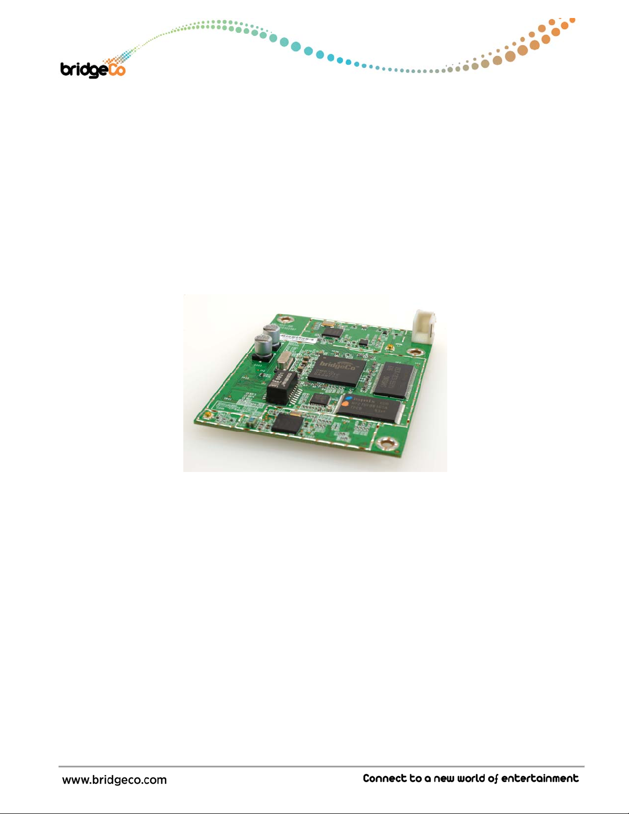
JukeBlox Networked Media Module
CR Series
Datasheet
Complete audio networking system on a small module
Integrated Ethernet + USB2.0
WiFi-certified 802.11b/g (optional)
Built-in PIFA antenna
DAB radio receiver (optional)
Glueless audio, video and control ports
FCC certified
CONFIDENTIAL
dat_CR860_CR870_2_5_datasheet.doc CONFIDENTIAL Version 2.5 – February 10th 2010 - Page 1 of 13
Page 2
Data Sheet: CR Series
JukeBlox Networked Media Modules
Introduction
The CR-series module is a single-board networked media player module, based on BridgeCo’s DM860
and DM870 media processors, and enables fast product developments with Ethernet, USB and
optional WiFi and/or DAB radio connectivity. The module connects to standard legacy components in
various audio, video/LCD and control formats.
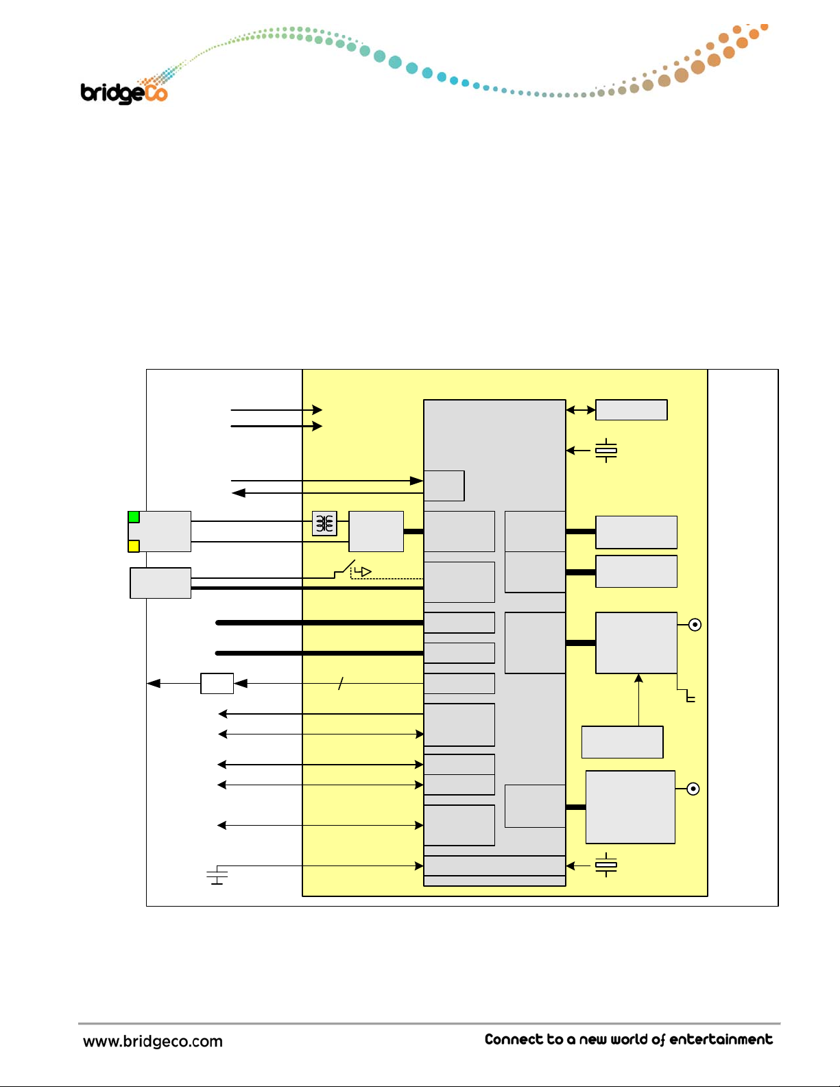
Block Diagram
JukeBlox Networked Media Module – CR Series
3.3V
1.2V
Reset In
Reset Out
DM860
or
DM870
RST
JTAG
24.000 MHz
100B-T
USB
HP out
RJ-45
USB
(Host)
SD-Card
CCIR-656
A/D, D/A
serial control
shift register
IC control
IR sensor
reset signals
analog mute
SuperCap
Display
S/PDIF
2
I
C bus
LP
max. 20 GPIOs
3x6bit RGB
4/8bit MMC
Stereo Out
Video Out
Audio I/O
2 x UART
SPI Ctrl.
3.3V (RTC)
Ethernet
2
PHY
5V
RMII
USB
LCD
SSM
DAC
AV
Ports
UART
SPI
GPIO
RTC
NAND
Mem
802.11
AV
Ports
1 GB
NAND flash
256 Mbit
SDRAM
802.11
RF amp
(optional)
Switcher
1.9V
DAB
32.768 kHz
PIFA
Antenna
dat_CR860_CR870_2_5_datasheet.doc CONFIDENTIAL Version 2.5 – February 10th 2010 - Page 2 of 13
Page 3
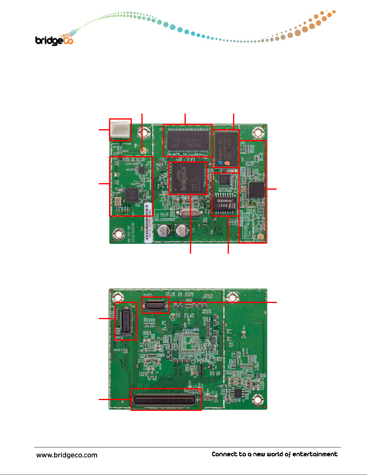
Overview
p
Data Sheet: CR Series
JukeBlox Networked Media Modules
Top View
PIFA
antenna
802.11b/g
front-end
Bottom View
DAB
connector
Media
connector
antenna
connector
SDRAM
BridgeCo
rocessor
FLASH
(optional socket)
LCD
connector
dat_CR860_CR870_2_5_datasheet.doc CONFIDENTIAL Version 2.5 – February 10th 2010 - Page 3 of 13
Page 4
Data Sheet: CR Series
JukeBlox Networked Media Modules
Ordering Guide
Part
Number
CR870-2A DM870+T6201 X X X X X X X
CR870-2B DM870+T6201 X X X X X
CR870-2C DM870+T6201 X X X X
CR870-2D DM870+T6201 X X X X X
CR870-2F DM870+T6201 X X X X X X
CR860-2A DM860 n/a X X n/a
CR860-2B DM860 n/a X X X X n/a
BridgeCo ICs
WiFi Ethernet USB
Contains
shield
Incl. connector
Real-Time
Clock
DAB / DAB+ /
DMB Audio
LCD
Incl.
connector
PIFA
Ant.
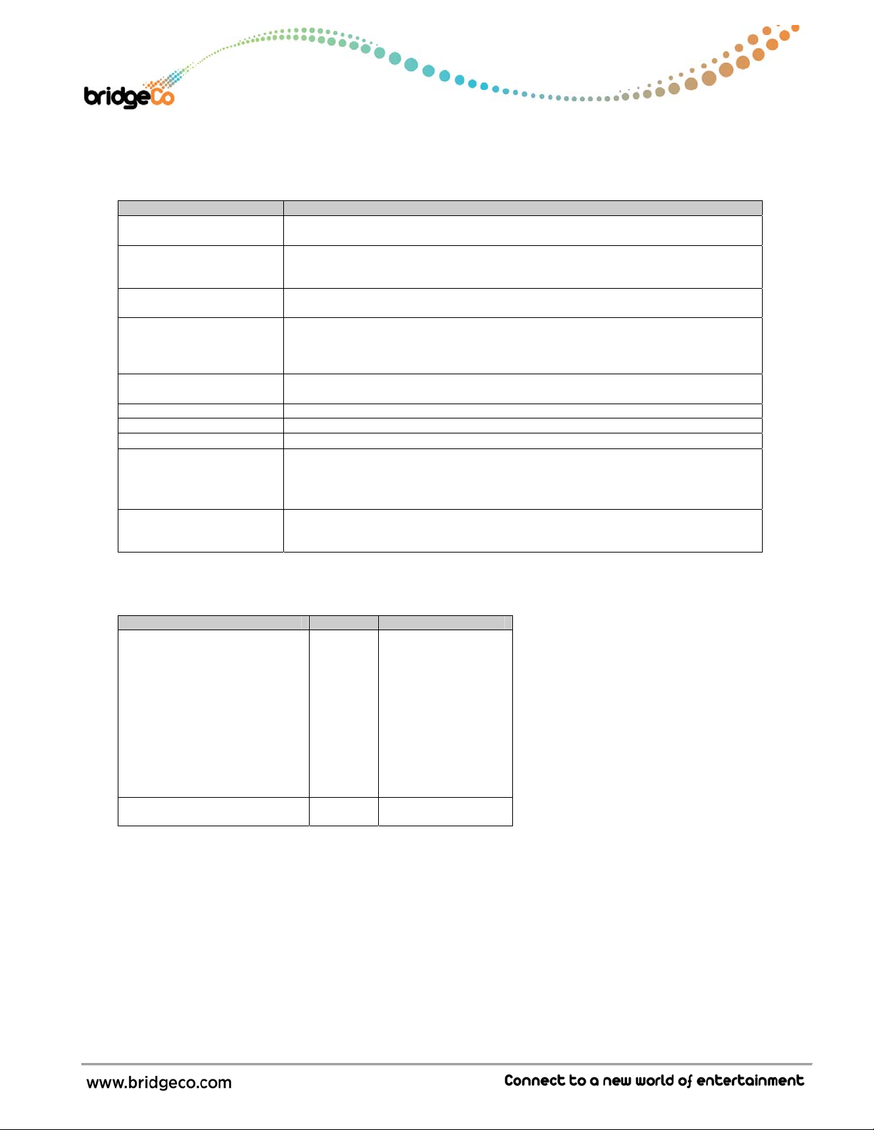
Electrical Specifications
Parameter State Model Component Symbol min. typ. max. Units
Input Voltage
Power
Consumption
Reset State CR870
WLAN
Operating
Main VIN
DAB VIN
CR860
CR870
CR860
PIN
PIN
+2.97
+1.08
+1.62
+2.97
+1.35
tbd
tbd
tbd
tbd
+3.3
+1.2
+1.8
+3.3
+1.5
tbd
tbd
tbd
tbd
+3.63
+1.32 V V
+1.98
+3.63
+1.65
tbd
tbd
tbd
tbd
V
V
V
W
W
W
W
Operating Conditions
Parameter min. max. Units
Operating Temperature 0 +70 °C
Operating Humidity 10 90 (non condensing) %RH
Storage Temperature -10 +75 °C
Storage Humidity 10 95 (non condensing) %RH
Storage Temperature Cycle Test 24 hrs -10 +75 °C
dat_CR860_CR870_2_5_datasheet.doc CONFIDENTIAL Version 2.5 – February 10th 2010 - Page 4 of 13
Page 5
WiFi Specification (CR870 only)
Feature Description
WLAN Standards IEEE 802.11b
Frequency Band 2.412 – 2.497 GHz (2.4GHz ISM Band, 14 Channels)
Modulation 802.11b mode (DS-SS: IEEE 802.11b)
Transmission Speed 802.11b mode
Tx Power 802.11b mode (16.5dBm, +/-1dBm)
Power-on Ramp < 2us
RF Carrier Suppression < 15dBc
TX EVM < -5dB
Rx Sensitivity
(incl. CE2 Mother board)
Throughput Rate
(measured for each
module)
IEEE 802.11g
Channel 1 - Channel 13, Channel 14
North America, Japan Telec, Europe ETSI
802.11g mode (OFDM: IEEE 802.11g)
11Mbps, 5.5Mbps, 1Mbps
802.11g mode
54Mbps, 48Mbps, 36Mbps, 24Mbps, 18Mbps, 12Mbps, 9Mbps, 6Mbps
802.11g mode (21dBm, +/-1dBm)
802.11b mode
=<-88dBm @ 1Mbps, =<-85dBm @ 5.5Mbps, =<-83dBm @ 11Mbps
802.11g mode
=<-86dBm @ 6Mbps, =<-75dBm @ 36Mbps, =<-69dBm @ 54Mbps
See factory test specification
Data Sheet: CR Series
JukeBlox Networked Media Modules
Regulatory compliance
Description Country Compliance
Electromagnetic Compatibility
(Prescan)
Radio Regulations (CM870
only)
USA
Europe
TBD TBD
FCC CFR47 Part15B
EN 55022
EN 55024
EN 61000-3-2
EN 61000-3-3
EN 61000-4-2
EN 61000-4-3
EN 61000-4-4
EN 61000-4-5
EN 61000-4-6
EN 61000-4-8
EN 61000-4-11
dat_CR860_CR870_2_5_datasheet.doc CONFIDENTIAL Version 2.5 – February 10th 2010 - Page 5 of 13
Page 6

Data Sheet: CR Series
JukeBlox Networked Media Modules
RoHS
Uses only RoHS compliant components
Environmental Test
Withstands 4 hours at 70°C, 90% RH
ESD and Transient Test (Applies to LAN and USB external
connections only)
ESD: +/- 2kV operation, +/- 4kV no destruction (part of CE test)
Fast electrical transients: +/- 500V operation, +/- 1000V no destruction (part of CE test)
Magnetic Field Test
Passes EN55022 and EN55024 (part of CE test)
MTBF
>10000 hours
Mechanical Specifications
Passes drop test according to I.E.C. 68-2-32, height 100 cm, 1 corner, 6 faces.
Passes vibration test with sine, vertical, 60 minutes, 600 to 18000 cpm, 1G
Module Quality
Defect Rate: 7 months <0.5% failures, 14 months <1% failures
AQL CR=0, MA=0.4, MI=0.4
dat_CR860_CR870_2_5_datasheet.doc CONFIDENTIAL Version 2.5 – February 10th 2010 - Page 6 of 13
Page 7

Board Dimensions
Top View and Side View
Data Sheet: CR Series
JukeBlox Networked Media Modules
Bottom View (showing connector locations)
Note:
1. All dimensions are measured in millimetres (mm).
2. PCB’s thickness: 1.00 +/- 0.10mm
3. Tolerance: +/-0.10mm
4. Outline Tolerance: +/-0.10mm
5. NPTH Hole: +/-0.05mm
6. PTH Hole: +/-0.075mm
dat_CR860_CR870_2_5_datasheet.doc CONFIDENTIAL Version 2.5 – February 10th 2010 - Page 7 of 13
Page 8

Data Sheet: CR Series
JukeBlox Networked Media Modules
Module weight
CR860-1: 25g
CR870-1: 25g
Connectors
WLAN Antenna Connectors (optional)
One coaxial antenna connector is provided as an alternative to the built-in PIFA antenna. The choice
between using the PIFA antenna or using the coaxial socket is a bu ild option, determined by the
position of a surface mount capacitor on the module PCB. Please see ordering guide for build option
details.
The surface-mount receptible parts:
Hirose
U.FL-R-SMT (CL No. 331-0471-0)
Coaxial antenna connector dimensions
Module Connectors
The CR860/CR870 module uses 3 male connectors as interfaces to the main board, described below.
Connector
Number
J1 LCD 30 2 x 15 x 0.5mm 24-5046-030-100-829 (Kyocera)
J2 Media 120 2 x 60 x 0.5mm 24-5046-120-100-829 (Kyocera)
J3 DAB
dat_CR860_CR870_2_5_datasheet.doc CONFIDENTIAL Version 2.5 – February 10th 2010 - Page 8 of 13
Connector
Purpose
Connector
Type
B2B
Connector
Number
of Pins
40 2 x 20 x 0.5mm 24-5046-040-100-829 (Kyocera)
Pin
Configuration
Female Mating Connector
Part Numbers
Page 9

Data Sheet: CR Series
JukeBlox Networked Media Modules
The pinout and signal names are shown on the next page. The following table provides an overview
for the most important control and interface signals.
Key Connections
Signal(s) Connector ID Pin
Number(s)
VIN
SPI_DOUT
SPI_DIN
SPI_CLK
SPI_NCS0, 1
RXD1, TXD1 J2 35, 37 3.3V logic level UART I/Os for the debug UART.
NRESET J2 34 Low-active input to reset the module;
NPD_RF J2 119 Low-active input to shut down the power for the
AOUTLP/AOUTLN J2 63, 65
AOUTRP/AOUTRN J2 60, 58
BIST activate J2 48 Low-active input to invoke the production BIST;
Factory Reset J2 68 High-active input to reset the configuration;
IR input J2 70 Infrared sensor input. This is a Schmitt-Trigger input
ETH_NRESET J2 72 Low-active reset for the on-board Ethernet phy. This
SDA, SCL J2 73, 75 I2C bus created by GPIO-14 and GPIO-13.
ETH_LED_ACT
ETH_LED_SPEED
J2 3, 4, 5, 6 Input voltage; +3.3V
J2 9, 10, 11, 12 Input voltage; +1.2V
J3 4, 6 Input voltage; +1.8V
J3 10 Input voltage; +3.3V
J3 12 Input voltage; +1.5V
J2
J2
J2
J2
J2
J2
25
27
29
30, 32
100
102
Description
SPI bus from DM870’s SPI controller.
Provide external RS-232 transceiver to connect to a
PC’s COM port.
internal 10K pull-up
802.11 Rf part;
internal 10K pull-up
Differential stereo output from PWM-DAC.
DM870-internal pull-up
DM870-internal pull-down
and can handle interrupt inputs with slow slopes.
output is driven by the DM870 and is not suited for
other purpose.
No internal pull-ups; if I2C is to be used, please add
the proper external pull-up resistors.
3.3V push-pull outputs (max. ±12mA) to drive the
Ethernet LEDs.
A low-level indicates 100Mbps mode and activity
respectively.
dat_CR860_CR870_2_5_datasheet.doc CONFIDENTIAL Version 2.5 – February 10th 2010 - Page 9 of 13
Page 10

Data Sheet: CR Series
V
JukeBlox Networked Media Modules
Detailed Connector PIN Descriptions
J2 – Media Connector
Function GPIO Signal IC PIN Power Power IC PIN Signal GPIO Function
GND 1 2 GND
VIN (+3.3V) 3 4 VIN (+3.3V)
VIN (+3.3V) 5 6 VIN (+3.3V)
GND 7 8 GND
VIN (+1.2V) 9 10 VIN (+1.2V)
VIN (+1.2V) 11 12 VIN (+1.2V)
VIN_OUTSIDE (+1.9V) 15 16 VIN_OUTSIDE (+1.9V)
F4 3V3RTC 19 20 GND
SPI
Debug UART
SPI_E_NCS GPIO-11 SSMD7 C16 41 42 C14 SSMD1
SPI_E_SDI GPIO-09 SSMD5 A16 43 44 A14 SSMCMD
USB
IRQ input GPIO-18 A22 K19 71 72 U3 AV3CLK GPIO-12 ETH NRESET
I2C SDA GPIO-14 AV3CTRL1 V1 73 74 M3 AV0CTRL0
I2C SCL GPIO-13 AV3CTRL0 V2 75 76 P3 AV1DATA3
LRCK AV2CTRL0 T2 93 94 W2 AV4DATA1 SPDIF output
A/D data 1 AV2DATA3 T3 95 96 Y1 AV4DATA0 SPDIF input
A/D data 0 AV2DATA2 T4 97 98 GND
D/A data 1 AV2DATA1 U1 99 100 ETH_LED_ACT
D/A data 0 AV2DATA0 U2 101 102 ETH_LED_SPEED
GPIO-16 A23 K20 69 70 M2
Video Output
Ethernet
GPIO-15 NWAIT N18 117 118 Y12 MIIRXD1
SPI_DOUT E17 25 26 B19 TDI
SPI_DIN F17 27 28 A19 TDO
SPI_CLK D17 29 30 D16 SPI_NCS0
TXD0 C17 31 32 D15 SPI_NCS1
RXD0 A18 33 34 NRESET_MOD
RXD1 B17 35 36 B16 SSMD6 GPIO-10 SPI_E_CLK
TXD1 A17 37 38 C15 SSMD4 GPIO-08 SPI_E_SDO
SSMD3 B15 45 46 C11 SSMWP
SSMD0 B14 47 48 M18
SSMCLK C13 49 50 L18 NCS2 GPIO-19
SSMCP C12 51 52 GND
USB_DN A1 55 56 GND
USB_DP B1 57 58 K2 AOUTRN
USBVBUSDRV 59 60 J2 AOUTRP
AOUTLP H3 63 64 L1 PDOUT1 GPIO-06
AOUTLN J3 65 66 L2
AV0CTRL2 K3 77 78 R1 AV1DATA2
AV0CTRL1 L3 79 80 R2 AV1DATA1
AV0CLK N1 81 82 R3 AV1DATA0
AV0DATA3 N2 83 84 GND
AV0DATA2 N3 85 86 T1 AV2CTRL1 MCLK
AV0DATA1 P1 87 88 GND
AV0DATA0 P2 89 90 R4 AV2CLK SCLK
ETH_RX- 105 106 W14 MIICOL GPIO-01
ETH_RX+ 107 108 V10 MIITXER GPIO-02
ETH_CT 109 110 V11 MIITXCLK GPIO-03
ETH_TX- 111 112 W10 MIITXD0
ETH_TX+ 113 114 Y10 MIITXD1
NPD_RF 119 120 GND
GND 13 14 GND
GND 17 18 GND
GND 21 22 B20 TMS
GND 23 24 A20 TCK
GND 39 40 A15 SSMD2
GND 53 54 USB_VBUS
GND 61 62 GND
GND 67 68 M1
GND 91 92 GND
GND 103 104 Y14 MIICRS GPIO-00
GND 115 116 W12 MIIRXD0
PIN Number
JTAG
SPI
NCS3 GPIO-17 BIST activate
USB
VCO1 GPIO-07
PDOUT0 GPIO-04 Factory reset
CO0 GPIO-05 IR input
Video Output
Ethernet
dat_CR860_CR870_2_5_datasheet.doc CONFIDENTIAL Version 2.5 – February 10th 2010 - Page 10 of
13
Page 11

Data Sheet: CR Series
JukeBlox Networked Media Modules
J1 – LCD Connector
Function GPIO Signal IC PIN Power Power IC PIN Signal GPIO Function
PIN Number
12
GND
34
56
78
910
11 12
13 14
15 16
17 18
19 20
21 22
GND
23 24
25 26
27 28
29 30
GND
GND
W7 LCDD1
Y6 LCDD3
V6 LCDD5
Y5 LCDD7
V5 LCDD9
Y4 LCDD11
V4 LCDD13
Y3 LCDD15
Y2 LCDD17
W9 LCDCTRL0
W8 LCDCTRL2
LCD Interface
LCD Interface
LCD Interface
LCD Interface
LCDD0 Y7
GND
LCDD2 V7
LCDD4 W6
LCDD6 U6
LCDD8 W5
LCDD10 U5
LCDD12 W4
LCDD14 U4
LCDD16 W3
GND
LCDCLK Y9
LCDCTRL1 Y8
LCDCTRL3 V8
GND
J3 – DAB Connector
Function GPIO Signal PNM3030E PIN Power Power PNM3030E PIN Signal GPIO Function
GND
GND 11 12 VIN (+1.5V)
GND
GND 21 22 GND
GND 23 24 14 INT_0
GND
GND 39 40 GND
SPI
RESETB 30 34VIN (+1.8V)
RF_I2C_CK 39 56VIN (+1.8V)
I2C_SDA_DAB 3
I2C_SCL_DAB 46 910VIN (+3.3V)
TEST_1 79
DAB_SPI_MOSI 19 15 16 78 TEST_0
DAB_SPI_CSB 17 17 18 18 DAB_SPI_CLK
MPEG_ERR 4
MPEG_SYNC 5 29 30 48 MPEG_VAL
MPEG_DAT7 6
MPEG_DAT5 51
MPEG_DAT3 52 35 36 9 MPEG_DAT2
MPEG_DAT1 10
PIN Number
12
78
13 14
19 20
25 26
27 28
31 32
33 34
37 38
GND
40 RF_I2C_DT
80 TEST_2
16 DAB_SPI_MISO
15 INT_1
47 MPEG_CLK
7 MPEG_DAT6
8 MPEG_DAT4
53 MPEG_DAT0
SPI
dat_CR860_CR870_2_5_datasheet.doc CONFIDENTIAL Version 2.5 – February 10th 2010 - Page 11 of
13
Page 12

Revision Control
Revision Date / Author Remarks
V2.5 Feb. 10, 2010 / SHs Updated “Ordering Guide” table
V2.4 Feb. 08, 2010 / SHs Updated Rx Sensitivity description in “WiFi Specification” table
V2.3 Feb. 03, 2010 / SHs “Key Connectors” table title changed to “Key Connections”
V2.2 Feb. 02, 2010 / SHs Added new items to “WiFi Specification” table
V2.1 Jan. 04, 2010 / SHs Updated header layout
V2.0 Jan. 02, 2010 / JWs and
SHs
V1.1 Dec. 18, 2009 / SHs Changed Core Module name to “JukeBlox Networked Media
V1.0 Dec. 9, 2009 / SHs Initial version
Data Sheet: CR Series
JukeBlox Networked Media Modules
Added new coaxial text in “WLAN Antenna Connectors” section
Added manufacturer name to “Module Connectors” table
Updated entries in “Key Connections” table
Updated pins 1, 2, 25, 27, 58 & 60 in “J2 – Media Connector”
table
Amended Block Diagram to show input of 1.2V instead of 1.8V
Removed “CR860/CR870” from data sheet title
Left justified Key Features list on front page
New Ordering Guide table
Updated Module Weights
New header and footer layout
Fit front and back Overview images onto one page
Bulletise Revision Control table
Module(CR Series)”
Front page revisions: removed front and back images of board;
inserted angled image of board; moved Key Features list to
front page
Moved Disclaimers page to end of document
Replaced previous board images (front and back) in Overview
section with better quality images
Added box and label to BridgeCo processor in Overview images
Revised Ordering Guide
Reduced Board Dimension drawings to fit on one page
Added mating connector part numbers to Module Connectors
section.
© 2010 by BridgeCo Inc
All rights reserved. This document is the sole property of BridgeCo. It contains information
proprietary to BridgeCo. Reproduction or duplication by any means of any portion of this document
without the prior written consent of BridgeCo is expressly forbidden.
Trademarks
The names of products of BridgeCo or other vendors and suppliers appearing in this document may
be trademarks or service marks of their respective owners which may be registered in some
jurisdictions.
dat_CR860_CR870_2_5_datasheet.doc CONFIDENTIAL Version 2.5 – February 10th 2010 - Page 12 of
13
Page 13

Data Sheet: CR Series
JukeBlox Networked Media Modules
Warranty Limitations
BridgeCo assumes no responsibility for inaccuracies, errors, or omissions in this document. BridgeCo
assumes no responsibility for the use of this information, and all use of such information shall be
entirely at the user’s own risk. Prices and specifications are subject to change without notice.
Module Revision History
To be determined.
dat_CR860_CR870_2_5_datasheet.doc CONFIDENTIAL Version 2.5 – February 10th 2010 - Page 13 of
13
Page 14

FEDERAL COMMUNICATIONS COMMISSION
INTERFERENCE STATEMENT
This equipment has been tested and found to comply with the limits for a Class B digital device, pursuant to Part 15 of
the FCC Rules. These limits are designed to provide reasonable protection against harmful interference in a
residential installation. This equipment generates, uses and can radiate radio frequency energy and, if not installed
and used in accordance with the instructions, may cause harmful interference to radio communications. However,
there is no guarantee that interference will not occur in a particular installation. If this equipment does cause harmful
interference to radio or television reception, which can be determined by turning the equipment off and on, the user is
encouraged to try to correct the interference by one or more of the following measures:
– Reorient or relocate the receiving antenna.
– Increase the separation between the equipment and receiver.
– Connect the equipment into an outlet on a circuit different from that to which the receiver is connected.
Consult the dealer or an experienced radio/TV technician for help.
CAUTION
This device complies with Part 15 of the FCC Rules. Operation is subject to the following two conditions: (1) this
device may not cause harmful interference, and (2) this device must accept any interference received, including
interference that may cause undesired operation.
Any changes or modifications not expressly approved by the party responsible for compliance could void the
authority to operate equipment.
Information for the OEMs and Integrators
The following statement must be included with all versions of this document supplied to an
OEM or integrator, but should not be distributed to the end user .
This device is intended for OEM integrators only.
Please See the full Grant of Equipment document for other restrictions.
This device must be operated and used with a locally approved access point.
Information To Be Supplied to the End User by the OEM or Integrator
The following regulatory and safety notices must be published in documentation supplied to
the end user of the product or system incorporating an adapter in compliance w ith loca l regu la tions. Host system
must be labeled with "Contains FCCID:PPQ-CR8702 C“, FCC ID displayed on label.
Warning
"Industry Canada regulatory information Operation is subject to the following two conditions:
(1) this device may not cause interference, and (2) this device must accept any interference,
including interference that may cause undesired operation of the device. ""The user is
cautioned that this device should be used only as specified within this manual to meet RF
exposure requirements. Use of this device in a manner inconsistent with this manual could
lead to excessive RF exposure conditions."
 Loading...