

LITEON SBG1025L, SBG1030L Datasheet
LITE-ON
SEMICONDUCTOR
SBG1025L thru SBG1030L
SCHOTTKY BARRIER RECTIFIERS
FEATURES
Metal of silicon rectifier,majority carrier conducton
Guard ring for transient protection
Low power loss, high efficiency
High current capability, low VF
High surge capacity
Plastic package has UL flammability classification
94V-0
For use in low voltage,high frequency inverters,free
whelling,and polarity protection applications
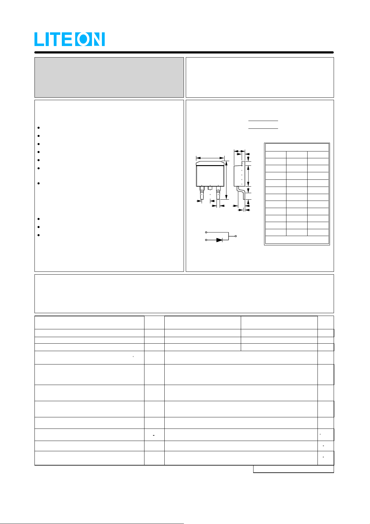
MECHANICAL DATA
Case : D PAK molded plastic
Polarity : As marked on the body
Weight : 0.06 ounces, 1.7 grams
2
REVERSE VOL TAGE
FORWARD CURRENT
2
D PAK
K
A
K
K
12
G
PIN 1
PIN 2
B
E
I
D
C
F
H
J
A
HEATSINK
R
K
- 25 to 30
- 10
DIM.
A
B
C
D
Y
E
F
G
H
I
J
K
All Dimensions in millimeter
Volts
Amperes
2
D PAK
MIN.
9.65 10.69
8.25 9.25
0.51 1.14
2.29
2.29
2.03
1.14
4.37 4.83
MAX.
15.8814.60
1.401.14
2.79
2.79
2.92
1.40
0.640.30
N
I
MAXIMUM RATINGS AND ELECTRICAL CHARACTERISTICS
Ratings at 25℃ ambient temperature unless otherwise specified.
Single phase, half wave, 60HZ, resistive or inductive load.
For capacitive load, der a te c urrent by 20%
L
CHARACTERISTICS
Maximum Repetitive Peak Reverse Voltage
Maximum RM S Voltage
Maximum DC Blocking Voltage
Maximum Average Forward
Rectified Current (See Fig.1)
Peak Forward Surge Current
8.3ms single half sine-wave
superimposed on rated load (JEDEC METHOD)
Maximum Forward
Voltage (Note 1)
Maximum DC Reverse Current
at Rated DC Blocking Voltage
Typical Junction Capacit ance (Note 2 )
Typical Thermal Resistance (Note 3)
Operating Temperature Range
P
@ IF= 10A; TJ =25
@ IF= 10A; TJ =125
@T
C
=
R
@TJ =25
@TJ =100
SYMBOL UNIT
RRM
V
RMS
℃
℃
℃
℃
V
V
I
I
R
DC
(AV)
FSM
V
R
I
C
0JC
T
F
J
J
E
95 C
M
I
SBG1025L
25
17.5
25
10
150
0.45
0.35
5.0
500
350
2.0
-55 to +125
SBG1030L
30
21
30
V
V
V
A
A
V
mA
pF
C/W
C
Storage Temperature Range
NOTES : 1. 300us Pulse Width, 2% Duty Cycle.
2. Measured at 1.0MHz and applied reverse voltage of 4.0V DC.
3.Thermal Resistance Junction to Case.
STG
T
-55 to +150
C
REV. 0-PRE, 10-Jan-2001, KTHB11
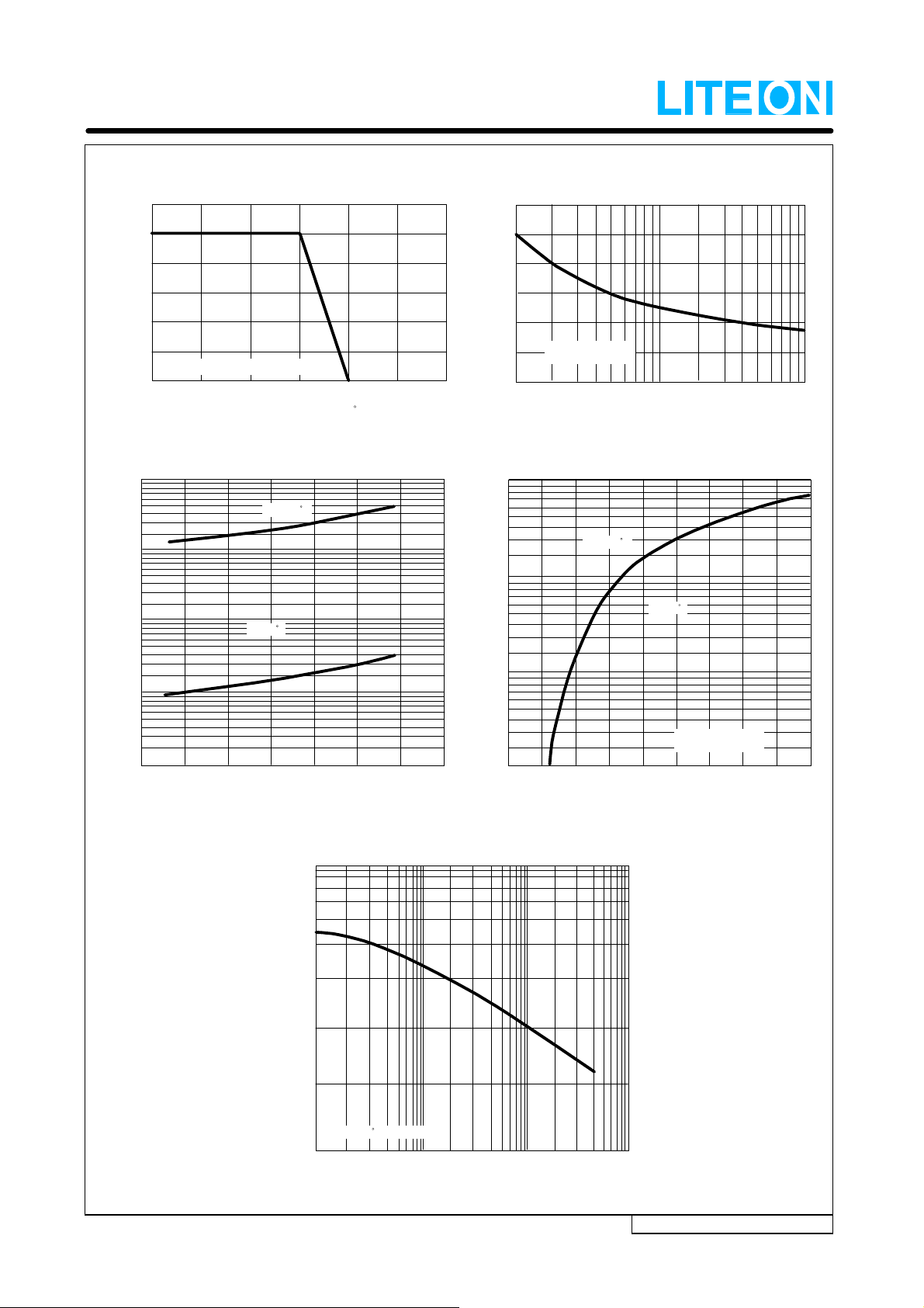
RATING AND CHARACTERISTIC CURVES
SBG1 025L thru SBG1030 L
FIG.1 - FORWARD CURRENT DERATING CURVE
12
8
4
AVERAGE FORWARD CURRENT
AMPERES
100
10
1.0
REVERSE CURRENT ,(mA)
0.1
RESISTIVE OR INDUCTIVE LOAD
0
25
50
FIG.3 - TYPICAL REVERSE CHARACTERISTICS
75 100 125 150
CASE TEMPERATURE , C
TJ= 100 C
TJ= 25 C
175
FIG.2 - MAXIMUM NON-REPETITIVE SURGE CURRENT
175
150
125
100
50
Single Half-Sine-Wave
25
(JEDEC METHOD)
0
PEAK FORWARD SURGE CURRENT,
AMPERES
1 5 10 50 1002
NUMBER OF CYCLES AT 60Hz
FIG.4 - TYPICAL FORWARD CHARACTERISTICS
100
TJ= 125 C
10
A
20
Y
R
TJ= 25 C
N
I
1.0
INSTANTANEOUS FORWARD CURRENT ,(A)
INSTANTANEOUS
0.01
20 40
0
PERCENT OF RATED PEAK REVERSE VOLTAGE, (%)
60 80 100
E
1000
120
L
FIG.5 - TYPICAL JUNCTION CAPACITANCE
M
I
140
0.1
0.1
0.2 0.3
INSTANTANEOUS FORWARD VOLTAGE , VOLTS
0.4 0.5 0.6
PULSE WIDTH 300us
2% Duty Cycle
0.8
0.7
0.9
1.0
R
P
500
CAPACITANCE , (pF)
100
TJ= 25 C, f= 1MHz
0.1
1
REVERSE VOLTAGE , VOLTS
10
4
100
REV. 0-PRE, 10-Jan-2001, KTHB11
 Loading...