

LITEON SB330, SB340, SB320, SB350, SB360 Datasheet
LITE-ON
SEMICONDUCTOR
SB320 thru SB360
SCHOTTKY BARRIER RECTIFIERS
FEATURES
Metal-Semiconductor junction with guard ring
Epitaxial construction
Low forward voltage drop
High current capability
The plastic material carries UL recognition 94V-0
For use in low voltage,high frequency inverters,free
wheeling,and polarity protection applications
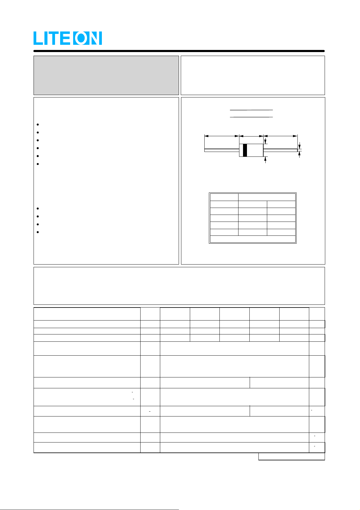
MECHANI CAL DATA
Case : JEDEC DO-201AD molded plastic
Polarity : Color band denotes cathode
Weight : 0.04 ounces, 1.1 grams
Mounting position : Any
REVERSE VOLTAGE
FORWARD CURRENT
DO-201AD
A
Dim.
A
B
C
D
All Dimensions in m illimeter
B
DO-201AD
Min.
25.4
7.30
1.20
4.80 5.30
- 20 to 60
- 3.0
Amperes
A
D
Max.
-
9.50
1.30
Volts
C
MAXIMUM RATINGS AND ELECTRICAL CHARACTERISTICS
Ratings at 25℃ ambient temperature unless otherwise specified.
Single phase, half wave, 60Hz, resistive or inductive load.
For capacitive load, der a te current by 20%
CHARACTERISTICS
Maximum Recurrent Peak Reverse Voltage
Maximum RMS Voltage
Maximum DC Blocking Voltage
Maximum Average Forward Rectified Current
.375",(9.5mm) Lead Lengths (SEE FIG.1)
Peak Forward Surge Current
8.3ms single half sine-wave
super imposed on rated load
Maximum forward Voltage at 3.0A DC
Maximum DC Reverse Current
at Rated DC Blocking Voltage
Typical Thermal Resistance (Note 1)
Typical Junction
Capacitance (Note 2)
Operating Temperature Range
Storage Temperature Range
NOTES : 1.Thermal Resistance Junction to Lead.
2.Measured at 1.0MHz and applied reverse voltage of 4.0V DC.
@TJ =25 C
@TJ =100 C
SYMBOL
RRM
V
RMS
V
DC
V
(AV)
I
FSM
I
F
V
R
I
R
0JL
J
C
J
T
STG
T
SB320
20
14
20
30
21
30
0.50
20
UNIT
mA
C/W
pF
0.74
10
SB360
60
42
60
SB340 SB330
40
28
40
3.0
80
0.5
20
250
-55 to +125
-55 to +150 C
SB350
50
35
50
REV. 2, 01-Dec-2000, KDHF02
V
V
V
A
A
V
C
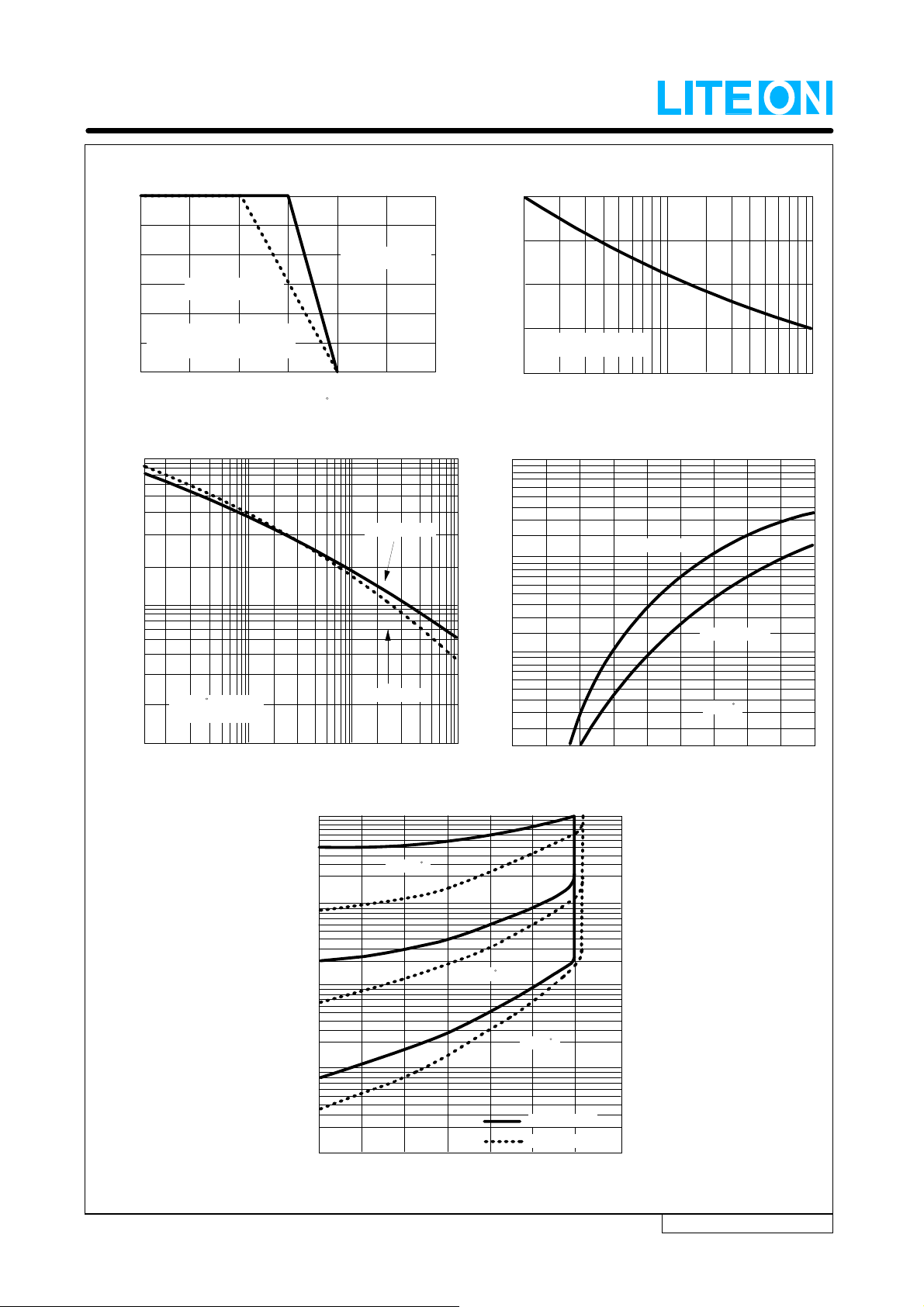
RATING AND CHARACTERISTIC CURVES
SB320 thru SB360
FIG.1 - FORWARD CURRENT DERATING CURVE
3.0
2.0
SB320 thru SB340
1.0
SINGLE PHASE HALF WAVE 60Hz
RESISTI V E OR INDUCT I VE LOAD
0.375" (9.5mm) LEAD LENGTHS
AVERAGE FORWARD CURRENT
AMPERES
0
25
50
75 100 125 150
LEAD TEMPERATURE , C
FIG.3 - TYPICAL JUNCTION CAPACITANCE
1000
100
CAPACITANCE , (pF)
SB350 thru SB360
SB320 to SB340
SB320 to SB340SB320 to SB340SB320 to SB340
175
FIG.2 - MAXIMUM NON-REPETI TIVE SURGE CURRENT
80
60
40
20
Single Half-Sine-Wave
(JEDEC METHOD)
0
PEAK FORWARD SURGE CURRENT,
AMPERES
1
2
510
20
50 100
NUMBER OF CYCLES AT 60Hz
FIG.4 - TYPICAL FORWARD CHARACTERISTICS
100
10
1.0
SB320 to SB340
SB350 to SB360
10
0.1
TJ= 25 C, f= 1MHz
1104
REVERSE VOLTAGE , VOLTS
SB350 to SB360
100
0.1
INSTANTANEOUS FORWARD CURRENT ,(A)
0.1
0.2
0..3
0.4 0.5 0.6
TJ= 25 C
0.7
0.8
0.9
1.0
INSTANTANEOUS FORWARD VOLTAGE , VOLTS
FIG.5 - TYPICAL REVERSE CHARACTERISTIC S
10
TJ= 100 C
1.0
TJ= 75 C
0.1
TJ= 25 C
0.01
INSTANTANEOUS REVERSE CURRENT ,(mA)
SB320 to SB340
0.001
06080100
40
20
PERCENT OF RA TED PEAK REVERSE VOLTAGE (%)
SB350 to SB360
120
140
REV. 2, 01-Dec-2000, KDHF02
 Loading...