

Page 1
6-PIN DIP RANDOM-PHASE
OPTOISOLATORS TRIAC DRIVERS
(600 VOLT PEAK)
MOC3051-M MOC3052-M
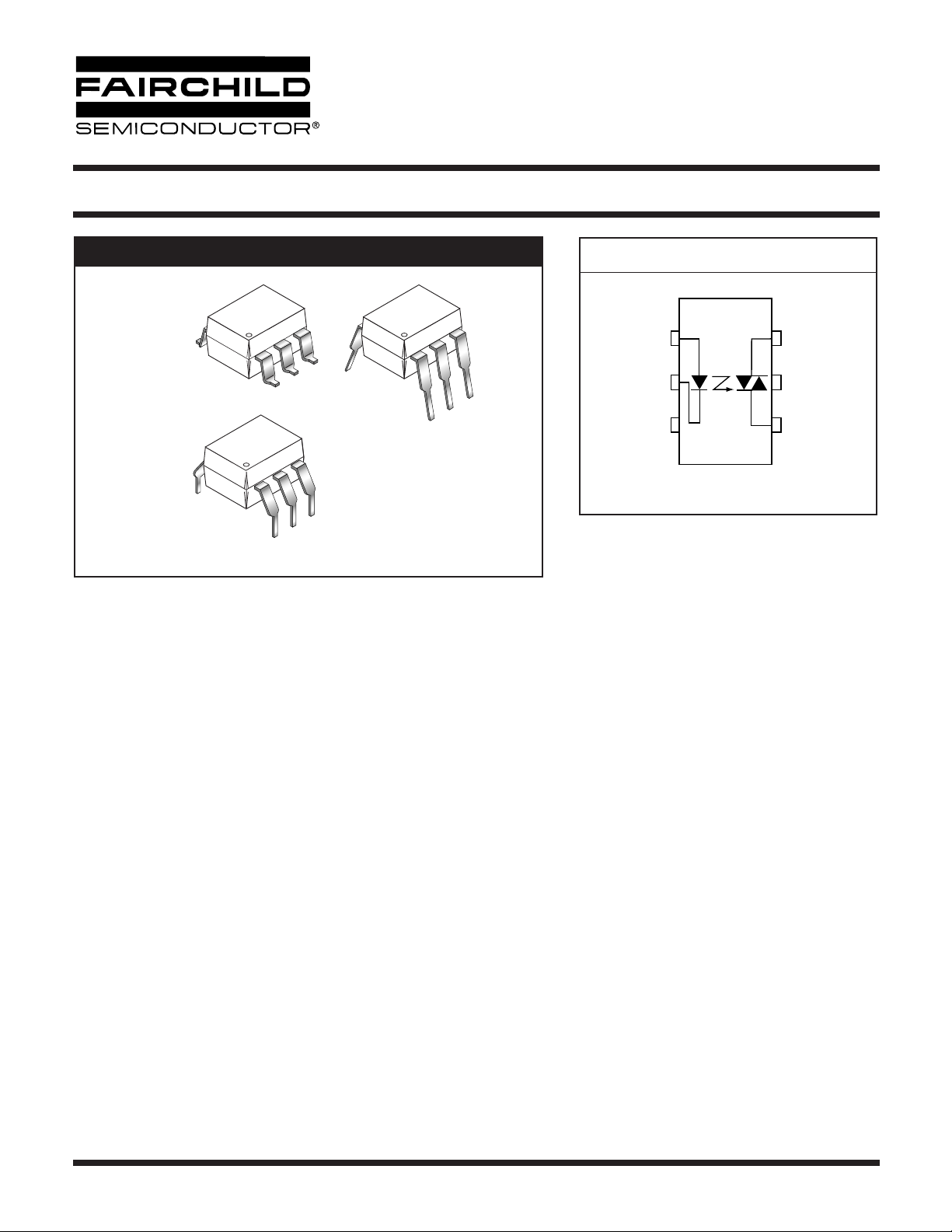
PACKAGE
SCHEMATIC
ANODE
1
MAIN TERM.
6
6
6
CATHODE
2
NC*
5
1
3
1
N/C
*DO NOT CONNECT
(TRIAC SUBSTRATE)
4
MAIN TERM.
6
1
DESCRIPTION
The MOC3051-M and MOC3052-M consist of a AlGaAs infrared emitting diode optically coupled to a non-zero-crossing silicon
bilateral AC switch (triac). These devices isolate low voltage logic from 115 and 240 Vac lines to provide random phase control of
high current triacs or thyristors. These devices feature greatly enhanced static dv/dt capability to ensure stable switching performance of inductive loads.
FEATURES
• Excellent I
• High isolation voltage—minimum 7500 peak VAC
• Underwriters Laboratory (UL) recognized—File #E90700
• 600V peak blocking voltage
• VDE recognized (File #94766)
- Ordering option V (e.g. MOC3052V-M)
stability—IR emitting diode has low degradation
FT
APPLICATIONS
• Solenoid/valve controls
• Lamp ballasts
• Static AC power switch
• Interfacing microprocessors to 115 and 240 Vac peripherals
• Solid state relay
• Incandescent lamp dimmers
•Temperature controls
• Motor controls
© 2005 Fairchild Semiconductor Corporation
Page 1 of 11
6/15/05
Page 2

6-PIN DIP RANDOM-PHASE
OPTOISOLATORS TRIAC DRIVERS
(600 VOLT PEAK)
MOC3051-M MOC3052-M
ABSOLUTE MAXIMUM RATINGS
Parameters Symbol Device Value Units
TOTAL DEVICE
Storage Temperature T
Operating Temperature T
Lead Solder Temperature T
Junction Temperature Range T
(3)
Isolation Surge Voltage
Total Device Power Dissipation @ 25°C
Derate above 25°C 4.4 mW/°C
EMITTER
Continuous Forward Current I
Reverse Voltage V
Total Power Dissipation 25°C Ambient
Derate above 25°C 1.33 mW/°C
DETECTOR
Off-State Output Terminal Voltage V
Peak Repetitive Surge Current (PW = 100 ms, 120 pps) I
Total Power Dissipation @ 25°C Ambient
Derate above 25°C 4 mW/°C
(peak AC voltage, 60Hz, 1 sec duration) V
(T
= 25°C unless otherwise noted)
A
STG
OPR
SOL
J
ISO
P
D
F
R
P
D
DRM
TSM
P
D
All -40 to +150 °C
All -40 to +85 °C
All 260 for 10 sec °C
All -40 to +100 °C
All 7500 Vac(pk)
All
All 60 mA
All 3 V
All
All 600 V
All 1 A
All
330 mW
100 mW
300 mW
© 2005 Fairchild Semiconductor Corporation
Page 2 of 11
6/15/05
Page 3

6-PIN DIP RANDOM-PHASE
OPTOISOLATORS TRIAC DRIVERS
(600 VOLT PEAK)
MOC3051-M MOC3052-M
ELECTRICAL CHARACTERISTICS
(T
= 25°C Unless otherwise specified)
A
INDIVIDUAL COMPONENT CHARACTERISTICS
Parameters Test Conditions Symbol Device Min Typ* Max Units
EMITTER
Input Forward Voltage I
Reverse Leakage Current V
= 10 mA V
F
= 3 V I
R
F
R
DETECTOR
Peak Blocking Current, Either Direction V
Peak On-State Voltage, Either Direction I
Critical Rate of Rise of Off-State Voltage I
TRANSFER CHARACTERISTICS
, I
= 0 (note 1) I
DRM
F
= 100 mA peak, I
TM
= 0 (figure 7, @400V) dv/dt All 1000 V/µs
F
(T
= 25°C Unless otherwise specified.)
A
= 0 V
F
DRM
TM
DC Characteristics Test Conditions Symbol Device Min Typ* Max Units
LED Trigger Current,
either direction
Main terminal
Voltage = 3V (note 2)
Holding Current, Either Direction I
*Typical values at T
= 25°C
A
I
FT
MOC3051-M 15
MOC3052-M 10
H
All 280 µA
Note
1. Test voltage must be applied within dv/dt rating.
2. All devices are guaranteed to trigger at an I
between max 15 mA for MOC3051, 10 mA for MOC3052 and absolute max I
value less than or equal to max I
F
. Therefore, recommended operating I
FT
(60 mA).
F
3. Isolation surge votlage, VISO, is an internal device breakdown rating. For this text, pins 1 and 2 are common, and pins 4, 5 and
6 are common.
All 1.15 1.5 V
All 0.05 100 µA
All 10 100 nA
All 1.7 2.5 V
mA
lies
F
© 2005 Fairchild Semiconductor Corporation
Page 3 of 11
6/15/05
Page 4
0
6-PIN DIP RANDOM-PHASE
OPTOISOLATORS TRIAC DRIVERS
(600 VOLT PEAK)
MOC3051-M MOC3052-M
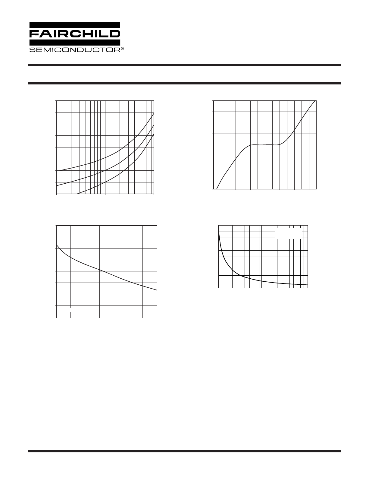
Figure. 1 LED Forward Voltage vs. Forward Current
1.8
1.7
1.6
1.5
1.4
1.3
- FORWARD VOLTAGE (V)
F
V
1.2
1.1
1.0
110100
IF - LED FORWARD CURRENT (mA)
Figure. 3 Trigger Current vs. Ambient Temperature
1.4
1.3
1.2
1.1
(NORMALIZED)
FT
1.0
0.9
0.8
TRIGGER CURRENT - I
0.7
NORMALIZED TO TA = 25°C
0.6
-40 -20 0 20 40 60 80 100
AMBIENT TEMPERATURE - TA (oC)
I
versus Temperature (normalized)
F
TA = -55oC
= 25oC
T
A
= 100oC
T
A
This graph (figure 3) shows the increase of the trigger current
when the device is expected to operate at an ambient temperature below 25°C. Multiply the normalized I
with the data sheet guaranteed I
FT
.
shown this graph
FT
Example:
T
= -40°C, I
A
I
@ -40°C = 10 mA x 1.4 = 14 mA
FT
= 10 mA
FT
Phase Control Considerations
LED Trigger Current versus PW (normalized)
Random Phase Triac drivers are designed to be phase controllable. They may be triggered at any phase angle within the AC
Figure. 2 On-State Characteristics
800
600
400
(mA)
TM
200
0
-200
-400
ON-STATE CURRENT - I
-600
-800
-3 -2 -1 0 1 2 3
ON-STATE VOLTAGE - VTM (V)
Figure. 4 LED Current Required to Trigger vs. LED Pulse Width
25
NORMALIZED TO:
≥
100 µs
20
15
10
5
, NORMALIZED LED TRIGGER CURRENT
FT
I
0
1
251020 50 10
PWin, LED TRIGGER PULSE WIDTH (µs)
PWin
sine wave. Phase control may be accomplished by an AC line
zero cross detector and a variable pulse delay generator which
is synchronized to the zero cross detector. The same task can
be accomplished by a microprocessor which is synchronized
to the AC zero crossing. The phase controlled trigger current
may be a very short pulse which saves energy delivered to the
input LED. LED trigger pulse currents shorter than 100 µs must
have an increased amplitude as shown on Figure 4. This graph
shows the dependency of the trigger current I
versus the
FT
pulse width can be seen on the chart delay t(d) versus the LED
trigger current.
I
in the graph I
FT
minimum specified I
the device characteristic. The normalized I
versus (PW) is normalized in respect to the
FT
for static condition, which is specified in
FT
has to be multi-
FT
plied with the devices guaranteed static trigger current.
Example:
Guaranteed I
I
(pulsed) = 10 mA x 5 = 50 mA
FT
= 10 mA, Trigger pulse width PW = 3 µs
FT
© 2005 Fairchild Semiconductor Corporation
Page 4 of 11
6/15/05
Page 5

6-PIN DIP RANDOM-PHASE
OPTOISOLATORS TRIAC DRIVERS
(600 VOLT PEAK)
MOC3051-M MOC3052-M
Minimum LED Off Time in Phase Control
Applications
AC SINE
ϒ
0
Figure 5. Minimum Time for LED Turn–Off to Zero
180
°
LED PW
LED TURN OFF MIN 200 µs
Cross of AC Trailing Edge
LED CURRENT
In Phase control applications one intends to be able to control
each AC sine half wave from 0 to 180 degrees. Turn on at zero
degrees means full power and turn on at 180 degree means
zero power. This is not quite possible in reality because triac
driver and triac have a fixed turn on time when activated at
zero degrees. At a phase control angle close to 180 degrees
the driver’s turn on pulse at the trailing edge of the AC sine
wave must be limited to end 200 ms before AC zero cross as
shown in Figure 5. This assures that the triac driver has time
to switch off. Shorter times may cause loss of control at the
following half cycle.
Figure. 7 Leakage Current, I
10000
vs. Temperature
DRM
Figure. 6 Holding Current, IH vs. Temperature
1
0.9
0.8
0.7
0.6
0.5
0.4
0.3
0.2
, HOLDING CURRENT (mA)
H
I
0.1
0
-40
-30 -20 -10 0 10 20 30 4050607080
TA, AMBIENT TEMPERATURE (oC)
Figure. 8 LED Trigger Current, IFT vs. dv/dt
1.5
1.4
1.3
1.2
1.1
1
0.9
0.8
0.7
, LED TRIGGER CURRENT (NORMALIZED)
0.6
FT
I
0.5
0.001
0.01 0.1 1 10 100 1000
dv/dt (V/µs)
NORMALIZED TO:
IFT at 3 V
10000
1000
100
10
, LEAKAGE CURRENT (nA)
DRM
I
1
0.1
-40 -20 0 20 40 60 80 100
TA, AMBIENT TEMPERATURE ( o C)
I
versus dv/dt
FT
Tr iac drivers with good noise immunity (dv/dt static) have internal noise rejection circuits which prevent false triggering of the
device in the event of fast raising line voltage transients. Inductive loads generate a commutating dv/dt that may activate the
triac drivers noise suppression circuits. This prevents the
device from turning on at its specified trigger current. It will in
this case go into the mode of “half waving” of the load. Half
waving of the load may destroy the power triac and the load.
Figure 8 shows the dependency of the triac drivers I
versus
FT
the reapplied voltage rise with a Vp of 400 V. This dv/dt condition simulates a worst case commutating dv/dt amplitude.
It can be seen that the I
ing dv/dt reaches 1000 V/ms. The data sheet specified I
does not change until a commutat-
FT
FT
is
therefore applicable for all practical inductive loads and load
factors.
© 2005 Fairchild Semiconductor Corporation
Page 5 of 11
6/15/05
Page 6
2
τ
6-PIN DIP RANDOM-PHASE
OPTOISOLATORS TRIAC DRIVERS
(600 VOLT PEAK)
MOC3051-M MOC3052-M
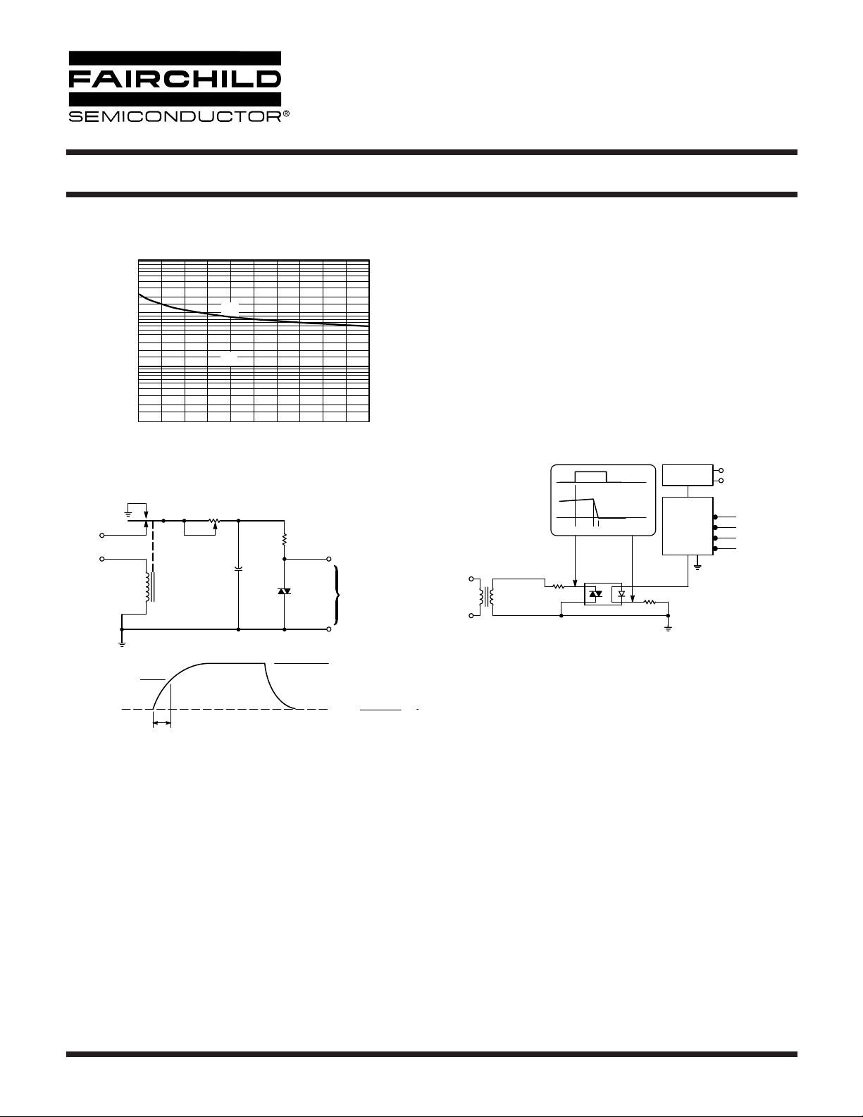
Figure 9. Delay Time, t(d), and Fall T ime, t(f),
100
µ
10
1
t(delay) AND t(fall) ( s)
0.1
10 20 30 40 50 60
+400
Vdc
PULSE
INPUT
MERCURY
vs. LED Trigger Current
t(d)
t(f)
IFT, LED TRIGGER CURRENT (mA)
R
TEST
C
WETTED
RELAY
TEST
D.U.T.
R = 1 k
SCOPE
PROBE
Ω
X100
t(delay), t(f) versus I
FT
The triac driver’s turn on switching speed consists of a turn on
delay time t(d) and a fall time t(f). Figure 9 shows that the delay
time depends on the LED trigger current, while the actual
trigger transition time t(f) stays constant with about one micro
second.
The delay time is important in very short pulsed operation
because it demands a higher trigger current at very short
trigger pulses. This dependency is shown in the graph I
FT
versus LED PW.
The turn on transition time t(f) combined with the power triac’s
turn on time is important to the power dissipation of this
device.
ISOL. TRANSF.
AC
10 k
SCOPE
I
FT
V
TM
t(d)
t(f)
V
TM
DUT
Ω
I
FT
100
Ω
ZERO CROSS
DETECTOR
EXT. SYNC
FUNCTION
GENERATOR
V
out
115 VAC
PHASE CTRL.
PW CTRL.
PERIOD CTRL.
Vo AMPL. CTRL.
APPLIED VOLTAGE
WAVEFORM
0 VOLTS
252 V
τ
RC
Figure 10. Static dv/dt Test Circuit
V
max
dv/dt =
= 400 V
0.63 V
1. The mercury wetted relay provides a high speed repeated
pulse to the D.U.T.
2. 100x scope probes are used, to allow high speeds and
=
τ
RC
voltages.
3. The worst-case condition for static dv/dt is established by
triggering the D.U.T. with a normal LED input current, then
removing the current. The variable R
allows the dv/dt to
TEST
be gradually increased until the D.U.T. continues to trigger
in response to the applied voltage pulse, even after the LED
current has been removed. The dv/dt is then decreased
until the D.U.T. stops triggering. τ
is measured at this
RC
point and recorded.
© 2005 Fairchild Semiconductor Corporation
Page 6 of 11
6/15/05
Page 7
6-PIN DIP RANDOM-PHASE
OPTOISOLATORS TRIAC DRIVERS
(600 VOLT PEAK)
MOC3051-M MOC3052-M
APPLICATIONS GUIDE
Basic Triac Driver Circuit
The new random phase triac driver family MOC3052-M and
MOC3051-M are very immune to static dv/dt which allows
snubberless operations in all applications where external
generated noise in the AC line is below its guaranteed dv/dt
withstand capability. For these applications a snubber circuit is
not necessary when a noise insensitive power triac is used.
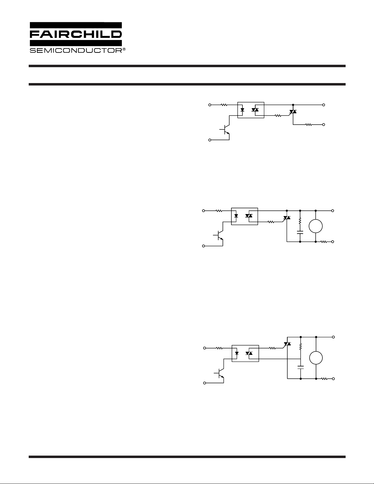
Figure 11 shows the circuit diagram. The triac driver is directly
connected to the triac main terminal 2 and a series Resistor R
which limits the current to the triac driver. Current limiting
resistor R must have a minimum value which restricts the
current into the driver to maximum 1A.
R = Vp AC/I
The power dissipation of this current limiting resistor and the
triac driver is very small because the power triac carries the
load current as soon as the current through driver and current
limiting resistor reaches the trigger current of the power triac.
The switching transition times for the driver is only one micro
second and for power triacs typical four micro seconds.
Triac Driver Circuit for Noisy Environments
When the transient rate of rise and amplitude are expected to
exceed the power triacs and triac drivers maximum ratings a
snubber circuit as shown in Figure 12 is recommended. Fast
transients are slowed by the R-C snubber and excessive
amplitudes are clipped by the Metal Oxide Varistor MOV.
max rep. = Vp AC/1A
TM
LED
Q
TRIAC DRIVER
R
= (VCC - VF LED - V
LED
R = Vp AC line/I
POWER TRIAC
R
TSM
LOAD
sat
Q)/I
AC LINE
FT
V
CC
CONTROL
RET.
R
Figure 11. Basic Driver Circuit
V
CC
CONTROL
RET.
TRIAC DRIVER
R
LED
Typical Snubber values RS = 33 Ω, CS = 0.01 µF
MOV (Metal Oxide Varistor) protects triac and
driver from transient overvoltages >V
POWER TRIAC
R
R
S
C
DRM
S
MOV
max.
AC LINE
LOAD
Figure 12. Triac Driver Circuit for Noisy Environments
Triac Driver Circuit for Extremely Noisy Environments, as
specified in the noise standards IEEE472 and IEC255-4.
Industrial control applications do specify a maximum transient
noise dv/dt and peak voltage which is superimposed onto the
AC line voltage. In order to pass this environment noise test a
modified snubber network as shown in Figure 13 is recommended.
© 2005 Fairchild Semiconductor Corporation
Page 7 of 11
POWER TRIAC
LED
TRIAC DRIVER
R
R
S
MOV
C
S
V
R
CC
CONTROL
RET.
Recommended snubber to pass IEEE472 and IEC255-4 noise tests
RS = 47 W, CS = 0.01 mF
Figure 13. Triac Driver Circuit for Extremely Noisy
Environments
AC LINE
LOAD
6/15/05
Page 8
6-PIN DIP RANDOM-PHASE
)
)
)
)
)
)
OPTOISOLATORS TRIAC DRIVERS
(600 VOLT PEAK)
MOC3051-M MOC3052-M
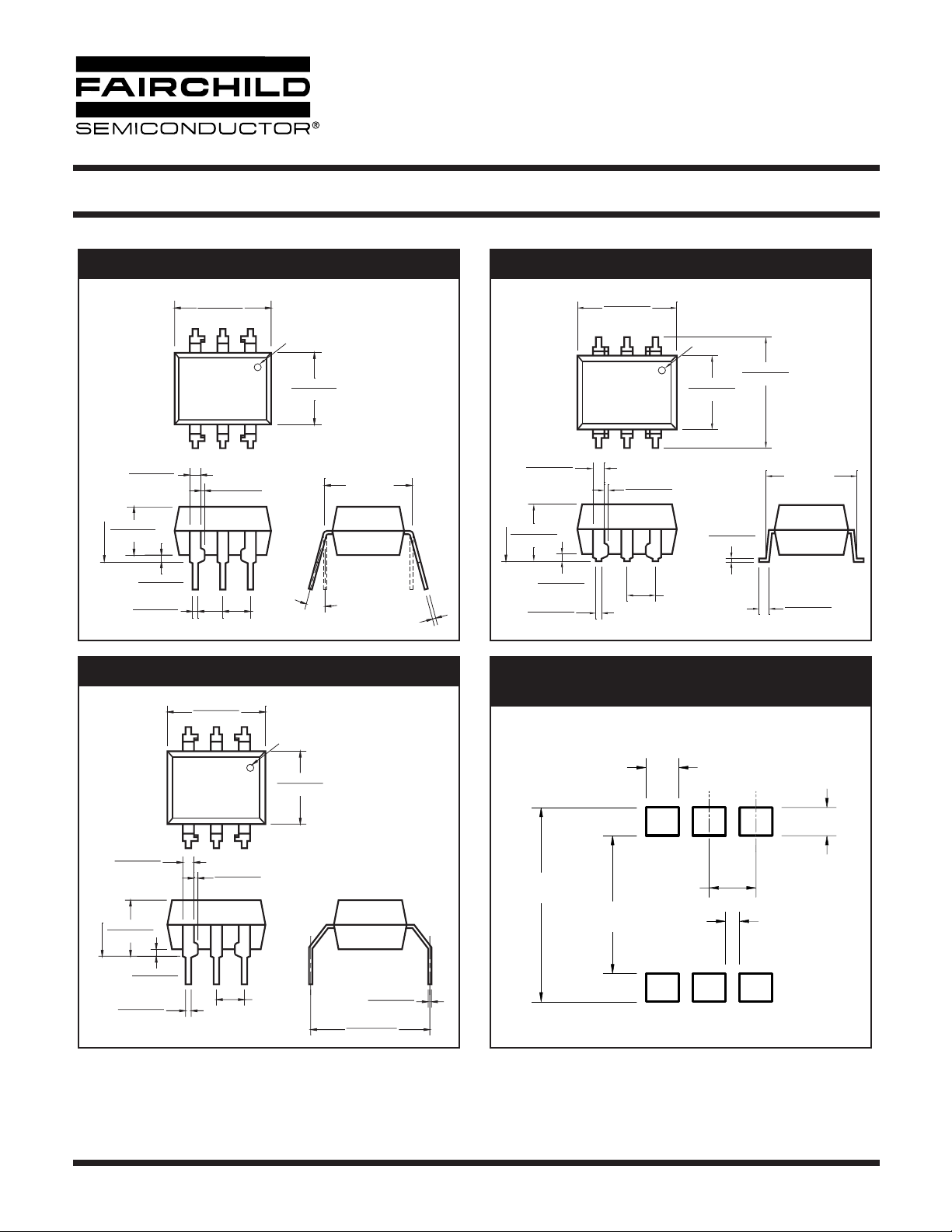
Package Dimensions (Through Hole) Package Dimensions (Surface Mount)
0.350 (8.89)
0.320 (8.13)
0.014 (0.36)
0.010 (0.25)
Pin 1 ID
0.260 (6.60)
0.240 (6.10)
0.100 [2.54]
0.390 (9.90)
0.332 (8.43)
0.012 (0.30)
0.008 (0.20)
0.320 (8.13)
0.035 (0.88)
0.012 (0.30)
0.070 (1.77)
0.040 (1.02)
Seating Plane
0.200 (5.08)
0.115 (2.93)
0.100 (2.54)
0.015 (0.38)
0.020 (0.50)
0.016 (0.41)
0.350 (8.89)
0.320 (8.13)
0.014 (0.36)
0.010 (0.25)
0.100 (2.54)
Pin 1 ID
0.260 (6.60)
0.240 (6.10)
0.320 (8.13)
15°
0.012 (0.30)
0.070 (1.77)
0.040 (1.02)
Seating Plane
0.200 (5.08)
0.115 (2.93)
0.025 (0.63)
0.020 (0.51)
0.020 (0.50)
0.016 (0.41)
Package Dimensions (0.4” Lead Spacing) Recommended Pad Layout for
Surface Mount Leadform
0.350 (8.89)
0.320 (8.13)
Pin 1 ID
0.260 (6.60)
0.240 (6.10)
0.070 (1.77)
0.040 (1.02)
Seating Plane
0.200 (5.08)
0.115 (2.93)
0.100 (2.54)
0.015 (0.38)
0.020 (0.50)
0.016 (0.41)
0.014 (0.36)
0.010 (0.25)
0.100 [2.54]
NOTE
All dimensions are in inches (millimeters)
© 2005 Fairchild Semiconductor Corporation
0.012 (0.30)
0.008 (0.21)
0.425 (10.80)
0.400 (10.16)
Page 8 of 11
0.425 (10.79
0.100 (2.54
0.305 (7.75
0.070 (1.78
0.060 (1.52
0.030 (0.76
6/15/05
Page 9
6-PIN DIP RANDOM-PHASE
OPTOISOLATORS TRIAC DRIVERS
(600 VOLT PEAK)
MOC3051-M MOC3052-M
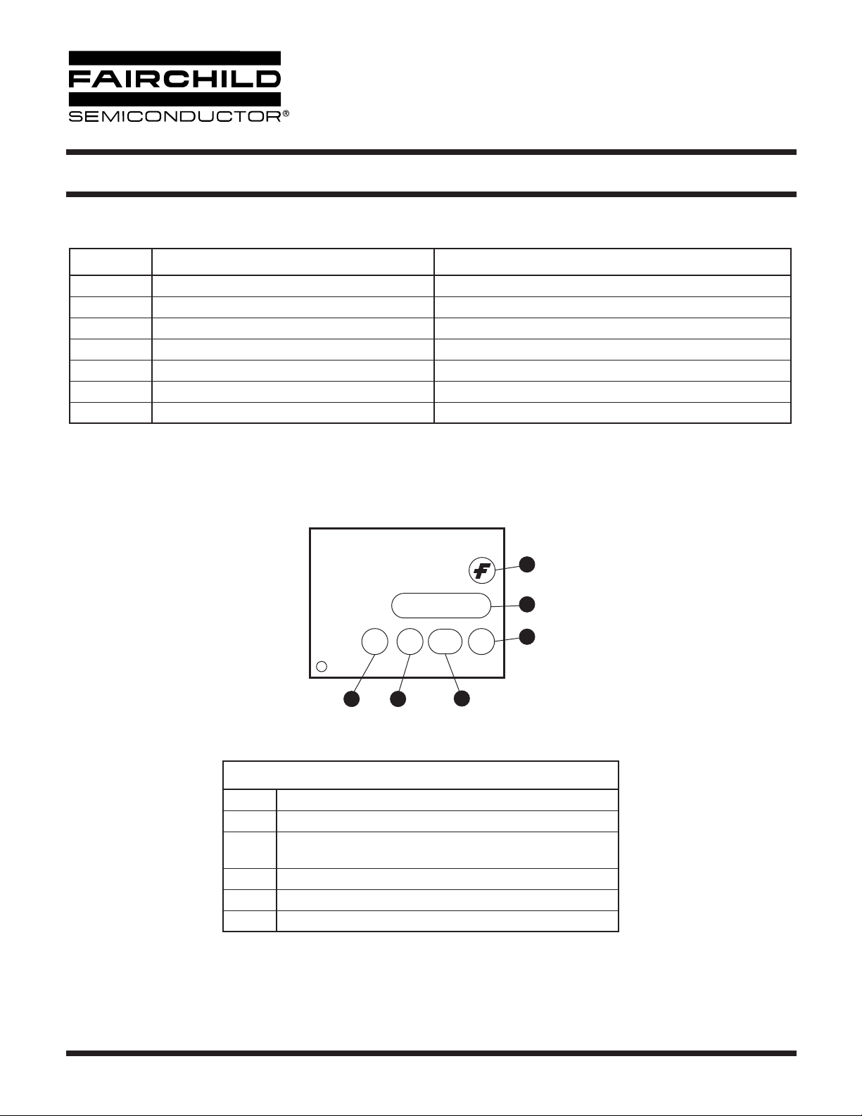
ORDERING INFORMATION
Option Order Entry Identifier Description
SSSurface Mount Lead Bend
SD SR2 Surface Mount; Tape and reel
WT0.4" Lead Spacing
300 V VDE 0884
300W TV VDE 0884, 0.4" Lead Spacing
3S SR2V VDE 0884, Surface Mount
3SD SR2V VDE 0884, Surface Mount, Tape & Reel
MARKING INFORMATION
1
MOC3051
V X YY Q
43
Definitions
1Fairchild logo
2Device number
VDE mark (Note: Only appears on parts ordered with VDE
3
option – See order entry table)
4 One digit year code, e.g., ‘3’
5Two digit work week ranging from ‘01’ to ‘53’
6 Assembly package code
*Note – Parts that do not have the ‘V’ option (see definition 3 above) that are marked with
date code ‘325’ or earlier are marked in portrait format.
5
2
6
© 2005 Fairchild Semiconductor Corporation
Page 9 of 11
6/15/05
Page 10
6-PIN DIP RANDOM-PHASE
OPTOISOLATORS TRIAC DRIVERS
(600 VOLT PEAK)
MOC3051-M MOC3052-M
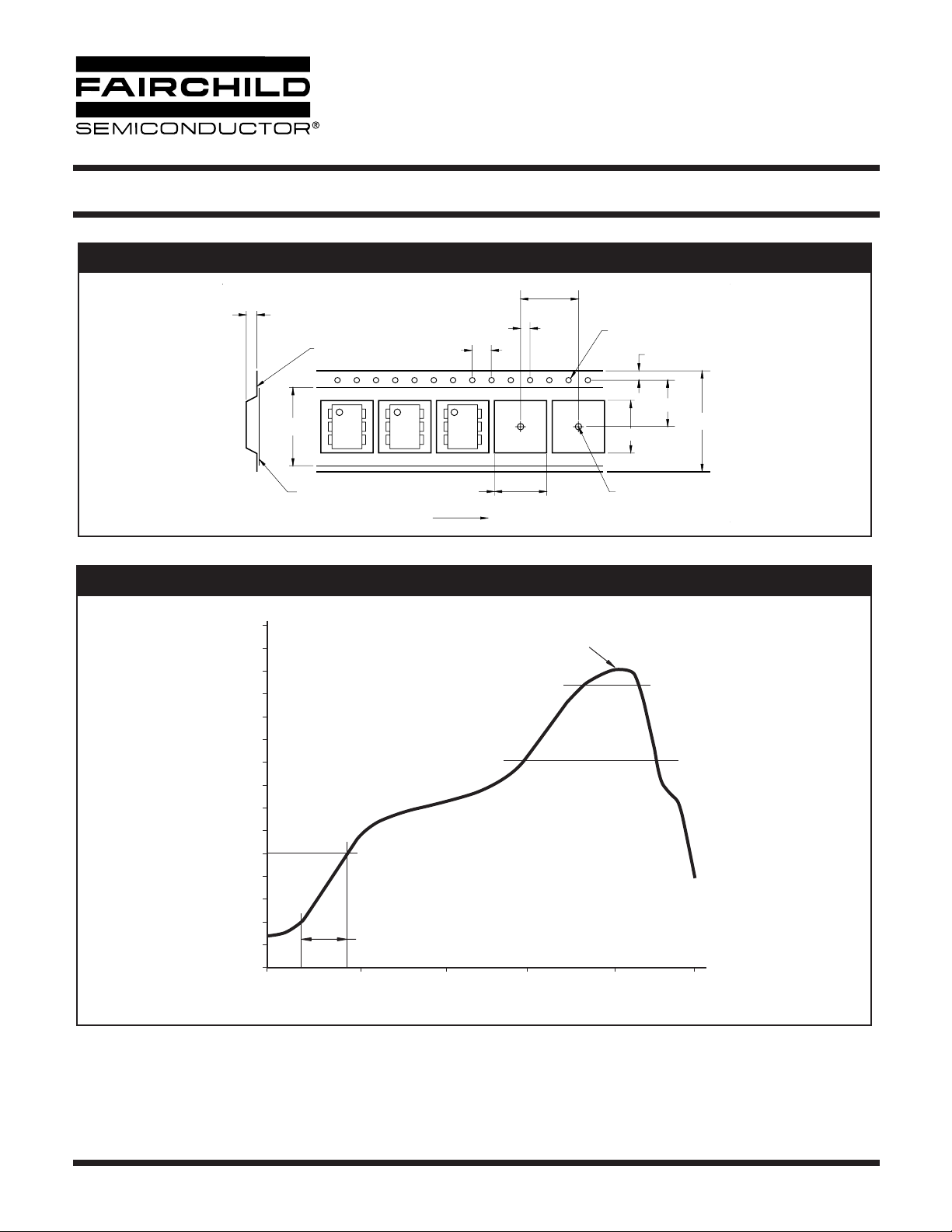
Carrier Tape Specifications
4.5 ± 0.20
0.30 ± 0.05
21.0 ± 0.1
0.1 MAX
User Direction of Feed
Reflow Profile (White Package, -M Suffix)
300
280
260
240
220
200
180
160
°C
140
120
100
80
60
40
20
0
0 60 180120 270
12.0 ± 0.1
2.0 ± 0.05
4.0 ± 0.1
10.1 ± 0.20
1.822°C/Sec Ramp up rate
33 Sec
Time (s)
1.5 MIN
Ø
9.1 ± 0.20
260°C
Time above
183°C = 90 Sec
1.75 ± 0.10
11.5 ± 1.0
24.0 ± 0.3
Ø
1.5 ± 0.1/-0
>245°C = 42 Sec
360
© 2005 Fairchild Semiconductor Corporation
Page 10 of 11
6/15/05
Page 11

6-PIN DIP RANDOM-PHASE
OPTOISOLATORS TRIAC DRIVERS
(600 VOLT PEAK)
MOC3051-M MOC3052-M
DISCLAIMER
FAIRCHILD SEMICONDUCTOR RESERVES THE RIGHT TO MAKE CHANGES WITHOUT FURTHER NOTICE TO
ANY PRODUCTS HEREIN TO IMPROVE RELIABILITY, FUNCTION OR DESIGN. FAIRCHILD DOES NOT ASSUME
ANY LIABILITY ARISING OUT OF THE APPLICATION OR USE OF ANY PRODUCT OR CIRCUIT DESCRIBED HEREIN;
NEITHER DOES IT CONVEY ANY LICENSE UNDER ITS PATENT RIGHTS, NOR THE RIGHTS OF OTHERS.
LIFE SUPPORT POLICY
FAIRCHILD’S PRODUCTS ARE NOT AUTHORIZED FOR USE AS CRITICAL COMPONENTS IN LIFE SUPPORT DEVICES
OR SYSTEMS WITHOUT THE EXPRESS WRITTEN APPROVAL OF THE PRESIDENT OF FAIRCHILD SEMICONDUCTOR
CORPORATION. As used herein:
1. Life support devices or systems are devices or systems
which, (a) are intended for surgical implant into the body, or
(b) support or sustain life, and (c) whose failure to perform
when properly used in accordance with instructions for use
provided in the labeling, can be reasonably expected to
result in a significant injury of the user.
2. A critical component in any component of a life support
device or system whose failure to perform can be
reasonably expected to cause the failure of the life support
device or system, or to affect its safety or effectiveness.
© 2005 Fairchild Semiconductor Corporation
Page 11 of 11
6/15/05
 Loading...