

LITEON MBR870, MBR890, MBR8100, MBR880 Datasheet
LITE-ON
SEMICONDUCTOR
MBR870 thru MBR8100
SCHOTTKY BARRIER RECTIFIERS
FEATURES
Metal of silicon rectifier,majority carrier conducton
Guard ring for transient pro tec tio n
Low power loss, high efficiency
High current capability, low VF
High surge capacity
Plastic package has UL flammability classification 94V-0
For use in low voltage,high frequency inv erters,free
whelling,and polarity protection applications
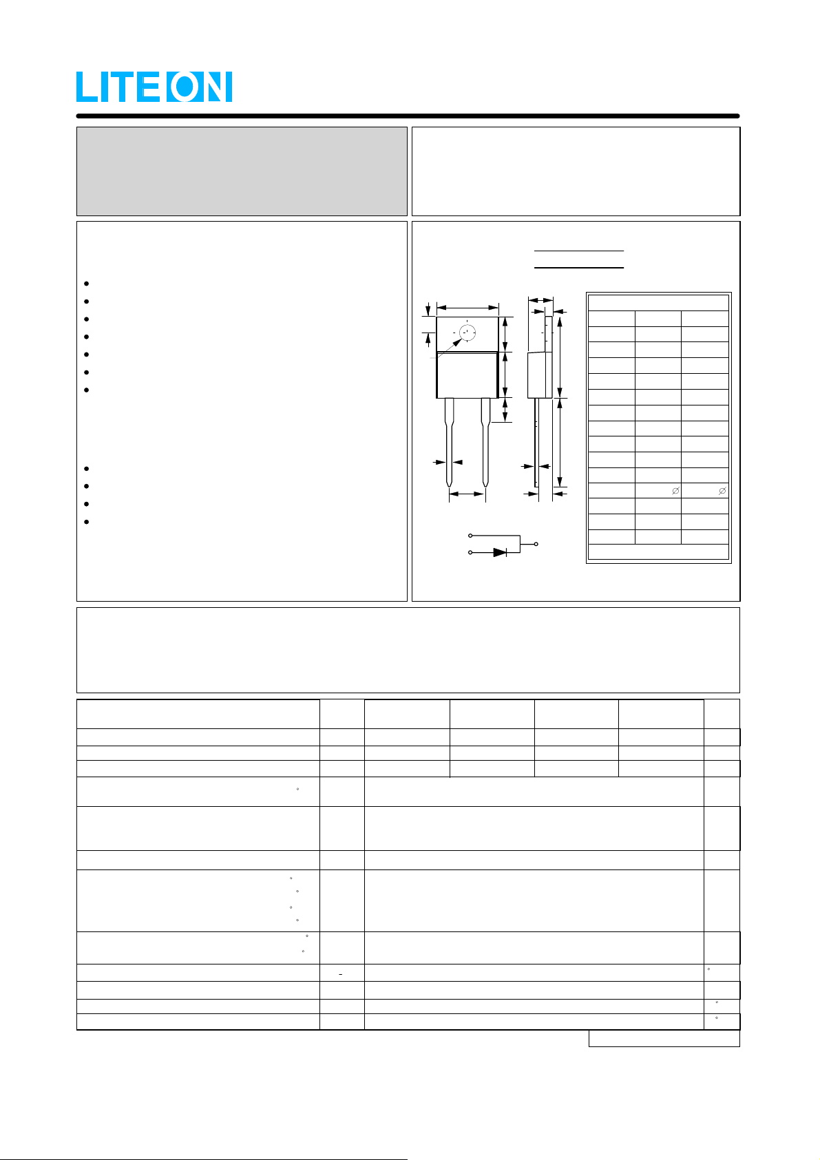
MECHANICAL DATA
Case : TO-220AC molded plastic
Polarity : As marked on the body
Weight : 0.08 ounces, 2.24 grams
Mounting position : Any
REVERSE VOLTAGE
FORWARD CURRENT
TO-220AC
C
K
12
I
PIN 1
PIN 2
B
PIN
H
L
D
E
F
J
M
A
G
N
CASE
- 70 to 100
- 8.0
Amperes
TO-220AC
DIM.
A
B
C
D
E
F
G
H
I
J
K
L
M
N
All Dimensions in millimeter
Volts
MIN.
14.22 15.88
9.65
2.54
5.84
8.26
-
12.70
4.83
0.51
3.53 4.09
3.56 4.83
1.14 1.40
2.03
MAX.
10.67
3.43
6.86
9.28
6.35
14.73
5.33
1.14
0.64 0.30
2.92
MAXIMUM RATINGS AND ELECTRICAL CHA RACTERISTICS
Ratings at 25℃ ambient temperature unless otherwise specified.
Single phase, half wave, 60Hz, resistive or inductive load.
For capacitive load, derate current by 20%
CHARACTERISTICS
Maximum Recurrent Peak Reverse Voltage
Maximum RMS Voltage
Maximum DC Blocking Voltage
Maximum Average Forward
Rectified Current (See Fig.1)
Peak Forward Surge Current
8.3ms single half sine-wave
superimposed on rated load (JEDEC METHOD)
Voltage Rate of Change (Rated VR )
F
Maximum Forward
Voltage (Note 1)
Maximum DC Reverse Current
at Rated DC Blocking Voltage
Typical Thermal Resistance (Note 2)
Typical Junction Capacitance (Note 3)
Operating Temperature Range
Storage Temperature Range
I
F
I
F
I
F
I
=8A @
=8A @
=16A @
=16A @
@T
110 C
C
=
TJ =25 C
TJ =125 C
TJ =25 C
TJ =125 C
@TJ =25 C
@TJ =125 C
NOTES : 1. 300us Pulse Width, Duty Cycle 2%
2. Thermal Resistance Junction to Case.
3. Measured at 1.0MHz and Applied Reverse Voltage of 4.0V DC.
SYMBOL
RRM
V
RMS
V
DC
V
(AV)
I
FSM
I
dv/dt
F
V
R
I
R
0JC
J
C
J
T
STG
T
MBR870 MBR880
MBR870
MBR870MBR870
70
49
70
80
56
80
8
125
10000
0.85
0.75
0.95
0.85
0.1
100
2.0
280
-55 to +150
-55 to +175
MBR890
90
MBR8100
100
63
90
REV . 3, 13-S e p-2001 , K T H A09
100
70
UNIT
V
V
V
A
A
V/us
V
mA
C/W
pF
C
C
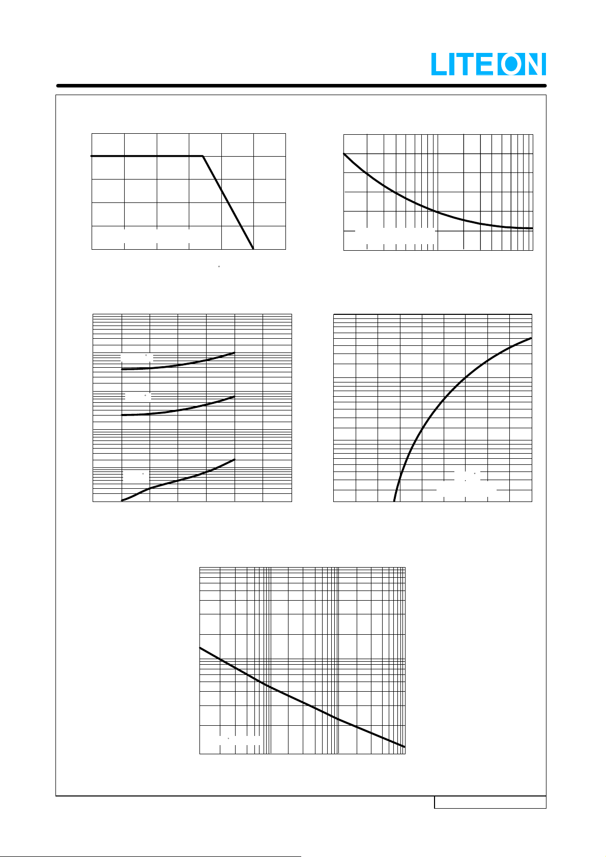
RATING AND CHARA CTERISTIC CURVES
MBR870 thru MBR8100
FIG.1 - FORWARD CURRENT DERATING CURVE
10
8
6
4
2
AVERAGE FORWARD CURRENT
AMPERES
RESISTIVE OR INDUCTIVE LOAD
0
0
25
50
75 100 125 150
CASE TEMPERATURE , C
FIG.3 - TYPICAL REVERSE CHARACTERISTICS
100
10
1
TJ= 125 C
TJ= 75 C
175
FIG.2 - MAXIMUM NON-REPETITIVE SURGE CURRENT
150
125
100
75
50
25
8.3ms Single Half-Sine-Wave
(JEDEC METHOD)
0
PEAK FORWARD SURGE CURRENT,
AMPERES
1 5 10 50 1002
20
NUMBE R OF CYCLES A T 60Hz
FIG.4 - TYPICAL FORWARD CHARACTERISTICS
100
100
10
10
REVERSE CURRENT ,(mA)
0.1
0.01
INSTANTANEOUS
0.001
0
TJ= 25 C
20 40
60 80 100
PERCENT OF RA TED PEAK REVERSE VOLTAGE ,(%)
10000
1000
CAPACITANCE , (pF)
1.0
1.0
INSTANTANEOUS FORWARD CURRENT ,(A)
INSTANTANEOUS FORWARD CURRENT ,(A)
0.1
120
140
0.1
0.2 0.3
0.1
INSTANTANEOUS FORWARD VOLTAGE , VOLTS
INSTANTANEOUS FORWARD VOLTAGE , VOLTS
FIG.5 - TYPICAL JUNCTION CAPACITANCE
PULSE WIDTH 300ua
PULSE WIDTH 300us
2% Duty cycle
0.4 0.5 0.6
TJ= 25 C
0.7
0.8
0.9
1.0
TJ= 25 C, f= 1MHz
100
0.1
1
10
4
REVERS E VOLTAGE , VO LTS
100
REV. 3, 13 -S ep -20 0 1, KT HA09
 Loading...