

Page 1

Service Manual
15-inch LCD Monitor
EC150ATA
Page 2

EC-150ATA
Table of Contents
1. Audio circuit --------------------------------------------------------------------------------------------------------------- 1
1.1 Audio input ------------------------------------------------------------------------------------------------------------ 1
1.2 Audio output ---------------------------------------------------------------------------------------------------------- 1
2. Power supply -------------------------------------------------------------------------------------------------------------- 1
3. On-screen circuit ---------------------------------------------------------------------------------------------------------- 1
4. Video input circuit -------------------------------------------------------------------------------------------------------- 1
5. Definition converter LSI peripheral circuit ---------------------------------------------------------------------------- 1
6. System reset, LED control circuit --------------------------------------------------------------------------------------- 2
7. E2PROM for PNP --------------------------------------------------------------------------------------------------------- 2
8. E2PROM -------------------------------------------------------------------------------------------------------------------- 2
9. CPU circuit ----------------------------------------------------------------------------------------------------------------- 2
9.1 Dection of POWER switch status ---------------------------------------------------------------------------------- 2
9.2 Display mode identification ----------------------------------------------------------------------------------------- 2
9.3 User control ----------------------------------------------------------------------------------------------------------- 4
9.4 Control of identification converter LSI (IC 14) ------------------------------------------------------------------ 5
9.5 I2C bus control -------------------------------------------------------------------------------------------------------- 5
9.6 Power ON sequence -------------------------------------------------------------------------------------------------- 6
9.7 Power OFF sequence ------------------------------------------------------------------------------------------------- 7
9.8 List of CPU assignments--------------------------------------------------------------------------------------------- 8
10. Inverter Protective circuit for back light ------------------------------------------------------------------------------- 9
11. USB circuit -----------------------------------------------------------------------------------------------------------------9
11.1 3.3V cutoff circuit for USB identification ----------------------------------------------------------------------- 9
11.2 USB hub control circuit -------------------------------------------------------------------------------------------- 9
11.1 Lower port circuit --------------------------------------------------------------------------------------------------- 9
11.1 DC/DC converter circuit ------------------------------------------------------------------------------------------------- 9
IndexCircuit Description
Page 3

EC-150ATA
1. Audio circuit (Circuit diagrams Main PWB 1/1 JACK PWB 1/1)
1.1 Audio input
The audio signal input received from the audio input terminal (JK011) is applied to the pre-amplifier I006 of 2
(L-CH) and 3 (R-CH) through the low-pass filter consisting of R047, R049, R048, R050, C013 and C014.
In this pre-amplifier, controls of Volume, Balance, Bass, and Treble are conducted. The audio signal controlled
at the pre-amplifier is entered in and amplified at the AMF I007 of 2 (L-CH) and 1 (R-CH). Since then, the signal
is output to the jack board through a cable.
1.2 Audio output
The audio signal is output from the head-phone output terminal (JK001) of the jack board to the speaker system
or the head-phone.
When the stereo mini-plug is inserted in the head-phone output terminal, output from the speaker is suspended,
but the audio signal attenuated by resistors R001 and R002 is output to the stereo mini-plug side.
2. Power supply (Circuit daigrams MAIN PWB 7/8)
1. I314:DC-DC converter
A 5V power supply for LCD module, CPU, and logic is generated from the 12V source.
2. I315:3-terminal regulator
A 3.3V power supply for LCD module is generated from the 5V source.
3. I315:3-terminal regulator
A 3.3V power supply for I317 analog is generated from the 5V source.
4. I315:3-terminal regulator
A 3.3V power supply for I317 digital is generated from the 5V source.
Q303, I312 ON/OFF control for LCD Module
ON/OFF control is performed for power ON/OFF and also for the power saving sequence.
3. On-screen circuit (Circuit diagrams Main PWB 3/8)
I310 (MTV130P-30) is an OSD IC.
The HREF Signal, the OSDVS signal (horizontal / vertical sync signal in negative polarity), and the OSDTCLK
signal (dot clock for OSD display) are received from I317 (Circuit diagram MAIN PWB 3/8 gmZAN1), and the
OSD functions controlled by IIC interface (pin 7, pin 8).
Using these data, and On-screen menu screen is established and the resultant data are output to I317 (Circuit
diagram MAIN PWB 3/8, gmZAN1).
4. Video input circuit (Circuit diagram MAIN PWB 4/8)
The AC-coupled video signal is used to clamp the black level at 0V).
5. Definition converter LSI peripheral circuit (Circuit diagram MAIN PWB)
I317 gmZAN1 is the definition converter LSI.
The analog R, G, B signal input entered from the video input circuit is converted into the digital data of video
signal through the incorporated A/D converter. Based on this conversion, this device performs interpolation
during pixel extension. The source voltage for this device is 3.3V and the system clock frequency is 50MHz.
The withstand voltage level for the input signal voltage if I317 is 3.3V and 5V.
Page 1Circuit Description
Page 4

EC-150ATA
6. System reset, LED control circuit (Circuit diagram MAIN PWB 2/8, 3/8)
6.1 System reset
System reset is performed by detecting the rising and falling of the 5V source voltage at I301.
6.2 LED control circuit
Green / amber is lit with the control signal of the LED GREEN and LED AMBER signal pin 15, 12 from I307
(Circuit diagram MAIN PWB 2/8).
7. E2PROM for PnP (Circuit diagram MAIN PWB 2/8)
8. E2PROM (Circuit diagram MAIN PWB 2/8)
Data transfer between I305 (AT24 C16) and CPU (Circuit diagram MAIN PWB 2/8 (I302) is effected through
the IIC bus SCL (pin 15) and SDA (pin 16) of I302. The data to be transferred to each device are stored in I305.
l I317 control data.
l OSD related setting data.
l Other control data for service menu.
9. CPU circuit (Circuit diagram MAIN PWB 2/8)
I302 (80C51RA2) functions as the CPU.
The source voltage for the device is 5.0V and the system clock frequency is 20MHz.
9.1 Detection of POWER switch status
The CPU identifies the ON status of the two power supplies. The identification is made when the power supply
is turned off. For example, if the power supply is turned off with the POWER switch, the POWER switch must be
turned on when activating the power supply again. If the power supply is turned off by pulling out the power
cord, then this power supply can be turned on by connecting the power cord, without pressing the POWER
switch.
9.2 Display mode identification
9.2.1 Functions
(1) Display mode identification
l The display mode of input signal is identified based on Table 1, and according to the frequency and polarity
(HPOL, VPOL) of horizontal or vertical sync signal, presence of the horizontal or vertical sync signal, and the
discrimination signal (HSYNC_DETECT, VSYNC_DETECT).
l In MOD [3] [4], inappropriate polarity, composite sync, and sync ON green are indentified as MOD [4].
l When the mode has been identified through the measurement of horizontal and vertical frequencies, the total
number of lines is determined with a formula of Horizontal frequency / Vertical frequency = Total number
of lines. Final identification can be made by examining the coincidence of the obtained figure with the
number of lines for the mode identified from the frequency. The boundary number of lines in each mode is
shown in Table 2.
l When the detected frequency if the sync signal has changed, the total number of lines should be counted even
through it is rge identified frequency in the same mode. Then, it is necessary to examine whether the preset
value for the vertical display position of Item 4-3 has exceeded the total number of lines. If exceeded, a
maximum value should be set up, which does not exceed the vertical display position of Item 4-3.
(2) Power save mode.
This power save mode is assumed when the frequency of the horizontal / vertical signal is as specified below.
l Vertical frequency : Below 24 KHz
l Horizontal frequency : 75 KHz or above,
l VTOTAL : 1027 or more.
Page 2 Circuit Description
Page 5
EC-150ATA
q
y
y
y
)
)
)
)
)
)
)
)
)
)
)
)
)
)
)
(3) Asset management
As an action for asset management, the potential at the WRITE PROTECT pin is turned to be H if there is a
vertical input of vertical frequency (42 Hz +/- 1 Hz),
For more detailed setting method, refer to 4-6-5-14 (8). During this operation, this system stays in the Out-OfRange mode.
(4) Power save mode.
The power save mode is assumed when the horizontal / vertical signals are as specified below.
l If there is no horizontal sync signal input.
l If there is no vertical sync signal input.
l If the horizontal sync signal is outside the measuring range of gmZAN1.
l If the vertical sync signal is outside the measuring range of gmZAN1.
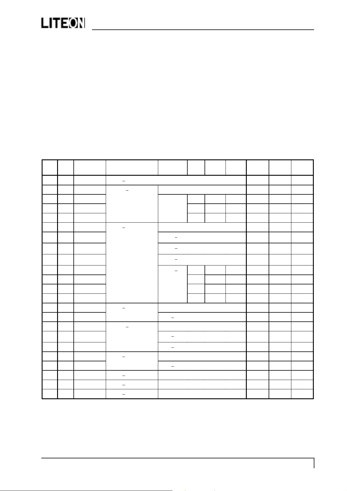
Table 1
Signal
Preset Mode HSYNC: Frequency VSYNC:
No.
1 640 x 400 (56)24 KHz < fH < 30.8 KHz 21.053 24.830 56.432
2 640 x 480 (60)30.8 KHz < fH < 33 KHz FV < 63 Hz 25.175 31.469 59.992
3 720 x 350 (70
4 720 x 400 (70
4 720 x 400 (70
5 800 x 600 (56)33 KHz < fH < 43 KHz FV < 58 Hz 36.000 35.156 56.250
6 800 x 600 (60
7 640 x 480 (66
8 640 x 480 (72
9 640 x 480 (75
10 720 x 350 (85
11 720 x 400 (85
11 720 x 400 (85
12 800 x 600 (75)43 KHz < fFH < 47.2 KHz FV < 80 Hz 49.500 46.875 75.000
13 640 x 480 (85
14 1024 x 768 (60)47.2 KHz < fH < 51 KHz FV < 63 Hz 65.000 48.363 60.004
15 800 x 600 (72
16 832 x 624 (75
14 1024 x 768 (60)51 KHz < fH < 55 KHz FV < 70 Hz 70.490 52.448 60.004
17 800 x 600 (85
18 1024 x 768 (70)55 KHz < fH < 59 KHz 75.000 56.476 70.069
19 1024 x 768 (75)59 KHz < fH < 62 KHz 78.750 60.023 75.029
20 1024 x 768 (85)62 KHz < fH < 75 KHz 94.500 68.677 84.977
Fre
uenc
58 KHz < fV<
63 KHz
63 KHz < fV<
68 KHz
68 KHz < fV<
74 KHz
74 KHz < fV SEP - - 31.500 37.500 75.000
80 Hz < fV 36.000 43.269 85.008
63 Hz < fV <
73 Hz
73 Hz < fV 57.283 49.725 74.550
70 Hz < fV 56.250 53.674 85.061
SYNC
HSYNC:
TYPE
OTHER OTHER OTHER
OTHER OTHER OTHER
Polarit
SEP + - 25.175 31.469 70.087
SEP - + 25.175 31.469 70.087
SEP + - 31.500 37.861 85.080
SEP - + 31.500 37.861 85.080
VSYNC:
Polarit
DOTCLK fH(KHz)FV (Hz
40.000 37.879 60.317
30.240 35.000 66.611
31.500 37.861 72.809
50.000 48.077 72.188
Page 3Circuit Description
Page 6
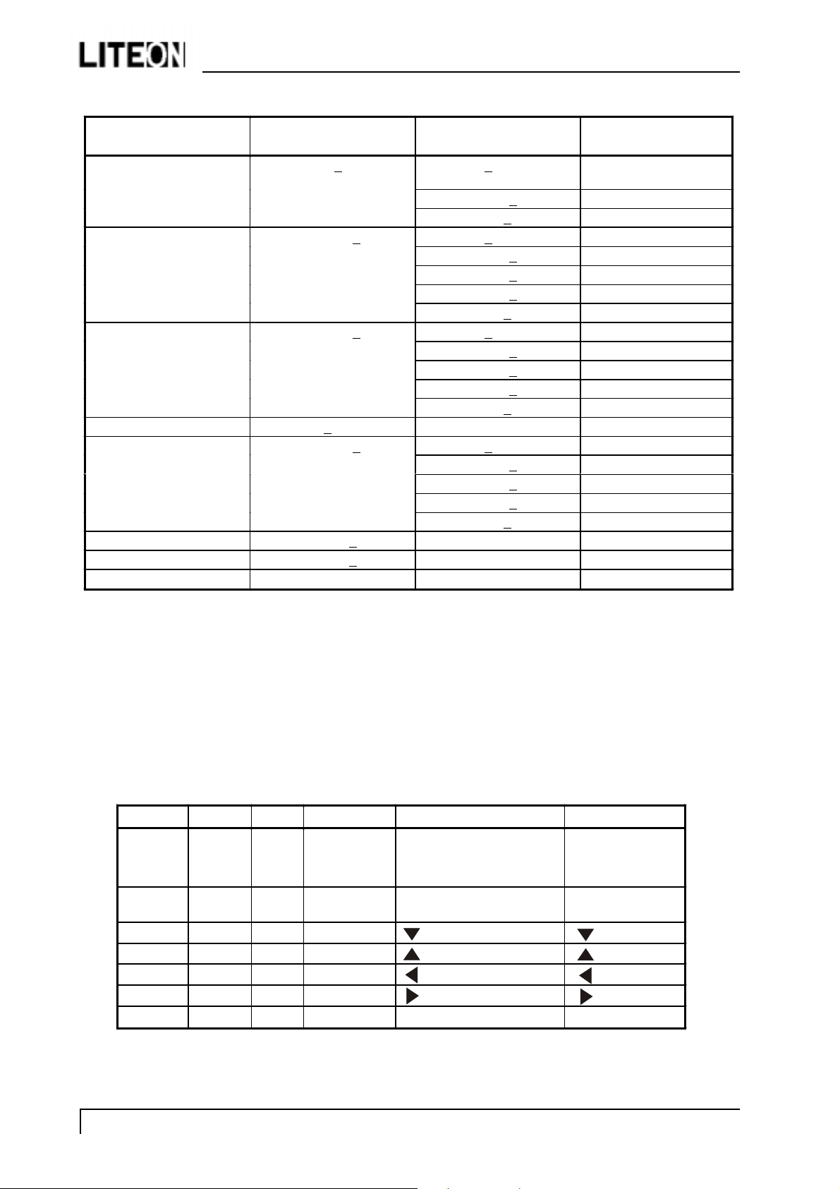
Table 2 the number of the lines, Vsync distinction
EC-150ATA
Indication resolution The number of the
distinction lines
The mode of 400 line and
under
640 x 480 487 < LINE < 607 fV < 63 Hz 6
800 x 600 607 < LINE < 777 fV < 58 Hz 11
832 x 624 640 < LINE -16
1024 x 768 768 < LINE < 870 fV < 63 Hz 17
1152 x 864 870 < LINE < 1031 UN SUPPORT
1280 x 960 960 < LINE < 1027 UN SUPPORT
1280 x 1024 1027 < LINE UN SUPPORT
LINE < 487 fV < 63 Hz 3
Distinction Vsync The fixed mode
63 Hz < fV < 78 Hz 1
78 Hz < fV 11
63 Hz < fV < 68 Hz 7
68 Hz < fV < 74 Hz 8
74 Hz < fV < 78 Hz 9
78 Hz < fV 10
58 Hz < fV < 63 Hz 12
63 Hz < fV < 73 Hz 14
73 Hz < fV < 78 Hz 13
78 Hz < fV 15
63 Hz < fV < 68 Hz 18
68 Hz < fV < 73 Hz 19
73 Hz < fV < 78 Hz 20
78 Hz < fV 21
Attention :
1. Make it the mode 16 by the first HSYNC, the VSYNC distinction in the time beyond 640 line when you
recognize it with the mode 16.
2. When resolution beyond 1024 x 768 is inputted, resolution is lowered with Down scaling to 1024 x 768, and
indicated, and OSD should indicate OUT of Range.
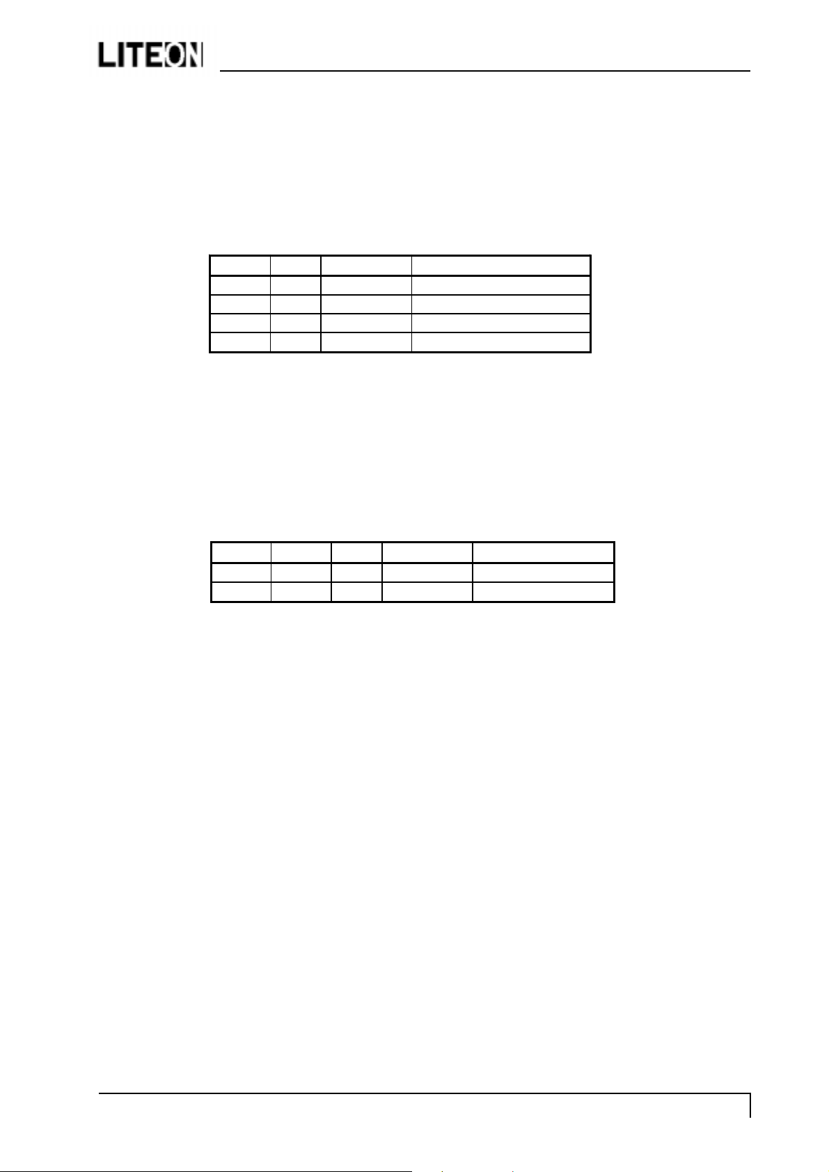
9.3 User Control
9.3.1 Related ports of I317
Port Pin No. I/O Signal name Function Remarks
MFB1 112 1 RESET RESET switch input The set value is
returned to the
initial value
MFB5 107 1 EXIT EXIT switch input Withdraw from
OSD
MFB10 124 1 DOWN switch input ( ) key
MFB4 109 1 UP switch input ( ) key
MFB11 123 1 - switch input ( ) key
MFB3 110 1 + switch input ( ) key
MFB2 111 1 PROCEED PROCEED switch input Functional
Page 4 Circuit Description
Page 7
EC-150ATA
9.3.2 Functions
Control is effected for the push-switches to be used when the user changes the parameters, in order to modify the
respective setting values. Whether the switch has been pressed is identified with the switch input level that is
turned L.
Each switch input port is pulled up at outside of ASIC.
Each parameter is stored in the EEPROM, the contents of which are updated as required.
9.4 Control of definition converter LSI I317
9.4.1 Ports related to control
Pin No. I/O Signal name Function
101 I IRQ gmZan1 interrupt signal
103 O HCLK gmZan1 serial clock
99 I/O HDATA gmZan1 serial data
98 O HFS gmZan1 serial select
9.4.2 Functions
Major function of I317 are as follows:
(1) Expansion of the display screen.
(2) Timing control for various signal types.
(3) Power-supply sequence (LCD panel).
9.5 I2C bus control
9.5.1 Related ports of I201
Port Pin No. I/O Signal name Function
P3.3 15 I IICCLK IIC bus clock
P3.4 16 I/O IICDATA IIC bus data
9.5.2 I2C-controlled functions
The following functional controls are effected by I2C.
(1) Control of EEPROM I305f for parameter setting.
(2) Control of audio preamplifier.
Page 5Circuit Description
Page 8
EC-150ATA
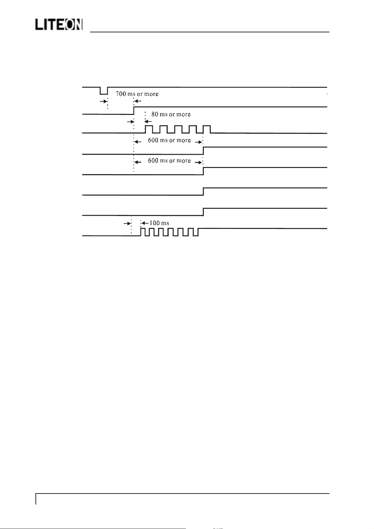
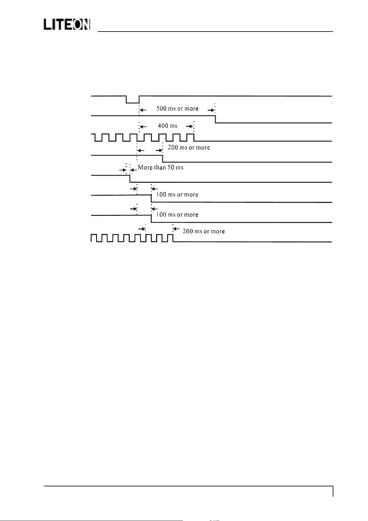
9.6 Power ON sequence
When the POWER switch is pressed, the POWER OFF signal is turned H. When this H potential is detected,
the CPU begins to establish the respective power supplies according to the sequence shown below.
POWER
PPWR
DOTCLK
USBSW
UCPB IAS
LVC C
LED
DATA
Page 6 Circuit Description
Page 9
EC-150ATA
9.7 Power OFF sequence
When the POWER switch is pressed while the power supply is ON, the POWER ON signal is turned H. When
this H potential is detected, the CPU begins to turn off the respective power supplies according to the sequence
shown below.
POWER
PPWR
DOTCLK
USBSW
UCPB IAS
LVC C
LED
DATA
Page 7Circuit Description
Page 10
9.8 List of CPU Pin Assignments
g
)
Port Pin No. Signal Name Initial Setting Function Remark
EC-150ATA
~
P1.0
P1.1
P1.2
P1.3
P1.4
P1.5
P1.6
P1.9
~
P3.0
~
P3.1
P3.2
P3.3
P3.4
P3.5
P3.6
P3.7
~
~
~
~
P2.0
P2.1
P2.2
P2.3
P2.4
P2.5
P2.6
P2.7
~
~
~
~
P0.7
P0.6
P0.5
P0.4
P0.3
P0.2
P0.1
P0.0
~
1
2
3
4
5
6
7
8
9
10
11
12
13
14
15
16
17
18
19
20
21
22
23
24
25
26
27
28
29
30
31
32
33
34
35
36
37
38
39
D4(LEDAMBER
40
41
42
43
44
NC ~ ~
HDATA0 ~ gmZAN1 4bit interface data
HDATA1 ~ gmZAN1 4bit interface data
HDATA2 ~ gmZAN1 4bit interface data
HDATA3 ~ gmZAN1 4bit interface data
HCLK ~
HFS ~ gmZAN1 data enable
VOL_OUT H reserved
PWM ~ Pulse width modulation
RST L Reset CPU Active H
RXD H Receive data
NC ~ ~
TXD H Transmit data
IRQ ~ gmZAN1 interrupt signal
SCL ~ IIC Bus Clock
SDA H IIC Bus Data
DDC-GND L Detect Dsub cable plug-in Active L
P3.6 H External Memory Write Enable
P3.7 H External Memory Read Enable
XTAL2 ~ Crystal signal out
XTAL ~ Crystal signal in
GND ~ ~
NC ~ ~
A8 ~ High-order address byte
A9 ~ High-order address byte
A10 ~ High-order address byte
A11 ~ High-order address byte
A12 ~ High-order address byte
A13 ~ High-order address byte
A14 ~ High-order address byte
A15 ~ High-order address byte
PSEN# H Program store enable
ALE ~ Address latch enable
NC ~ ~
EA# H External Access Enable
D7(USB_ON) H USB HUB power Enable
D6(Uc-PBIAS) H Inverter power Enable
D5(LEDGRN) H LED Green ON
L LED AMBER ON
D3 ~ reserved
D2 ~ reserved
D1(MUTE) L Audio MUTE Enable
D0(AU_SUSP) H Audio SUSP Enable
VCC ~ VCC
mZAN1 4bit interface Clock
Page 8 Circuit Description
Page 11

EC-150ATA
10. Inverter Protective curcuit for back light and power source circuity (Circuit diagram MAIN
PWB 8/10)
This unit operates on an output voltage of 12V from AC adapter. When an AC adapter with an output voltahe
over 12V higher is connected, the control signal from I101 is forcibly connected to the LOW level through D101
(RLZ18B), Q101 (SST33904), and R101, R102. In order to protect the inverter for back light. By this treatment,
oscillation is suspended in the inverter circuit. It must be noted that the back light it unlit as a result of the
stoppage of inverter oscillation.
11. USB circuit
11.1 3.3V cutoff circuit for USB identification (Circuit diagram USB PWB 1/4)
Q905 is a composite transistor where one PNP and one NPN are incorporated in a package.
A signal at pin 1 (5V) of USB (B) connector CN901 passes through R975 (33 ohm) and enters pin 4 (TR2B) of
Q905. Pin 4 is an NPN type base of the internal transistor in Q905. the collector (pin 3) is connected to a 3.3V
circuit through R974 (10 ohm) and R972 (10 ohm) connected in series. The emitter (pin 2) is connected to GND.
For the PNP transistor, on the other hand, a voltage-divided power from the 3.3V circuit is fed to the base (pin 5)
and the collector (pin 1) is connected to UD+ of the USB data line through R901 (1.5 ohm). The emitter (pin 6)
is connected to the 3.3V circuit.
When the USB connector is connected and voltage at pin 1 of CN901 attains 5V, the NPN transistor of Q905 is
turned ON. This also turns on the PNP transistor whose base is connected to the collector of the NPN transistor
through R974 (10 ohm). As a result, the DC+ power supply is fed from the 3.3V circuit that is connected to the
emitter of the PNP transistor, through R901 (1.5 ohm) that is connected to the collector.
When the USB connector is pulled out the host computer is turned off, the base voltage of the NPN transistor at
Q905 is turned to be at the GND level, and therefore the transistor is turned off. As a result, a voltage of 3.3V is
applied to the base of the PNP transistor and this causes the PNP transistor to be turned off also. Finally, a voltage
supply of 3.3V is suspended toward UD+.
IC905 is a step-down type series regulator that generates 3.3V from a 5.2V source.
11.2 USB hub control circuit (Circuit diagram USB PWB 2/4)
IC909 is a reset IC, and IC910 is a USB hub control IC made by NEC.
When the monitor power circuit is turned on, a 3.3V power is fed to IC909. Upon the detection of about 2.75V,
IC909 begins to generate a reset signal of 150msec.
IC910 enables communication with a higher port when UD+ and UD- from the USB connector (Circuit diagram
USB PWB 1/4) are applied to pin 7 and pin 8, respectively. Pin 9, 10, 12, 13, 14, 15, 18 and 19 are connected to
the USB connector (Circuit diagran USB PWB 3/4) of the lower port. They function as a communication interface between lower and higher ports. If an overcurrent is generated in the lower port, it is transferred to the higher
port.
X901 is a crystal oscillator that supplies a 4MHz clock signal to the USB hub control IC (IC910).
11.3 Lower port circuit (Circuit diagram USB PWB 3/4)
CN904 and 905 are the USB lower-port connector.
The 5.2V output from the DC/DC converter passes through the poly-switches of F901, 902, 903 and 904, and is
led to the power supply pins (pin 1 and pin 5 of each connector) of the USB lower-port connector.
An overcurrent signal is given from the poly-switch - USB lower-port connector line to IC910 (Circuit diagram
overcurrent has been generated in the lower port.
11.4 DC/DC converter circuit (Circuit diagram USB PWB 4/4)
IC906 is a DC/DC converter IC, D903 is a rectifier diode, and L910 is a smoothing coil. Pin 5 (ON / OFF) of
IC906 is connected to pin 5 (S/SW) of the USBDC connector CN903 through transistors Q901 and Q902.
When the potential at pin 5 of CN903 is maintained at the GND level, pin 5 of IC906 is aldo at the gnd level and
IC906 stops generation of its output. When pin 5 of CN903 is at the high level, pin 5 of IC906 then stays in the
OPEN state, this causing IC906 to generate a 5.2V output.
Page 9Circuit Description
Page 12

EC-150ATA
Table of Contents
1. No display of screen (Screen is black, color of LED is amber) ----------------------------------------------------- 1
2. Nothing displays on screen (Screen is black, color of LED is green) ---------------------------------------------- 2
3. Checking the back light unit --------------------------------------------------------------------------------------------- 5
4. Abnormal screen ---------------------------------------------------------------------------------------------------------- 6
6. Abnormal Auto adjustment ---------------------------------------------------------------------------------------------- 9
7. Abnormal plug and play operation ------------------------------------------------------------------------------------ 10
7.1 Abnormal DDC1----------------------------------------------------------------------------------------------------- 10
7.2 Abnormal DDC2----------------------------------------------------------------------------------------------------- 10
8. Checking the interface circuit of sync signal -------------------------------------------------------------------------11
8.1 Checking the control circuit of horizontal sync pulse ----------------------------------------------------------11
8.2 Checking the control circuit of vertical sync pulse-------------------------------------------------------------- 11
9. Checking the resolution change IC movement -----------------------------------------------------------------------12
10. No power on -------------------------------------------------------------------------------------------------------------- 13
11. Checking the DC/DC converter circuit --------------------------------------------------------------------------------14
12. Checking the operation of CPU ---------------------------------------------------------------------------------------- 15
13. Checking the audio circuit ---------------------------------------------------------------------------------------------- 16
14. Check the USB hub circuit (NEC Version) ---------------------------------------------------------------------------18
14.1 Hub isnt recognize ------------------------------------------------------------------------------------------------ 18
14.2 Connection apparatus isnt recongnize --------------------------------------------------------------------------19
14.3 Connection apparatus doesnt work -----------------------------------------------------------------------------20
14.4 Check the USB IC ------------------------------------------------------------------------------------------------- 21
14.5 Check the power supply -------------------------------------------------------------------------------------------23
15. Check the USB hub circuit (Atmel Version) -------------------------------------------------------------------------25
15.1 Hub isnt recognize ------------------------------------------------------------------------------------------------ 25
15.2 Connection apparatus isnt recongnize --------------------------------------------------------------------------26
15.3 Connection apparatus doesnt work -----------------------------------------------------------------------------27
15.4 Check the USB IC ------------------------------------------------------------------------------------------------- 28
15.5 Check the power supply -------------------------------------------------------------------------------------------29
Trouble Shooting Index
Page 13

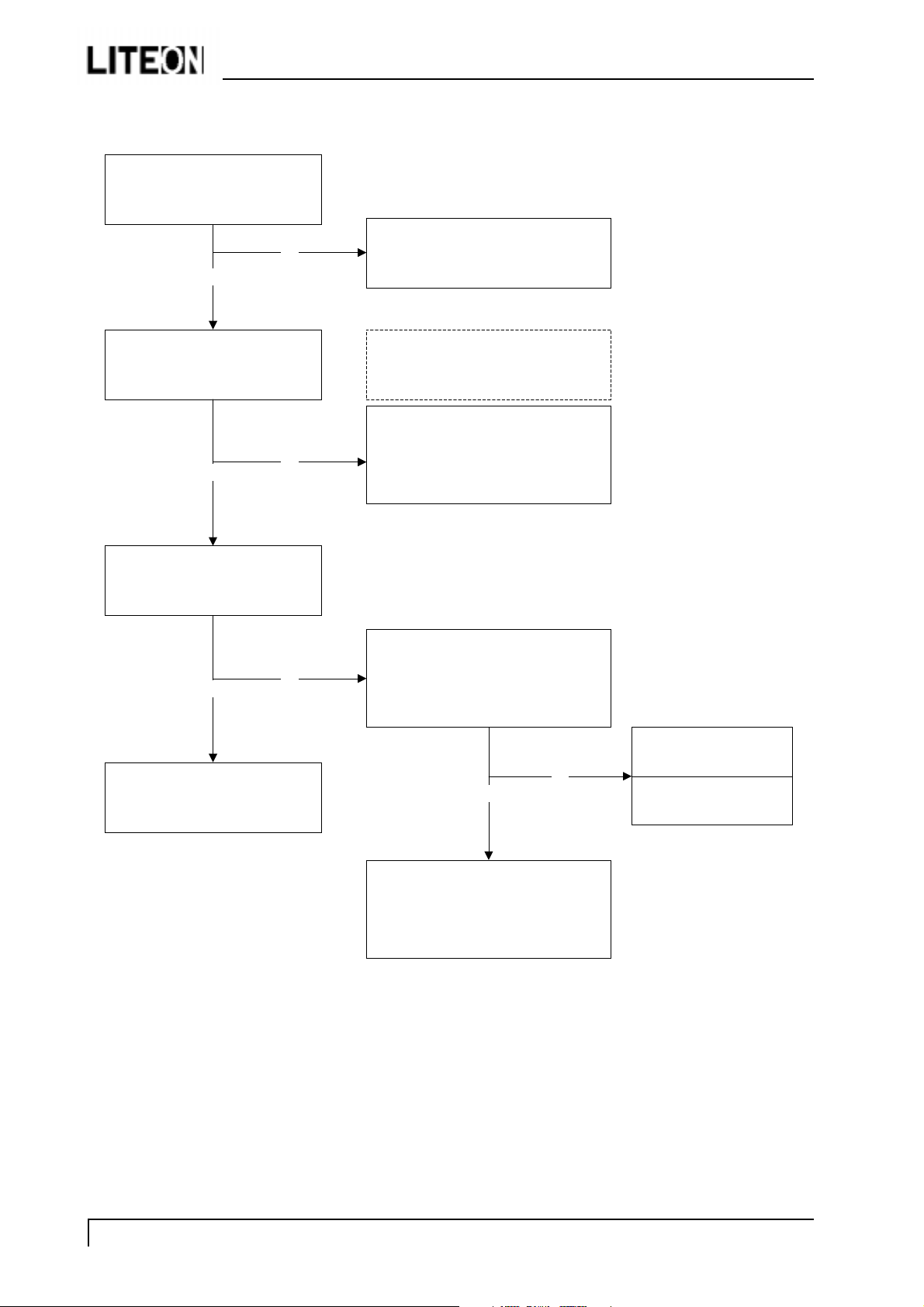
1. No display of screen (Screen is black, color of LED is amber)
Does OSM display when you push
PROCEED button.
Yes
Check if the sync signal from Computer
is output and if the video cable is
connected normally.
No
Preceed "No OSM display"section.
OK
Proceed "Checking the resolution change
IC movement" section.
NG
Input the sync signal of computer, or
change the cable.
When a signal isn't
being inputted, it is
indicated with "VIDEO
INPUT". It is indicated
with "OUT OF RANGE"
at the time of the
frequency that it can't be
distinguished.
EC-150ATA
Trouble Shooting Page 1
Page 14
2. Nothing displays on screen (Screen is black, color of LED is green)
Is backlight lit?
NG Refer "Checking the backlight unit" section
OK
EC-150ATA
Does computer output RGB video signals?
OK
Check OSM menu is displayed on screen
when you push the "PROCEED" key.
OK
Proceed "Abnormal screen" section.
NG
NG
Check the video cable for failure. Check the host for
output signal with all black only.
1) Change pattern of video signal output on the
host.
2) Reconnect the video cable.
3) Change the video cable.
Check if the LCD video signal cable is connected
between the MAIN PWB and LCD module.
NG
OK
Failure Point
The Cable is disconnected.
Next Page
Page 2 Trouble Shooting
Page 15

Continue
Check the 3.3 V power are supplied on I315 pin 2.
Check if the voltage on I315 pin3 that
NG
OK
is high level DC at 5V.
OK
Failure point
NG
EC-150ATA
Failure point
1) Printed wire broke between I314 and I315
2) I314 failure.
I315 Failure
Is a dot clock being outputted under the
condition that a LCD module is connected to
Check the H-sync pulse of negative polarity is
output on P304 pin 38 at TTL level.
Check the V-sync of negative polarity are
P304 pin 44?
OK
OK
output on P304 pin 40.
NG
NG
Failure point
1) I317 failure
2) Printed wire broke between I317 and P304 pin 44.
Failure point
1) I317 failure
2) Printed wire broke between I317 and P304 pin 38.
Failure point
OK
Next Page
NG
1) I317 failure
2) Printed wire broke between I317 and P304 pin 40.
Trouble Shooting Page 3
Page 16

Continue
Check the data enable of positive polarity are output on P304 pin 42.
OK
NG
1) I317 failure.
2) Printed wire broke between I317 and P304 pin 42.
EC-150ATA
Failure point
Check the data signal output on P304 R, G, B
1) The cable broke between P304 and LCD
module.
2) LCD module failure.
data pin.
OK
Failure point
NG
Failure point
1) I317 failure.
2) Printed wire broke between I317 and P304 data line
Page 4 Trouble Shooting
Page 17

3. Checking the back light unit
Is +12V supplied to I316 pin 1 and pin 2, 3.
NG
OK
Is +12V supplied to P306 pin 3, 4 to inverter
Are connected AC adapters normal goods?
PWB?
OK
NG
EC-150ATA
Failure point
An AC adapter is changed to the normal goods.
NG
OK
Check the Uc-PBIAS signal of the rectangle input I313 pin 3 at TTL high level
NG
OK
Check the PWM signal of the input from I302 pin 9 is a PWM signal.
OK
Failure point
Inverter cable disconnection.
Is a "H" level being output in the TTL level from I307 pin 16
Or, is Uc-PBIAS signal of the rectangle being output?
NG
Failure point
Printed wire broke between
I307 pin 16 and I316 pin 3
NG
Failure point
1) Printed wire broke between
I302 pin 9 and I313 pin 5.
2) I104 failure.
Failure point
Printed wire broke between
P307 pin 1 and I316 pin 1, 2 & 3
Failure point
1) Inverter cable disconnection.
2) Inverter of LCD module failure.
Trouble Shooting Page 5
Page 18

4. Abnormal screen
EC-150ATA
Check the R, G, B video signal from computer input on
Check the R, G, B input signals on I317 pin 95, 91, 87,
Is the pulse of the TTL level being output to P304, P305
Check the negative horizontal sync pulse output to P304
D-Sub R, G, B connector.
OK
respectively that their level is 0.7Vp-p maximum.
OK
from the data line of I317?
OK
pin 38 from I317 pin 74 at TTL level.
NG
NG
NG
1) No R, G and B video signal output from host computer. Check
computer
2) Video signal cable disconnection.
In the case of the Red signal. (A Green and Blue signal is the same
path, too.)
1) Printed wire broke between D-Sub(R) and I317 pin 95.
2) R339 short.
3) C330 open.
4) R337 open.
1) Printed wire broke between I317 data line and P305, P304
2) I317 failure.
Failure point
Failure point
Failure point
OK
Check the negative vertical sync pulse output to P304 pin
40 from I317 pin 73 at TTL level.
OK
Check the positive DE pulse output to P304 pin 42 from
I317 pin 43 at TTL level.
OK
Check the SHFCLK OUTPUT to P304 pin 44 from I317
pin 44 at TTL level.
OK
Process "Checking the resolution change IC movement"
section.
NG
NG
NG
NG
1) Printed wire broke between I317 pin 74 and P304 pin 38.
2) R314 open
3) C355 short
1) Printed wire broke between I317 pin 73 and P304 pin 40.
2) R315 open
3) C356 short
1) Printed wire broke between I317 pin 43 and P304 pin 42.
2) R313 open
3) C357 short
1) Printed wire broke between I317 pin 44 and P304 pin 44.
2) FB310 open
3) FB311 open
4) C347 short
5) C378 short
Failure point
Failure point
Failure point
Failure point
Page 6 Trouble Shooting
Page 19

5. NO OSM display
EC-150ATA
Check the output of 5Vp-p pulse from I310 pin 16, 17, 18, 19 when press PROCEED key.
OK
NG
Check the input of IIC signal from I310 pin7 and pin 8.
NG
OK
Check the input of 5Vp-p pulse from I317 pin 118, 119, 120 are same as I310 pin 17, 18, 19, or check
NG
OK
Check the output of IIC Interface from I201 pin 15, 16.
NG
OK
1) Printed wire broke between I310 pin 7 and I201 pin 16.
2) Printed wire broke between I310 pin 8 and I201 pin 15.
input of 5Vp-p pulse from I317 pin 122 is same as I310 pin 16.
1) Printed wire broke between I310 pin 16 and I317 pin 122.
2) Printed wire broke between I310 pin 17 and I317 pin 118.
3) Printed wire broke between I310 pin 18 and I317 pin 119.
4) Printed wire broke between I310 pin 19 and I317 pin 120.
Proceed "Checking the operation of CPU" section.
Failure point
Failure point
ba
Trouble Shooting Page 7
Page 20

ba
Proceed "Checking the resolution change IC movement" section.
Check the +5V is supply on I310 pin 4, 13.
EC-150ATA
NG
OK
Check the input of the dot clock on I310 pin 2 at TTL level.
NG Check the output of the dot clock on I317 pin 117 at TTL level.
OK
Check positive horizontal
sync signal on I310 pin 5
at TTL level.
NG
OK
1) C314 or C315 short.
2) I314 failure
3) Disconnection between I314 pin 2 and I310 pin 4, 13 may have failed.
Proceed "Checking the resolution change IC
NG
OK
1) Printed wire broke between I317 pin 117 and I310 pin 2.
Check the positive horizontal sync signal on I317 pin 115 at TTL level.
Proceed "Checking the resolution change IC
NG
OK
1) Printed wire broke between I317 pin 115 and I310 pin 5.
2) R443 open
Failure point
movement" Section.
Failure point
movement" Section.
Failure point
Check negative vertical sync signal on I310 pin 14 at TTL level.
NG Check negative vertical sync signal on I317 pin 116 at TTL level.
OK
Failure point
I310 failure.
OK
1) Printed wire broke between I317 pin 116 and I310 pin 14.
2) R309 open
Proceed "Checking the resolution change IC
NG
movement" Section.
Failure point
Page 8 Trouble Shooting
Page 21

Check the input of 3.3Vp-p pulse from I317 pin 98,103, 99, 102, 104, 105.
Failure point
NG
1) Printed wire broke between I317 pin 99 and I302 pin2.
OK
2) Printed wire broke between I317 pin 102 and I302 pin3.
3) Printed wire broke between I317 pin 104 and I302 pin4.
4) Printed wire broke between I317 pin 105 and I302 pin5.
5) Printed wire broke between I317 pin 103 and I302 pin6.
6) Printed wire broke between I317 pin 98 and I302 pin7.
Proceed "Checking the resolution change IC movement" section.
EC-150ATA
Trouble Shooting Page 9
Page 22

7. Abnormal plug and play operation
7.1 Abnormal DDC1
Confirm the output of serial data on I311 pin 7 synchronize VCLK at TTL level.
EC-150ATA
1) The host machine isn't communicating in DDC1 mode.
2) The video cable may have failed or may not to have connections for DDC.
3) Between I311 pin 5 and P303 pin 12 may have failed.
4) R336 open.
5) Cable failure.
7.2 Abnormal DDC2
NG
OK
Confirm the output of serial data on I311 pin 6 synchronize SCLK at TTL level.
1) This mode may be in DDC2B
If you change the mode of DDC1, turn off the power switch of the host
and the monitor and power again.
2) I311 failure.
Failure point
Failure point
NG
OK
Failure point
1) The host machine isn't communicating in DDC2 mode.
2) The video cable may have failed or may not to have connections for DDC.
3) Between I311 pin 6 and P303 pin 15 may have failed.
4) R335 open.
5) Cable failure.
Failure point
I311 failure.
Page 10 Trouble Shooting
Page 23

8. Checking the interface circuit of sync signal
8.1 Checking the control circuit of horizontal sync pulse
EC-150ATA
Check the horizontal sync signal on I317
Process "Checking the resolution change IC
pin 150 TTL level.
NG
OK
movement" section.
1) Video cable may have failed.
2) Printed wire broke between P303 pin 13
and I317 pin 150
3) FB306, R350 open
8.2 Checking the control circuit of vertical sync pulse
Failure point
Check the vertical sync signal on I317 pin
Process "Checking the resolution change IC
148 TTL level.
NG
OK
movement" section.
Failure point
1) Video cable may have failed.
2) Printed wire broke between P303 pin 14 and I317 pin
148
3) FB307, R351 open
Trouble Shooting Page 11
Page 24

9. Checking the resolution change IC movement
EC-150ATA
Is there +3.3V supply on I317 pin 77, 79, 84, 96, 92, 88, 8, 129, 136, 139, 137, 143, 11, 21,
NG
OK
Is 50MHz clock input to I317 pin 141
Is +5.0V supplied to I317 pin 100 at
at TTL level?
NG
OK
High level?
NG
OK
Failure point
I317 failure
Print wire broke between X302 pin 5
58, 108, 149, 12, 33, 40 and 65.
Proceed "Checking the DC/DC converter circuit" section.
Is 50MHz clock output from X302
pin 5 at TTL level?
OK NG
and I317 pin 141.
Check the output of 5.0V "H" pulse
from I301 pin 1.
NG Is 5.0V supplied to I301 pin 2?
OK
Is +3.3V supplied to X302 pin 8?
Failure point
OK
NG
OK
Failure point
X302 failure
NG
Print wire broke between and X302
pin 8 and power supply.
Failure point
1) I314 failure
2) L306 open
Failure point
Failure point
Print wire broke between I301 pin 1
and I317 pin 100.
Failure point
I301 failure
Page 12 Trouble Shooting
Page 25

10. No power on
EC-150ATA
Check the +12V power is supplied
from AC adapter.
OK
Is LED turned on in amber
momentarily when a power button is
OK
Check if TTL "H" level is input to
OK
Proceed "Checking the operation of
NG
pushed?
NG
Q305-base.
NG
D323, Q304, R393, R394 circuit
CPU".
Failure point
AC adapter failure.
Failure point
Fuse failure.
Failure point
Trouble Shooting Page 13
Page 26

11. Checking the DC/DC converter circuit
EC-150ATA
Check if the 5V is output from I314
Check the output of 3.3V line voltage
pin 2.
NG
OK
from I315 pin 2.
Check if TTL "H" is output from
Q305-base.
NG Q304, D323, R393, R394 circuit.
OK
Check if the 12V is output from I316
pin 5,6,7,8.
NG I316 failure.
OK
Check the input of 12V to the I314
pin1.
OK
a
Is the output FB321 being inputted
NG
OK
Printed wire broke between I315 pin 2 and IC 317 power supply pin.
OK
to I315 pin 3?
NG
Printed wire broke between I315
Failure point
I315 failure
Failure point
Failure point
pin 3 and output of FB321.
Page 14 Trouble Shooting
Page 27

12. Checking the operation of CPU
Is there +5.0V supply on I302 pin 44
OKNGFailure point
Printed wire broke between output of FB319 and I302 power supply pin.
Is 20MHz clock input to I302 pin 20
and 21 at TTL level?
OKNGFailure point
X301 failure.
Check the input of 5V "H" pulse from
I302 pin 10 are same as I307 pin 1.
(350 msec Typ)
OKNGFailure point
1) Printed wire broke between I302 pin 10 and I307 pin 1.
2) I208 failure.
I302 failure.
EC-150ATA
Trouble Shooting Page 15
Page 28

13. Checking the audio circuit
Is a cable with the host PC
connected?
EC-150ATA
NG
OK
Aren't the setups of the host PC a
minimum and off?
NG
OK
Is correct output waveform being
inputted from JK011 pin 2, 3 of the
OK
Is the waveform which is the same
as JK011 being inputted to I006 pin
OK
Is output wavefrom being outputted
The setup of the host PC is changed.
host PC?
NG
2, 29?
NG
1) Printed wire broke between JK011 pin 2, 3 and I006 pin 2, 29.
2) R047, R048 open.
3) R049, R050 short.
4) C013, C014 open.
in I006 pin 9, 22?
Failure point
Audio cable disconntction.
Failure point
Failure point
Audio cable disconntction.
Failure point
OK
a
NG
Is 9V supplied to I006 pin 10?
NG
OK
Failure point
I006 failure
Is 12V supplied to I008 pin 2?
NG
OK
b
Proceed section 11 "Checking the
DC/DC converter circuit".
Page 16 Trouble Shooting
Page 29

EC-150ATA
a
Is the output waveform which is the
same as I006 pin 9, 22 being
inputted to I007 pin 1,9?
NG
1) Printed wire broke between I006 pin 9, 22 and I007 pin 1, 9.
OK
Is the input waveform amplified by
OK
Is the output waveform of I007 pin
4,6 being inputted to P012 pin 1, 3?
OK
Is the output waveform of P012 pin
1,3 being inputted to p002 pin 1, 3 of
2) C015, C018 open.
3) C015, C018 failure.
4) R051, R052 open.
5) R051, R052 failure.
I007 being outputted?
NG
jack PWB?
Failure point
I007 failure.
NG
Failure point
b
Is the "H" signal of the TTL level
being inputted to I008 pin 1?
Is the "H" signal of the TTL level
NG
being outputted from I208 pin 16?
Proceed section 12 "Checking the
NG
OK
1) C039 short.
2) I008 failure.
Failure point
1) Printed wire broke between I007 pin 4, 6 and P012 pin 1, 3.
2) C016, C017 open.
3) C016, C017 failure.
OK
Printed wire broke between I208 pin
16 and I008 pin 1.
Failure point
operation of CPU".
Failure point
OK
Failure point
1) Disconnection of MAIN PWB and jack PWB.
2) JK001 of Jack PWB failure.
3) Speaker cable disconnection.
4) Speaker failure.
NG
Failure point
Disconnection of MAIN PWB and
Jack PWB.
Trouble Shooting Page 17
Page 30

14. Check the USB hub circuit (NEC Version)
14.1 Hub isn’t recognize
Is a cable with the host PC connected
EC-150ATA
NG
Is a USB cable connected with the monitor?
NG
Is 0.6V supplied to Q905 pin 4?
NG
Is 3.3V supplied to Q905 pin 6?
Failure point
USB cable disconnection
Failure point
USB cable disconnection
Doesn't R975 open
NG
OK
Doesn't R969 open
Failure point
R975 open
NG
Is 3.3V supplied to Q905 pin 1?
NG
Doesn't D909 short with GND?
NG
Proceed "Check the USB IC" section.
proceed "Check the
power supply" section.
Failure point
Q905 failure
Failure point
D909 short
NG
OK
Doesn't Z903 short
NG
OK
Is 5V + 5% supplied to
CN901 pin 1?
NG
OK
Printed wire breaks
between CN901 pin 1
and Q905 pin 4
Failure point
R969 open
Failure point
Z903
Failure point
USB cable failure
Page 18 Trouble Shooting
Page 31

14.2 Connection apparatus isn’t recongnize
Is it aware of the USB hub in the host PC?
EC-150ATA
NG
OK
Is apparatus connected to the down stream port ?
NG
OK
Is 5.2V supplied to CN904 pin1 ,5 ?
NG
Doesn't D904, D905 short with
The un-connection of the down stream port cable.
OK
Doesn't R959, R960, R961
and R962 open ?
NG
OK
Failure point
R959, R960, R961
and R962 open
OK
Is resistance on both ends of
F901, F902 less than 1 Ohm ?
OK
Doesn't D910, D911 short with
GND?
Proceed "Check the power supply" section.
Proceed "HUB isn't recognize" section
Failure point
GND ?
NG
Failure point
D904, D905 short
NG
Failure point
F901, F902 failure.
NG
Failure point
D910, D911 short.
OK
Is 3.3V supplied to IC910
pin 40, 41?
NG
Faulty operation of the over-current protection function.
Failure point
OK
Proceed "Check the USB IC " section.
Trouble Shooting Page 19
Page 32

14.3 Connection apparatus doesn’t work
Is it aware of the USB hub in the host PC ?
EC-150ATA
NG
OK
Is a host PC aware of the peripheral which doesn't work ?
NG
OK
Is the program which is characteristic of the machine
unnecessary to make it work ?
Proceed section 14.1 "HUB isn't recognize".
Proceed section 14.2
"Connection apparatus isn't recognize ".
NG
OK
Is there a precaution of " it doesn't sometimes move via the
hub. " in the manual of the peripheral which doesn't work ?
A machine movement program hasn't been installed.
NG
OK
The HUB un-correspondence of connection peripheral.
Failure point
Failure point
Is the pin of CN904 (pin 2,3 or pin 6,7) with peripheral is
connect with rise_time and fall_time less than 20 nsec ?
NG
In the pin of CN904 (pin 2,3 or pin 6,7 ) which
peripheral is connect with rise_time and fall_time
OK
OK
Proceed section 14.4 "Check the USB IC"
between 100nsec to 300 nsec?
NG
Is the resistance value of R960, R961,
R962 20 Ohm +/-5%?
NG
OK
R959, R960, R961, R962 short.
Failure point
Page 20 Trouble Shooting
Page 33

14.4 Check the USB IC
g
g
g
Is 3.3V supplied to IC910 pin 24, 29,
38 and 39?
NG
OK
Is the reset signal of IC910
pin 6 a Hi
h level (More than 2.3V)?
NG
Does it have the output of the Hi
OK
NG
OK
Is 3.3V supplied to IC909 pin 7?
EC-150ATA
Proceed section 14.5 "Check the power supply ".
h level (More than 2.3V) from IC909 pin 6?
Failure point
Printed wire breaks between
IC909 pin 6 and IC910 pin 6.
Doesn't C917 short with GND?
Failure point
C917 failure
Does it have the output of the Low
level (Less than 0.8V) from IC910
pin 2, 31?
NG
OK
Does it have the output of the Hi
level (More than 2.0V) from IC910
pin 37?
h
NG
OK
Next page
Proceed section
14.5 "Check the
power supply".
Is there an input signal of 1.5V in
OK
NG
OK
Failure point
IC909 short.
Doesn't R949, R950 open?
OK
NG
OK
IC909 pin 2?
NG
Doesn't R916 short?
NG
OK
Is the resistance value if R914
OK
NG
Failure point
IC910 failure
Proceed section 14.5 "Check the power
supply"
Failure point
R916 failure
12k ohm +/- 5%?
Failure point
NG
R914 short
Failure point
R949, R950
open
Trouble Shooting Page 21
Page 34

Continuation
Does X901 oscillate (4MHz)?
EC-150ATA
NG
OK
Isn't IC910 pin 7 fixed on the High
level (More than 2.0V)? And, isn't
IC910 pin 8 fixed on the Low level
(Less than 0.8V)?
NG
OK
Does it have the output of the
High level (More than 2.0V) from
IC910 pin 40, 41?
NG
Does the output of X901 satisfy a Threshold Level
(High: More than 2.3V, Low: Less than 0.8V)?
NG
OK
Failure point
IC910 failure
Failure point
Faulty operation of the host PC.
Failure point
Faulty operation of the over-current protection
Failure point
X901 failure
function.
Failure point
IC910 failure.
Page 22 Trouble Shooting
Page 35

14.5 Check the power supply
Check the 12V power is supplied to CN903 pin 2,6
EC-150ATA
NG
Is the USB DC cable connected ?
NG
Check the 12V
power is supplied
to IC906 pin 1.
NG
Check the 12V
power is supplied
to CN905 pin 5
NG
IC906 pin 5 is not a GND level ?
OK
Failure point
USB DC cable disconnection.
Printed wire breaks between CN903 pin
2,3 and IC906 pin 1.
Failure point
USB DC cable disconnection.
NG
Doesn't C929 open?
Failure point
A USB DC cable isn't
connected .
Failure point
NG
OK
Is Q901 pin 5 a GND level.
NG
OK
Doesn't the resistance value of
R909 short with GND?
Failure point
C929 failure.
Is there Q902-base
more than 0.6V?
NG
Failure point
R941 open
OK
NG
Failure point
R909 failure.
a
OK
Failure point
Q901 failure.
Failure point
Q902 failure.
Trouble Shooting Page 23
Page 36

a
Is 5.2V being outputted from L910 pin 7?
EC-150ATA
NG
OK
Is 5.2V being
outputted from
L911 pin 2?
NG
OK
OK
OK
Is the IC906 output that it had rectification
done by L910 pin 3 being inputted?
NG
OK
Failure Point
L910 failure
Doesn't C911
short with GND?
NG
Doesn't C910
short with GND?
NG
Doesn't C912
short with GND?
NG
Is R913 open?
NG
Failure Point
C911 failure
Failure Point
C910 failure
Failure Point
C912 failure
Failure Point
R913 failure
Doesn't R910 open?
NG
OK
Doesn't D903
open?
NG
OK
Doesn't D903
short with GND?
NG
OK
Isn't output from
IC906 pin 2 fixed
on 12V and the
GND level?
NG
OK
Printed wire
breaks between
IC906 pin 2 and
L910 pin 3.
Failure Point
L913 open
Failure Point
D903 open
Failure Point
D903 failure
Failure Point
IC906 failure
Printed wire
breaks between
L910 pin 7 and
L911 pin 1.
Printed wire
breaks 5.2V.
Page 24 Trouble Shooting
Page 37

15. Check the USB hub circuit (Atmel Version)
15.1 Hub isn’t recognize
Is a cable with the host PC connected
EC-150ATA
NG
Is a USB cable connected with the monitor?
NG
Is a 5V supplied to I201 Pin1?
NG
Is a 3.3V supplied to I201 Pin3?
NG
Failure point
I201
OK
OK
Failure point
USB cable disconnection
Failure point
USB cable disconnection
Doesn't Q203 open
NG
Doesn't R232 open
NG
Failure point
Q203
Failure point
R232 open
Doesn't 3.3V to J202 pin2
OK
NG
Doesn't R201 open
NG
Failure point
R201
OK
OK
Printed wire breaks
between R201 and J202
" Proceed section 15.4 Check the USB IC "
OK
OK
Doesn't R235 open
NG
Doesn't Q204 open
NG
Doesn't R233 open
NG
Doesn't I203 open
NG
Proceed section 15.5
"Check the power supply"
Failure point
R235
Failure point
Q204
Failure point
R233 open
Failure point
I203
Trouble Shooting Page 25
Page 38

15.2 Connection apparatus isn’t recongnize
Is it aware of the USB hub in the host PC?
EC-150ATA
NG
OK
Is apparatus connected to the down stream port ?
NG
OK
Is 5V +/- 5% supplied to J204 pin1 ,5 ?
NG
OK
Doesn't L209, L211 open ?
NG
OK
Failure point
L209, L211 open.
OK
The un-connection of the down stream port cable.
Doesn't C215, C216, C217,
C218 short with GND ?
Is resistance on both ends of
R225, R206 less than 1 Ohm ?
OK
Is 5V supplied to IC201 pin 9 ?
Proceed section 15.5 " Check the power supply "
Proceed section 15.1 "HUB isn't recognize"
Failure point
NG
C215,C216,C217,C218 short
NG
Failure point
Failure point
R225, R206 failure.
NG
Faulty operation of the over-current protection function .
Failure point
OK
Proceed section 15.4 " Check the USB IC ".
Page 26 Trouble Shooting
Page 39

15.3 Connection apparatus doesn’t work
Is it aware of the USB hub in the host PC ?
EC-150ATA
NG
OK
Is a host PC aware of the peripheral which doesn't work ?
NG
OK
Is the program which is characteristic of the machine
unnecessary to make it work ?
Proceed section 15.1 "HUB isn't recognize".
Proceed section 15.2
" Connection apparatus isn't recognize ".
NG
OK
Is there a precaution of " it doesn't sometimes move via the
hub. " in the manual of the peripheral which doesn't work ?
NG
A machine movement program hasn't been installed.
The HUB urn-correspondence of connection
OK
Failure point
Failure point
peripheral.
Is the pin of J204 (pin 2,3 or pin 6,7) with peripheral is connect
with rise_time and fall_time less than 20 nsec ?
NG
In the pin of J204 (pin 2,3 or pin 6,7 ) which peripheral
is connect with rise_time and fall_time between
100nsec to 300 nsec?
NG
OK
OK
Proceed section 15.4 "Check the USB IC"
Is the resistance value of
R213,R214,R215,R216 22 Ohm +/-5%?
OK
NG
R213,R214,R215,R216 open
Failure point
Trouble Shooting Page 27
Page 40

15.4 Check the USB IC
Is 5V supplied to I201 pin 1 ?
NG
Does it have the output of the
High level (More than 4.75V )
from I201 pin 9,10,12
EC-150ATA
Proceed section 15.5 " Check the power supply ".
NG
Proceed section 15.5 " Check the power supply ".
Does X201 oscillate (6 MHz) ?
NG
Isn't I201 pin 15 fixed on the
High level ( more than 2.0V ) ?
and isn't pin14 fixed on the
Low level ( less than 0.8v ) ?
NG
Faulty operation of the host PC.
Does it have the output of the High Level
( more than 4.75V ) from I201 Pin 9.
NG
Does R234 open ?
Does the output of X201 satisfy a threshold level
( High:more than 4.75V,Low:less than 0.8V) ?
OK
Failure point
I201 failure
Failure point
NG
Failure point
X901 failure
NG
OK
Does Q205 short ?
NG
OK
Does Q201 short ?
NG
OK
Failure point
Faulty operation of the over current protection function.
Failure point
I201 failure
Failure point
R234 failure
Failure point
Q205 failure
Failure point
Q201 failure
Page 28 Trouble Shooting
Page 41

15.5 Check the power supply
Check the 12V power is supplied to J201 pin 2,6
EC-150ATA
NG
Is the USB DC cable connected ?
OK
NG
Check the 12V
power is supplied
to I202 pin 1.
NG
OK
USB DC cable disconnection.
Printed wire breaks between J201 pin 2,6
OK
Check the 5V
power is supplied
to J201 pin 5
NG
USB DC cable disconnection.
OK
I202 pin 5 is not a GND level ?
NG
Is Q202 collector a GND level
OK
Is the 5V being output
from L201 pin 2 ?
OK
Failure point
I202 failure
Failure point
Failure point
and I202 pin 1.
Failure point
NG
A USB DC cable isn't connected .
Doesn't Q202 open
NG
OK
Failure point
Q202 failure
Failure point
Failure point
Printed wire breaks between Q202 pin 1
and I202 pin 5.
NG
OK
Is the 5V being
output from L214
pin 2 ?
NG
Doesn't C209,C220,C222
short with GND ?
OK
OK
Printed wire breaks 5V
Printed wire breaks
between L201 pin 2 and
Is the I202 output that it had
rectification done by L201 pin
1 being inputted?
NG
OK
Failure point
L201 failure
NG
L214 Pin 1 .
Failure point
C209, C220, C222
Doesn't D205 open?
NG
OK
Doesn't D205 short
with GND?
NG
OK
Isn't output from I202
pin 2 fixed on 12V and
the GND level?
NG
OK
Printed wire breaks
between I202 pin 2
and L201 pin 1.
Failure point
D205 open.
Failure point
D205 failure.
Failure point
I202 failure.
Trouble Shooting Page 29
Page 42

EC-150ATA
1. Recommended Parts List
Note: 1. The components identified by mark are critical for X-ray safety. Replace these with
only the same parts specified.
2. There is only OTP IC at the model beginning (FPR stage or before). When it put in mass
production and there must be Mask coming out. If you have spart parts need, please use BOM
to get the last release part number and related information.
No. Location Part Number Description
1 INVA 6716008900 INVERTER DC-AC 12V DA00812600L
2 PWR 6716006704 ADAPTER A-D 12V/4A GRAY GL5B
3 V002 6712450070 FFC 45P 0.5 2896 (ATYPE) 73/223
4 V003 6712300060 FFC 30P 0.5 2896 (ATYPE) 35/253
5 D318 6412001738 DIODE RLS4148 LL-34 SMD ROHM
6 D319 6414056038 DIODE ZNR RLZ TE-11 5.6B LL-34
7 D321 6413045008 DIODE SCHOTTKY BYS10-45-TR SMD
8 D323 6414180048 DIODE ZNR RLZ TE-11 18B LL-34
9 F301 6851105092 FUSE SLOW TR5-T CG90L=4.3+-0.3
10 I301 6444006810 IC MCP130-450DI TO92 MICROCHIP
11 I302 6448015548 IC P87C51RD+IA 44P PLCC PHILIPS
12 I303 6446002506 IC 74HCT04 14P SMD
13 I305 6448016128 IC 24LC16B/P 8P DIP MICROCHIP
14 I307 6446006018 IC 74HCT373 20P 300mil SOP PHI
15 I308 6446002406 IC 74HCT08 14P SMD
16 I310 6444007408 IC MTV130P-30 16P SOP MYSON
17 I311 6448007420 IC AT24C21-10PC-2.5 8P PDIP
18 I312 6442027408 IC Si9424DY 8P SOP
19 I313 6442001908 IC LM358DT 8P SOP ST
20 I314 6442024106 IC LM2596S-5.0 5P TO263(S) NS
21 I315 6442023316 IC RC1587M33 3P TO263 SMD
22 I316 6442027308 IC Si4431DY 8P SOP
23 I317 6444007308 IC gmZAN1 160P PQFP GENESIS
24 L307 6111307130 COIL CHOKE 3uH K DRWW6x8 G3
Recommended Spare Parts List Page 1
Page 43

No. Location Part Number Description
25 P304 6610450010 PLUG 45P 0.5 IL-FHR-45S-HF JAE
26 P305 6610300030 PLUG 30P 0.5 IL-FHR-30S-HF JAE
27 Q301 Q302 6422003508 TR NPN PMBT2222A SOT-23 PHILIPS
28 Q305 6422007308 TR NPN SST3904 T116 SOT-23 SMD
29 D600 6418004401 LED LTL-36EDIP 1(Y)3(G) LITEON
30 S601 6853004413 SW TACT TSAD-1 1KEY BLACK 4PIN
EC-150ATA
Page 2 Recommended Spare Parts List
Page 44

LITE-ON TECHNOLOGY CORP.
5 F, No. 16, Sec. 4, Nanking E. Road, Taipei, Taiwan
Tel: 886-2-25706999 Fax: 886-2-25706888
URL:// www.liteontc.com.tw
Printed in Taiwan
 Loading...