

Page 1

Service Manual
19-inch Color Monitor
C1996NSL/NST/PNST
Page 2
Service Manual Versions and Revision
No. Version Release Date Revision
1. 1.0 Dec. 5, 2001 Original release
Copyright
Copyright 2001 LiteOn Technology Corp.
All Rights Reserved
This manual may not, in whole or in part, be
copied, photocopied, reproduced, translated, or
converted to any electronic or machine readable
form without prior written permission of LiteOn
Technology Corp.
C1996NSL/NST/PNST Service Manual.
Printed in Taiwan.
Trademarks
LiteOn is a registered trademark of LiteOn
Technology Corp.
All other trademarks are the property of their
respective owners.
Page 3
C1996NSL/NST/PNST
Table of Contents
1. Precautions.........................................................................................................2
2. Product Specifications .......................................................................................5
3 Control Location and Functions ...................................................................... 10
4. Operation Theory.............................................................................................. 11
5. Alignments and Adjustments ........................................................................... 16
6. Troubleshooting............................................................................................... 21
7. Recommended Spare Parts List ....................................................................... 27
8. Block Diagram ................................................................................................ 29
9. Exploded Diagrams ..................................................................................Inserted
10. PCB Diagrams ......................................................................................... Inserted
11. Schematic Diagrams ................................................................................ Inserted
Page 1
Page 4
C1996NSL/NST/PNST
1 Precautions
Follow these safety and servicing precautions to prevent damage and to protect against potential hazards
such as electrical shock and X-rays.
1-1 Safety Precautions
1-1-1 Warnings
1. For safety purpose, do not attempt to modify
the circuit board, and always disconnect the AC
power before performing servicing on the
monitor.
2. Operation of the monitor outside its cabinet or
with the cover removed involves the risk of
shock hazard. Repair work on the monitor
should only be attempted by service personnel
who are thoroughly familiar with all necessary
safety precautions and procedures for working
on high voltage equipment.
3. Do not lift the CRT by the neck. After
completely discharging the high voltage anode,
handle the CRT only when wearing shatterproof
goggles. Try to keep the CRT away from the
body during handling.
4. High voltage should always be kept at the rated
value, no higher. Only when high voltage is
excessive are X-rays capable of penetrating the
shell of the CRT. Operation at high voltages
may also cause failure of the CRT or high
voltage circuitry.
nonmetallic control knobs, insulating materials,
cabinet backs, adjustment and compartment
covers or shields, isolation resistor-capacitor
networks, mechanical insulators, etc.
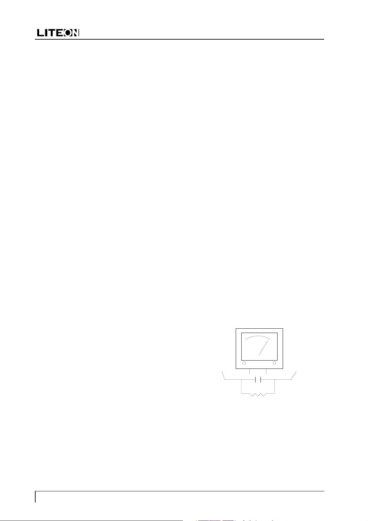
3. AC Leakage Current Check
Always perform the AC Leakage Current
Check on the exposed metal parts, including
metal cabinets, screwheads and control shafts,
as follows:
a) Plug the AC line cord directly into a rated
AC outlet. Do not use an isolation
transformer during the check.
b) Use an AC voltmeter with at least 5000
ohms per volt sensitivity as follows:
Connect a 1500 ohms, 10 watt resistor
paralleled by a 0.15uF AC capacitor in series
with all exposed metal cabinet parts and a
known earth ground, such as electrical
conduct or electrical ground connected to
earth ground, as shown in the Figure 1-1.
Measure the AC voltage across the
combination of resistor and capacitor.
Figure 1-1. Set Up For AC Leakage Current Check
5. The CRT is especially constructed to limit Xray emission to 0.5mR/HR at 300 microamperes
anode current. To ensure continued X-ray
protection, replace the CRT with only the same
or equivalent type as the original, and adjust the
anodes voltage to the designated maximum
rating, never to exceed.
1-1-2 Safety Checks
Before returning the monitor to the user, perform
the following safety checks:
1. Inspect to make certain that each lead dress is
not pinched or that hardware is not lodged
between the chassis and other metal parts in
the monitor.
2. Inspect all protective devices such as
Page 2
To kno w n
earth ground
0.15ufd
1500 ohm 10 watt
To exposed m e tal
cabinet part
c) Reverse the AC plug at the AC outlet and
repeat the steps for AC voltage
measurements for each exposed metal part.
d) Voltage reading must not exceed 0.3 volts
RMS, equivalent to 0.2 milliampere AC. Any
value exceeding this limit ill constitute a
potential shock hazard and must be
corrected immediately.
Page 5
C1996NSL/NST/PNST
1-1-3 Product Safety Notices
Many electrical and mechanical parts in this chassis have special safety-related characteristics which are
often not evident from visual inspection, the protection afforded by them may not be obtained by replacing
them with components rated for higher voltage, wattage, etc. Before replacing any of these components,
consult the Recommended Spare Parts List given at the end of this manual. Any of the replacements that do
not provide the same safety characteristics may result in shock, fire, X-ray emission or other hazards.
1-2 Servicing Precautions
Warning: An electrolytic capacitor installed with the wrong polarity might explode.
Caution: Before performing servicing covered by this service manual, read and follow the Safety Precautions
section of this manual.
Note: If unforeseen conflict between the following servicing precautions and any of the safety
precautions, always follow the safety precautions
1. Follow closely the servicing precautions printed on the monitor cabinet and chassis.
2. Always unplug the AC power cord from the AC power source before removing or installing any component
or assembly, disconnecting PCB plugs or connectors and connecting a test component in parallel with a
capacitor.
3. When replacing parts or circuit boards, clamp the lead wires around the component before soldering.
4. When replacing a high wattage resistor (>0.5W metal oxide film resistor) in the circuit board, keep the
resistor about 1 cm (1/2 inch) away from the circuit board.
5. Keep wires away from the high voltage or high temperature components.
6. Keep wires in their original positions so as to minimize interference.
7. Always connect a test instruments ground lead to the instrument chassis ground before connecting the
positive lead; always remove the instruments ground lead last.
After putting the rear cover back and make sure the monitor is working properly, the Hi-Pot &
Ground Continuity tests MUST BE performed before the monitor is returned to user.
1-3 Hi-Pot Test
1. Test Equipment
Puncture test model PM5530 ADT or KIKUSU TOS-8750 voltage tester or equivalent approved equipment.
Note : The test equipment must be calibrated in regular period.
2. Test Setup
a) Apply voltage : DC 2100 VDC
b) Test duration : 3 seconds
c) Cutoff current should be set to 3 mA
3. Test Procedure
a) Unplug power cord from AC source.
b) Put the power switch of the monitor in the ON position.
c) Leave signal cable un-connected.
Page 3
Page 6
d) Plug monitor power cord to the Hi Pot tester terminals.
e) Turn on tester and watch the indicator or beeper.
f) If the indicator lamp lighten, or beeper beeps, the test fails.
1-4 Ground Continuity Test
1. Test Equipment
AC low ohm tester TOS-6100 or equivalent approved equipment.
Note :The test equipment must be calibrated in regular period.
2. Test Setup
a) Test duration : 3 seconds
b) Set current limit at 25 A
c) The grounding resistance must be less than 0.1 ohm.
3. Test Procedure
a) Plug the monitor power cord to the tester terminals.
C1996NSL/NST/PNST
b) Make sure all connections are well-contacted.
c) Turn on monitor power and tester power.
d) Press Test button.
e) If green light shows up, means test OK.
If red light shows up, means test fails.
f) If the Tester has a digital display, the resistance value must not exceed 0.1 ohm.
Note :Be sure not to touch the metal portion of the signal cable head during testing.
Page 4
Page 7
C1996NSL/NST/PNST
2 Product Specifications
2-1 Specifications
19-inch, (18-inch visual image area) sloted mask, 90 degrees
Picture Tube
Scanning Frequency VGA, Super VGA, 1024x768@75/85 Hz, 1280x1024@85 Hz
Maximum Resolution 1600 dots (H) x 1200 lines (V) @75Hz refresh rate
Display Area 350 mm (H) x 262 mm (V) typical
Display Characters 80 char. x 60 rows on a 10 x 10 matrix
deflection, dot type black matrix, medium short persistence
phosphor, dark tint, non-glare/ anti-static screen,
0.26 mm dot pitch
Display Colors Analog
Input
Synchronizatin Signals Separate Sync: horizontal/vertical, TTL, positive or negative
Synchronization
Frequencies
Signal Connectors 15-pin, D-shell connector
Video Signals Analog : 0.7 Vp-p, RGB positive
Power Input 120 Watts (maximum) AC rated voltage, 100VAC to 240VAC
Misconvergence Center Area : <
User Controls
Service Controls PWB-1596/1598 : power voltage adjust (VR801)
Preset Modes 10 (see Table 2-2. Timing Chart)
Unlimited Color s
Horizontal : 30 to 96 kHz
Vertical : 50 to 160 Hz
0.3 mm; Corner Area : < 0.4mm
Power On/O ff, C ontrast, Brightness, Horizontal Size,
Horizontal Position, Vertical Size, Vertical Position,
Pincushion, Trapezoid, Pin Balance, Parallelogram, Rotation,
Color temperature, Language, Display Frequency, Degauss,
Recall, H. Moire, V. Moire
focus 1 , focus 2
Environmental
Considerations
Operation temperature : 5
Operation Humidity : 20% to 80% ambient
Storage temperature : -40
Storage Humidity : 5% to 95% (non-condensing)
Altitude : up to3000m above sea level
o
C to 35oC ambient
o
C to 65oC ambient
Note: Above specifications are subject to change without prior notice.
Page 5
Page 8
2-2 Signal Cable Pin Connections
Table 2-1. Signal Cable Pin Assignment
Pin Signal Pin Signal
1Red video 9 +5V
2 Green video 10 Digital Ground
3 Blue video 11 Ground
4 Ground 12 SDA
5* Ground 13 H- Sync
6 Red ground 14 V- Sync/VC L
7 Green ground 15 SCL
8 Blue ground
C1996NSL/NST/PNST
Note: * This pin is used for selftest detection. Connect this pin to ground at the PC end.
Page 6
Page 9

C1996NSL/NST/PNST
2-3 Timing Chart
This section describes the timings that the computer industry recognizes as standard for computer-generated
video signals.
Table 2-2. Timing Chart
Mode 12345678910
H. Dots 640 720 640 832 800 1152 1024 1600 1280 1600
V. D o t s 480 400 480 624 600 870 768 1200 1024 1200
H-fre q (kHz) 31.47 37.927 43.27 49.725 53.67 68.681 68.67 75 91.146 93.75
Sync Polarity -- - - + -+ -++
A pe riod us
B Bla nking us 6.356 6.085 5.33 5.586 4.409 3.04 3.725 3.457 2.844 2.765
C Sync us 3.81 2.028 1.556 1.117 1.138 1.28 1.016 1.185 1.016 0.948
D B.P. us 1.907 3.042 2.22 3.91 2.702 1.44 2.201 1.877 1.422 1.501
E Active us 25.42 20.282 17.78 14.524 14.222 11.52 10.836 9.877 8.127 7.901
F F. P. us 0.636 1.014 1.556 0.559 0.569 0.32 0.508 0.395 0.406 0.316
V-freq (Hz) 59.94 85 85 74.55 85 75.062 84.99 60 85 75
Sync Polarity -+ - - + - + - ++
G Period ms 16.68 11.759 11.76 13.414 11.756 13.322 11.765 16.667 11.761 13.333
H Blanking ms 1.43 1.213 0.67 0.864 0.578 0.656 0.582 0.667 0.527 0.533
I Sync ms
J B.P. us 1.02 1.107 0.578 0.764 0.503 0.568 0.524 0.613 0.483 0.491
K Active us 15.25 10.546 11.09 12.549 11.179 12.667 11.183 16 11.235 12.8
L F.P. us 0.35 0.026 0.023 0.04 0.019 0.044 0.015 0.013 0.011 0.011
31.78 26.366 23.11 20.11 18.631 14.561 14.561 13.333 10.971 10.667
0.064 0.079 0.069 0.06 0.056 0.044 0.044 0.04 0.033 0.032
Seperate Sync
Horizontal
C
E
Vid eo
D
Sync
A
B
F
H.Parameters:
A: Period B: Blanking Time
C: Sync Width D: Back Porch
E: Active Time F: Front Porch
Ve r ti c a l
I
K
Vid eo
J
Sync
G
H
L
V.Parameters:
G: Period H: Blanking Time
I: Sync Width J: Back Porch
K: Active Time L: Front Porch
Page 7
Page 10
C1996NSL/NST/PNST
2-4 Power Saving Function
Note: The monitor will be driven into Power Saving mode by the control signal from the display
controller, as indicated by the amber-color power LED.
Table 2-3. Power Saving Function
LE
State Power
Consumption
ON <120 watts Green
D
Light
Active
OFF
The power saving states will be kept until a control signal has been detected or the keyboard or mouse is activated.
The recovery time from Active OFF state back to ON state is around 10 seconds.
<3 watts Amber
2-5 TCO Version (Optional)
The monitor meets the TCO 99, NUTEK energy saving, electric and magnetic field requirements.
2-5-1 TCO 99 Version (Optional)
The emission from magnetic and electric field must comply with the limits specified by the Swedish Board
for Measurement and Testing, commonly known as MPR 1990 recommendations. These limits are
summarized in the Table 2-4.
Table 2-4. TCO 99 Requirements
Page 8
OCT/FLVOCT/FLE
dleiFcitengaMTn52Tn002
dleiFcirtcelEm/V1m/V01
egnaRycneuqerFzHk004~2zH0002~5
eulaVSMRSMR
ecnatsiDmc03mc03
citatsortcelE
laitnetoP
V005-/+V005-/+
Page 11
C1996NSL/NST/PNST
The monitor is designed with selected CRT and carefully routed wires around CRT, make sure exactly the
same routing scheme is used when doing CRT replacement.
The TCO 99 scheme is for international and environmental labelling of personal computers. The labelling
scheme was developed as a joint effort by the TCO (The Swedish Confederation of Professional Employ
ees), Naturskyddsforeningen (The Swedish Society for Nature Conservation) and NUTEK (The National
Board for Industry and Technical Development in Sweden).
1)`Scope
TCO 99 touches on ergonomic qualities, emissions (electrical and magnetic fields), energy efficiency and
ecology (with demands for environmental adaptation for both the product and the production processes at
the manufacturing plant).
2) Environmental Requirements
The monitor abides by the environmental demands concerning restrictions on the presence and use of
heavy metals, brominated and chlorinated flame retardants, CFCs (freons), and chlorinated solvents,
among other things. The monitor is also recyclable.
3) Energy Requirements
The monitor also follows the energy requirements that, after a certain period of inactivity, the monitor
shall reduce its power consumption to a lower level in one or more stages.
4) Others
The monitor meets the strict environmental demands for the reduction of electric and magnetic fields,
physical and visual ergonomics and good usability.
Table 2-5. TCO 99 Visual Ergonomics
erutaeFdradnatSnoitpircseD
ytiraeniLsselro%1 ehtotderapmocsworrosnmulocfohtgnelniecnereffiD
.rotinomehtforetnecehthguorhtshtgnelgnidnopserroc
ecnanimuLyalpsiD)tsaelta(2m/dc001
ecnanimuL
ytimrofinU
erutarepmetroloC
noitairav
morfsnoitcelceR
gnisac
£G 'v'u¡Ø 10.0
¡Ù /%02¡Ø ssalg03.elbat&tenibacnosinoitarnoitcelferehT
sselro1:5.1 ehtnihtiwecnanimulnimotxamehtneewtebsioitarehT
.aeraevitcaelohw
Page 9
Page 12
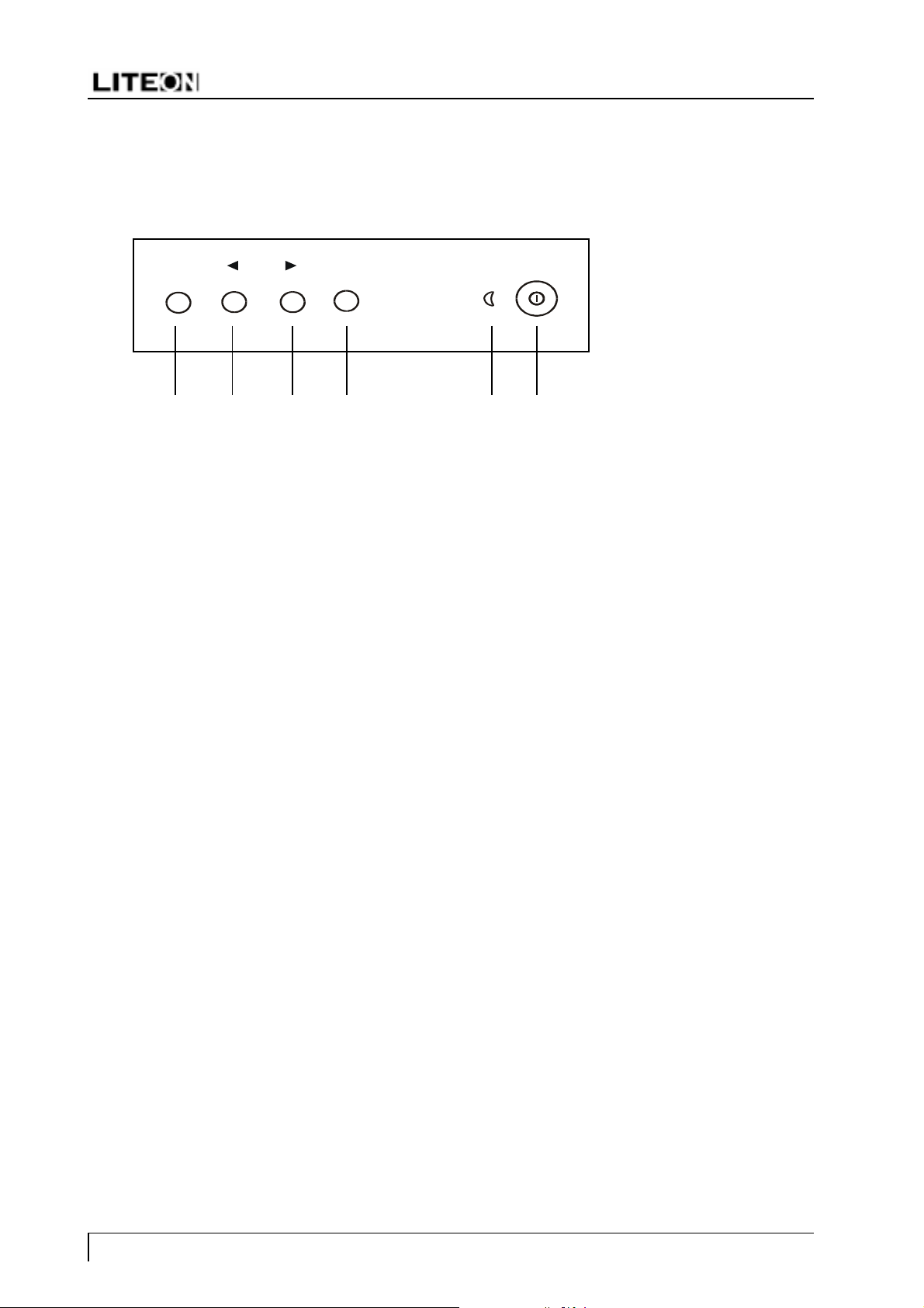
3 Control Location and Functions
C1996NSL/NST/PNST
12
(1) (2)
(3) (4)
(5) (6)
(1) Function Key
(2) Decrease Key
(3) Increase Key
(4) Select Key
(5) Power LED
(6) Power ON/OFF
3-1 Front Panel
3-2 Front Panel Keys Functions
1. Function Key: Display the main menu, and exit the adjustment screen and save adjustments.
2. Decrease Key: Scroll across main menu, highlighting control to be adjusted. Decrease value of selected
control. Toggle between Contrast and Brightness adjustment screens.
3. Increase Key: Scroll across main menu, highlighting control to be adjusted. Increase value of selected
control. Toggle between Contrast and Brightness adjustment screens.
4. Select Key: Press once to display adjustment screen. Press again, for some controls, to toggle between
controls shown in pairs on main menu.
5. Power LED: Display different modes (ON, OFF) of the monitor by showing different color for each
mode.
6. Power ON/OFF: To turn the monitor ON and OFF.
3-3 Adjustment Procedure
1. Press (6) key to turn on the monitor.
2. At normal condition, press (1)on the front panel to activate the on-screen manager (OSM) menu.
3. To select a user control, press (2) or (3) key repeatedly until the control is highlighted.
4. To adjust the value for a particular control, press (4), then press the (2) or (3) key to obtain the desired
value. There are a few parameters that do not require any adjustment, like Manual Degauss, Memory
Recall.
5. Some controls are grouped in pairs on the main menu. Press (4) key to toggle between them.
6. To save your adjustments and exit screen, press (1) key. The menu will automatically clear out from the
screen if no keys are pressed within 30 seconds.
Note: To enter the Internal Adjustment mode, press (1) & (4) keys simultaneously then press (6).
Page 10
Page 13

C1996NSL/NST/PNST
4 Operation Theory
This is a fully digital controlled multi-sync color monitor that is compliant with DDC1/2B Plug and Play
VESA standard and offers the following main features.
4-1 Main Features
1. Simplified design with minimum components.
2. The NOVATEK NT68P65AU processor-- that has I
brightness-- offers the functions for: (a) Contrast, (b) Brightness, (c) H-size, (d) H-position, (e) V-size, (f)
V-position, (g) Pincushion, and (h) Trapezoid, (i) Pin Balance, (j) Parallelogram.
2
C bus controlled geometric correction, contrast and
In addition, it also offers more functions as: (a) Sync. processor, I/P and O/P, (b) Mute, (c) Power saving
off, (d) Power saving override, (e) DDC2B, (f) I
2
C Bus for auto-alignment through signal cable (g) CS
switching for linearity and size compensation, (h) High voleage adjustment, (i) G2 voltage adjustment.
3. Stores up to 10 factory preset modes and offers 6 user modes. There are 18 function icons in OSD. They
are controlled by
2 keys on the front panel.
1
4. Powerful PHILIPS TDA4841 and TDA4863 present the following useful functions: (a) Pincushion, (b)
Trapezoid, (c) V-Position, (d) V-Size, (e) Verticals C and S correction -- factory adjust, (f) Pincushions
V. position correction, (g) Corner correction -- factory adjust, (h) Pincushion unbalance correction -factory adjust, (i) Parallelogram distortion -- factory adjust, (j) Moire cancellation, (k) X-ray protection,
and (l) Full horizontal and vertical auto sync capability.
5. Software controlled auto shut off function activated if fH < = 29 kHz and fH > = 96 kHz.
6. Full range AC input and simplified line filter design.
4-2 Microcontrol Section
1. This monitor uses NOVATEK NT68P65AU CPU. It contains a 8-bit CPU core, 256 bytes of RAM used
as working RAM and stack area, 24k bytes of OTP ROM, 14-channel 8 bit PWM D/A converter, 2channel A/D converters for key detection saving I/O pins, internal H. sync and V. sync signals processor
providing mode detection, and an I2C bus interface. When H/V sync through D-Sub signal cable enter pin
41 and pin 42, the CPU performs frequency / polarity detection and calculate and send to H/V sync OUT.
Then CPU reads the data from I703 and transfer to device 4841 and some DAC in CPU, above operation
takes about 500 ms.
2. There allows 10 factory preset modes and 6 user modes. There are 8 functions, Contrast, Brightness, H.
Size, H. Position, V. Size, V. Position, Pincushion, and Trapezoid, all controlled by OSD icon which can
be adjusted by user.
3. The pin 25 and pin 26 are used for ATE function. When CPU receives C6 as slave address, it will operate
in ATE mode which is used for auto-alignment. After alignment the data will be stored in I703.
4. The user control parameters are selected by OSD icons, through
2 keys, they are detected by
1
sensing the voltage through R710, R759, R713, R714, R709, R711, R760 to pin 16 and 17 of I701.
4-3 Deflection Section
1. I2C -- autosync deflection controller is TDA4841.
2. The TDA4841 is a high performance and efficient solution for autosync monitors. All functions are
controllable by I
control all functions.
2
C bus. SDA and SCL signals coming from microprocessor feed to pin 19 and pin 18 to
Page 11
Page 14

C1996NSL/NST/PNST
4-3-1 Horizontal Section
1. The oscillator is driven by the currents in R472 and R468. The minimum oscillator frequency is determined
by R472 and the maximum frequency is determined by R468.
2. Horizontal sync goes into pin 15 through R494. And horizontal flyback pulse goes into pin 1 through R479
and bypass filter C445 from Emitter of Q407 and C412, C433, C411, R419, C456, R421, D413 for AFC
loop.
3. Horizontal driver (pin8) output to Q401 via C401, Q401 switching to drive T401 provide IB1/IB2 current
then turn on/off Q402 and switching the yoke current.
4-3-2 Vertical Section
1. Vertical sync goes into pin 14 through R493.
2. The free running frequency is determined by R470 and C442.
4-3-3 Vertical O/P section
1. The differential output currents from pin 13 of Vout1 and pin 12 of Vout2 can be directly coupled to the
vertical deflection booster pin 3 and pin 2 of TDA4863.
2. The TDA4863 has two output stages which are current driven in opposite phase and operate in combination
with the deflection coil in a half bridge configuration.
3. This IC is powered by three sets of positive voltage. (+13V at pin1, 37V at pin 8, -13V at pin 6)
4-3-4 E-W/Trapezoid and H. Width Controls
1. The scan current is determined by B+ (the voltage of C413) that is obtained from step down circuit
output. Step down circuit include Q404, T402, D407.
2. I401 TDA4841 pin 6 (B DRV) will drive the step down circuit to change H. width.
3. EW DRV (pin11) provides a complete EW drive waveform including parabola, corner and trapezoid
correction and feed to BIN (pin 5 of I401) to get a good control for pincushion / trapezoid / corner.
4. The top and bottom corner correction can be adjusted seperately.
4-3-5 X-Ray Protection
1. To avoid X-ray hazard, a DC voltage generated at pin 6 of FBT and rectified by D107, C111 and divided
by R476, R477 and R478 come into pin 2 of TDA4841.
2. If this voltage is higher than 6.39 V, then TDA4841 will be activated to float HUNLOCK (pin17), H.
DRV( pin 8), B DRV (pin 6), VOUT1 (pin 12), VOUT2 (pin13). After that all deflection circuit stop
working.
4-3-6 Blanking and Brightness
1. The vertical blanking signal comes from I401 pin 16 and vertical sync. These two pulses combine into
Q542 and Q541. This signal feets into T501 pin 24.
2. In protection mode or out of range or mode change mute signal will turn high and turn on Q107.
G2 voltage will drop from 600V to 250V.
3. The brightness is control by I
2
C bus. The output pins are I501 pin 14, pin 15, pin16.
Page 12
Page 15

C1996NSL/NST/PNST
4-3-7 Contrast Section
1. Contrast is controlled by I701 through I2C bus to I501 (LM1267) directly.
2. Beam current is detected through T101 (FBT) pin 7, D106, C109, Q102, R108, R121, R122 to control
I501 pin 22 voltage. When I501 pin 22 voltage drops below 5V, the ABL function will happen.
4-3-8 Dynamic focus circuitry
The dynamic focus is applied to improve the corner focus performance, it includes horizontal and vertical
dynamic focus.
1. Vertical dynamic comes from I401 pin 32 and is amplified through C105, Q101, C137, and feed to FBT
dynamic focus pins R133, R132, Q101.
2. This amplifier need 200V voltage supply, it comes from FBT pin 8 and rectified through L102, D101, and
C102.
4-4 Power Supply Section
4-4-1 AC Rectifier
The circuit can accept 90 V to 264 V AC input through D801 bridge diodes and C808 filtering to get DC 126
V~364 V for power conversion in T802.
4-4-2 Line Filter
It consists of C801, C802, C803, C816, C820, C823, T801, T804 and meets EMI regulation.
4-4-3 Power LED Status
1. The LED has 3 leads with common cathode to emit green and amber color light for different power
saving states.
2. Normal : Green light
3. Off Mode : Amber light
4-4-4 Auto Degaussing
When S801 turns on, pin 27 of I701 will send a signal to Q802 and turns on RL801 for degaussing. After 4
seconds, it will turn off RL801 automatically.
4-4-5 PWM Control
1. Start Up
The I801 (KC3843B) gets power from R846, Q821, R849, R848, D826, D828, D822 and pin 7 voltage
reaches 8 V for starting up. The I801 starts oscillation at 22 kHz, sawtooth on pin 4 and pin 6 output to
drive Q803/T802. Once Q803 switching on, D806, C804 set up an 15 V to keep I801 working through
D821 auxiliary voltage.
2. Regulation
The DC O/P voltage is proportional to the auxiliary voltage, so I801 pin 2 senses the feedback voltage
from the divider R802, R823, VR801 and R820 to compare with the built-in 2.5 volts reference voltage for
error amplifier operation. Finally pin 6 can modulate the different duty cycle by VR801 setting to achieve
regulation purpose.
Page 13
Page 16

C1996NSL/NST/PNST
4-4-6 Synchronization
1. Normal Mode
The sync pulse from FBT (31 kHz~95 kHz) via R812, R831, C815, R826, D824, C814 and R816 to pin 4
of I801 to keep I801 synchronized with horizontal sync input frequency.
2. Power Saving Modes: Off mode
Because there is no pulse from FBT, so the free-run frequency is decided by R817 and C814 and the
SMPS works at 22 kHz.
3. Override
The horizontal free run frequency is about 62.5 kHz under override condition, SMPS is synchronized to
this frequency.
4-4-7 O.V.P.
If the auxiliary voltage is higher than zener voltage ZD807 (20 volts) and makes pin 3 of I801 higher than
1 V, pin 6 duty cycle is limited to have the OVP activated.
4-4-8 O.P.P.
The excess current of T802 through R813, R814, R834, C813, R865 and R864 can develop enough voltage
on pin 3 then limit the power delivered because the pin 6 duty cycle is limited too.
4-4-9 High Voltage Generation with F.B.T.
1. The H. V generation circuit combines T101 F.B.T. with I101 TL494/KA7500 PWM control circuit.
2. When I101, Vcc(pin12) reaches at 12V, pin 5,6 gets a freerun sawtooth waveform about 25KHz, and
approximately 5.7Vp-p, when voltahe at pin 15 is higher than pin 16 (5V reference) then release pin 3 to
be controlled by pin 1 feedback signal and compare with pin 5 to output PWM.
3. HFLB1 is used to trigger pin 5 via Q112, to synchronize the deflection circuit.
4. PWM output will drive Q116 & T101 to gererate high voltage (26KV), T101 pin 11, 15 becomes DC/AC
feedback, with the voltage link to I101 non-inverting input pin 1 to stabilize H.V (26KV) and VR101 can
be adjusted to control H.V value.
5. When X.R.P occur, the hunlock will keep high to pull down I101 pin 2 and shut down PWM output.
4-5 Video Amplifier Section
1. RGB signal inputs are terminated by R501, R531 and R561 then pass through the coupling capacitors
C501, C531 and C561 to IC501 LM1267 preamplifier.
2. The amplifier RGB signals (0~4 Vpp) are adjusted by I
comes from pin 16 of TDA4841.
3. The video output stages are amplified by I901(LM2465). The RGB cathodes cut off are adjusted by I
bus control by internal icon.
2
C bus from I501, pin 23 is for clamp pulse which
2
C
4. Under override condition, CHECK SIGNAL will show up on the screen.
4-6 OSD (On Screen Display) Circuit
Page 14
Page 17

C1996NSL/NST/PNST
1. The I502 NT6827-00002 is OSD IC. The OSD signals are worked by positive vertical pulse from I701 pin
32 that goes through R554 to I502 pin 10, and positive horizontal pulse from HFLB1 through R527 to I502
pin 5. CPU I701 pin 27, 28 (I2C bus) transfers information to I502 pin 7, 8.
2. The OSD R. G. B signals and blanking signal are terminated at I502 pin 15, 14, 13, and 12 feed into I501
pin 1,2,3, and 4, then the OSD picture appears.
Page 15
Page 18

C1996NSL/NST/PNST
5 Alignments and Adjustments
This section of the service manual explains how to make permanent adjustments to the monitor settings.
5-1 General Adjustments
5-1-1 Adjustment Conditions
a) Power Supply
Apply AC 115 V or 220 V
b) Warm-up Time
The monitor must be powered on for 15 minutes before starting any alignment, but requires 30 minutes of
warm-up time for convergence adjustment.
c) Signal Input
1. Video: RGB Analog, 0.7 Vp-p, positive
2. Synchronization: Horizontal and vertical TTL signal, separate, positive or negative
3. All adjustments should be made using a signal of FH = 91 kHz, FV = 85 Hz, unless otherwise defined.
5-1-2 Equipment Required
The following equipments are necessary for adjustment procedures:
1. Volt-ohm-A meter (Sanwa FD-750C or equivalent)
2. 30 kV high voltage probe (HP34111A)
3. Oscilloscope (TEK2235 or equivalent)
4. Minolta Color Analyzer II
5. Signal generator (COMPAQ PC with proper display cards or Chroma 2250//2225)
6. Screwdriver
5-1-3 Switching Power Supply and Regulator Adjustment
a. The regulated B+ control has been preset in the factory and needs no adjustment. However, if any repair
is made on the power supply section, the following readjustment procedures are recommended:
1. Allow the monitor to warm-up for about 15 minutes.
2. Apply XGA (1280 x 1024 @ 91 kHz/85 Hz) signal to the monitor.
3. Connect a DC voltage meter to TP001 end, and adjust VR801 for 10.7
4. If a fuse is broken during adjustment, remember to replace it with the exact same type of fuse.
+ 0.1 V DC
b. If necessary, follow the following procedures to enter the factory mode.
1. Press both
2. After turn the power off, monitor will go back to normal mode.
key and 2 key simultaneously then power On.
1
Page 16
Page 19

5-2 Alignment Procedures
5-2-1 High Voltage Adjustment
CONDITION
Display image : Crosshatch pattern
5-2-2 Screen and White Balance Adjustment
CONDITION
C1996NSL/NST/PNST
Press
and 2 buttons simultaneously when switching the power On.
1
Display image : No video
PROCEDURE
1 Raster color setting
1-a Adjust HV icon to set high voltage = 26KV.
1-b Adjust G2 icon to set G2 at 600 ± 5V
1-c Set Brightness icon maximum to 40%
1-d Select OSD icon to R.G.B. cutoff
1-e Set G gun cutoff to 0.5 ± 0.15 FL
1-f Adjust R/B cutoff to get x=283 ± 5, y=297 ± 5, Y=0.6 ± 0.2 FL
1-g Set Brightness to cutoff , get Y=0.01 ~ 0.03 FL
1-h Set Brightness to minimum.
CONDITION
Display image : 50 mm x 50 mm white block pattern
PROCEDURE
2 6500
0
K color temperature setting
2-a Set Brightness to cutoff and Contrast to 75 Value
2-b Move cursor on OSD to choose color temperature icon.
2-c Press
key to G gain then adjust G gain = 70 value, then adjust B, R to x=313±5, y=329±5.
2
2-d Check x=313±5, y=329±5.
3 9300
0
K color temperature setting
3-a Move cursor on OSD to choose color temperature icon.
3-b. Press
key to G gain then adjust G gain = 75 value, then adjust B, R to x=283±5, y=297±5.
2
3-c Adjust Contrast max. to set Y=38±2FL
3-d Check x=283±5, y=297±5.
3-e Adjust Contrast min. to set Y=1.0FL.
4 Full white ABL setting
Page 17
Page 20

C1996NSL/NST/PNST
CONDITION
Display image : full white pattern
4-a Set Brightness to cutoff and Contrast to maximum.
4-b Move cursor to choose ABL inside contrast icon.
4-c Adjust ABL to set Y=32±1FL
4-d Repeat all the procedures in 5-2-2 section until the best white balance is obtained.
5-2-3 Focus Adjustment
CONDITION
Display image : e character pattern
PROCEDURE
1. Set Brightness to cutoff and Contrast to maximum.
2. Adjust top VR at T101 (static focus VR) to make vertical line clear.
3. Adjust center VR at T101 (dynamic focus VR) to make horizontal line clear.
4. Repeat above procedures to get best focus.
5-2-4 Dynamic focus Adjustments
1. Horizontal dynamic focus set Hf=370V ±10 V in phase (compare with Vcp signal).
2. Vertical dynamic focus set Vf=145V ±10V in phase.
5-2-5 Static Convergence Adjustments
Static convergence involves alignment of the red, blue and green lines in the center area of the display.
Note : The monitor requires 30 minutes warm-up time for convergence adjustment.
CONDITION
Page 18
Page 21

Display image : Crosshatch pattern
Warm-up Time : 30 minutes
PROCEDURE
1. Set Brightness and Contrast to display a well-defined pattern.
2. Ensure the convergence magnet rings are correctly positioned on the CRT.
Figure 4-1. Convergence Magnets on the CRT
1
11
+
C1996NSL/NST/PNST
P
CRT
FRONT
8 7 6 5 4 3 2
10
1) Setup Bolt 2) Bow Magnet 3) Band
5) Spacer 7) Spacer
9) Holder
6) 6-Pole Magnet
9
4) 4-Pole Magnet
8) 2-Pole Magnet
11) Tabs10) Band
3. Rotate the individual rings of 4-pole convergence magnets by changing the spacing between the 2 tabs to
converge the vertical red and blue lines at the center of the screen.
4. Rotate the pair of rings of 4-pole convergence magnets by maintaining spacing between the 2 tabs to
converge the horizontal red and blue lines at the center of the screen.
5. Rotate the individual rings of 6-pole convergence magnets by changing the spacing between the 2 tabs to
converge the vertical red, blue and green lines.
6. Rotate the pair of rings of 6-pole convergence magnets by maintaining spacing between the 2 tabs to
converge the horizontal red, blue and green lines.
7. Repeat the steps from 3~6 until the best convergence is obtained.
Figure 4-2. 4-pole and 6-pole Magnets Movement
Red/
Bl u e Gre en
6-pole magnets
movem e nt
Blue
Red
Bl u e Red
Red/
Blue
Green
4-pole magnets
movem e nt
Note : The 4-pole magnets and the 6-pole magnets interact, making dot movement complex.
Page 19
Page 22

C1996NSL/NST/PNST
5-2-6 Degaussing
Degaussing is required when poor color impurity appears on the screen. This monitor uses an automatic
degaussing circuit that is activated when the power is on. The automatic degaussing will be fully functional
again after the monitor has been in operation for 20 minutes.
The degaussing effect is confined to the picture tube since the coils are mounted at the back of the tube.
Should any part of the chassis or cabinet becomes magnetized, it is necessary to degauss the affected area
with a manual degaussing coil.
5-2-7 Manual Degaussing
1. Apply line voltage to the degaussing coil and move it in a rotary motion over the front, sides, and top of the
monitor. The coil should be kept away from the rear of the monitor to avoid damaging the magnetic neck
components.
2. Slowly rotate and move the coil away from the monitor to about 6 feet beyond the point where no effect
on the CRT will be noticeable.
For proper degaussing, it is essential that the field be gradually reduced by moving the coil slowly away from
the monitor. The degaussing coil must never be shut off or disconnected while near the monitor, as this would
introduce a strong field instead of canceling the effect of the stray fields.
Page 20
Page 23

6 Troubleshooting
6-1 No Raster
C1996NSL/NST/PNST
No Raster
Measure
voltage of B+ at
T402 pin 2 on
PWB-MAIN
0 V
Short Circuit
at load?
Yes
Check DC B+ line,
Q402, Q404
No
Check I801,
Q803, R814,
R813, ZD807,
ZD801, R811,
R861, D825
cathode, heater, Grid
Check
AC I/P on
C808
Yes
Normal
(137 V, 91kHz)
Check voltage of
1, Grid 2, etc.
No
D801,T801,
R804, T804,
High
(175 V or more)
Check I401
Check
F801
Page 21
Page 24

6-2 OSD Abnormal
C1996NSL/NST/PNST
OSD Abnormal
Check I502
missing?
No
Check R516,
R526, R527
OK?
Yes
Check J516,
R556 OK?
Yes
Yes
No
No
Put on
I502
Replace them
Replace it
Page 22
Replace I502
Page 25

6-3 Function Key Abnormal
Function Key Abnormal
C1996NSL/NST/PNST
Check I701 and
I703 missing?
No
Power
ON/OFF again and
check X701, oscillator
OK?
Yes
Check
I703 EEPROM content
OK?
Yes
Yes
No
No
Put on
I701, I703
Replace X701
Replace I703 or do
ATE again
Replace I701 and check
uP OK?
No
Check
pin 5 of I701
is 5V?
No
Replace I705
Yes
Yes
Replace I701
Check
R732, C713
Page 23
Page 26

6-4 No Vertical Scan (Raster is one horizontal line)
No Vertical Scan
Check
I301 voltage of
pin 1 is 12V, pin
2 is 37V and
pin 4 is
-14V?
Yes
No
C1996NSL/NST/PNST
Check or replace
I301.
Check
pin 5 O/P waveform
at I301
Normal
Check
pin 6, 7 of I301
waveform
Still no vertical scan
Check or replace CRT
Abnormal
Replace I301
Page 24
Page 27

6-5 Out of Horizontal Synchronization
Out of Horizontal
Synchronization
C1996NSL/NST/PNST
Horizontal
sync present at
pin 15 of I401
Yes
Check
I401 pin 8 H output
frequency
Yes
Check Q401, T401,
Q402, R402, R403,
C404, R404, D402, Q410
6-6 Out of Vertical Synchronization
Out of Vertical
Synchronization
No
No
Ckeck or replace
the signal cable or
I701
Check or replace
the signal cable
or I701
Vertical sync
present at
pin 14 of I401
Yes
Check
I401 pin 24 ramp
frequency
Check C442
No
Ckeck signal cable &
vertical sync input &
I701
Page 25
Page 28

6-7 R.G.B. Video Amplifier Abnormal
RGB Video AMP Abnormal
C1996NSL/NST/PNST
Check
waveform at I501 pin 18, 19
and 20
Yes
Check
I901 pin 1, 3 and 2 voltage
and wave form
Yes
Video signal present at the
pin of the CRT R.G.B.
Cathode
Yes
Check or replace the
No
signal cable or I501
No
Replace I901
Defective cut-off circuit
(DC restore)
6-8 Blank EEPROM Trouble-shooting:
Description of functions for models under C1996 series EEPROM DATA AUTO-RELOAD
The function allows plant staff to pre-write and customer service personnel to use blank EEPROM
through the pre-write EEPROM function whenever the CPU is implemented. The method of operation
is as follows:
First, press the HOT KEY, start after C1996 turns to (<&>) KEY. At this point of time, the CPU
is capable of detecting the first 8 DATA of each page that EEPROM contains. When the
reading goes to 00H or FFH, the EEPROM PAGE will turn to blank; instead, the pre-set value
is being written into the EEPROM through CPU. Otherwise, it shall be deemed an effective
value and that the pre-write function shall not be activated.
Page 26
Page 29

C1996NSL/NST/PNST
7 Recommended Parts List
Note:1. The components identified by mark are critical for X-ray safety. Replace these with
exactly the same parts specified.
2 . There is only OTP IC at the model beginning (FPR stage or before). When it put in mass
production and there must be Mask coming out. Please check BOM to get the last release part
number and related information.
No. Location Part Number Description
1 C407 6325943252-03 P=22.5 PPS 4300P 1800V
2 C808 6312633126 ALU uF 330 400V F 85C 25x40
3 D801 6417001000 TS4B05G-01
4
5
6
7
8
9
10
11
12 I802 6442014000 IC LTV-817D
13 T404 6139000500 XFRMER H-CENT THC1005 5mH
14
15
D814 D815
D402
D407
D817 D119
D831 D813 6412002937 DIODE FUF 5407AMP 3A/800V
**
F801 6851504053 / 51 FUSE TIME LAG 5ST4 4A/250V
**
I301 6442026400 IC TDA4863 9P (PHILIPS)
***
I401 6442030000 IC TDA4841 32P SDIP (PHILIPS)
**
I501 6442031500 IC LM1267
**
I701 6448017800 IC NT68P65AU 42P PDIP NOVATEK(FLASH)
**
Q402 6421004310 TR NPN 2SC5411 (TOSHIBA)
***
Q404 6427000900 FET P-CHNL SFS9634
***
6412020007 DIODE SF34 3A/200V
6412014707 PUP5406
16
17 Q115 6426006400 FET N-CHNL IRFS630A SAMSUNG
18
19 R803 6203459017 POSISTOR 4.5 OHM Q 2PINPITCH=10
20 R804 6201100062 THERMISTOR 10 OHM 5A P=7.5 TKS
21
22 T401 6135003400 XFRMR HOR DRIVE THD-1034 EI19
Q116 6426005410 FET N-CHNL IRFS840A
***
Q803 6426009600 FET N-CHNL 2SK2996 TOSHIBA
***
R818 6422002925 FS OHM 0.27 1W J HOR
***
Page 27
Page 30

C1996NSL/NST/PNST
No.
23 T101 6133093010 FBT TFB-9301 FM159R-B
24 T402 6111444130 COIL CHOKE 4.4MH
25 T801 6138002201 LINE FILTER TLF-1016A 16mHET28
26 T802 6131052500/510 XFRMER PWR TPW-1087 EE40
27 X701 6449006900 CRYSTAL 12MHz TOP8.000 30pF TOP
28 ** I901 6442032300 LM2465 9P
29 I402 6442005900 LM324 14P
30 *** I801 6442006720 KA3843B
31 I301 6442026400 IC TDA4863 9P (PHILIPS)
32 R813 6221215852 0.15 OHM 2W
33 ** I703 6448015720 MICRO CHIP IC 24LC08B-8P
34 D818 6412019907 SF24
Location Part Number Description
35
36 C413 632627456-03 MPP 0.27U 250V TAI PMS
37 C421 6326210453-03 MPP 0.1u 250v TAI PMS
38 C423 6326322443 MPP 0.22u 250V HJC
39 C425 6326262442 MPP 0.62u 250V HJC
40 C427 6326215542 MPP 1.5u 250V HJC
41 V901 6811192608 M46QCE261X112 SAMSUNG
Q406 Q410
Q403
6421003800 KSD882
Page 28
Page 31

8 Block Diagram
B
R
G
ABL
I502
NT6827
OSD
5V
HFLB1
VTTL
CLBL
SCL1
SDA1
HFLB1
V
Blanking
Q541
Q542
P501
B-IN
R-IN
G-IN
LM1267
VIDEO PREAMP
R
G
B
CLBL
RGB
LM2465
RGB
CUT OFF
ADJUST
Q901
Q902
Q931
Q932
Q961
Q962
Q903
Q933
Q963
HEATER
C1996NSL/NST/PNST
R
G
B
G1 G2
FOCUS 2
HV
FOCUS 1
P502
P702
SCL
SDA
DDC 5V
LED
CLBL
HFLB
SDA 1
SCL 1
O/R
SCL
SDA
V SYNC
H SYNC
KEY
CONTROL
VTTL
HFLB1
6.3V
G2 CONTROL
I701
NT6861 AU
VIDEO 5V
GENERATOR
VTTL
HTTL
SCL1
SDA1
OFF
CLBL
GND
10.7V
80V
I401
TDA 4841
10.7V
10.7V
180V
D. FOCUS
VOUT 1
VOUT 2
XRP
P505
I101
PWM CONTROL
TL494/KA7500
HFLB1
H DRIVER
Q402
D403
C407
B+
DRIVER
Q404
T402
180V
Q116
FBT
DRIVER
Q115
CANCELING
CKT
80V
LINEARITY
CONTROL
T403
H CENTER
Q403
VR401
T101
FBT
T102
+H
-H
+V
-V
200V
48V
G2
G2 CONTROL
CONTROL
CKT Q105
Horizontal
Dynamic focus
DY
XRP
CKT
C137
R132
ABL
P301
V
DYNAMIC
P801
D701
4.3V
D703
SCL1
SDA1
5V
I705
13V
L
N
FG
LINE
FILTER
Q807
BRIDGE
DIODE
E2PROM
LOW VOLTAGE
DROP DOWN
I703
2404
DEG
CKT
I801
SMPS
VERTICAL
O/P
I301
TDA4863
-14V
POWER
O/P
T802
-14V
80V
180V
10.7V
13V
13V
7V
37V
10.7V
SWITCH
Q813
10.7V
Page 29
Page 32

Page 33

Page 34

Page 35

Page 36

Page 37

LITE-ON TECHNOLOGY CORP.
5 F, No. 16, Sec. 4, Nanking E. Road, Taipei, Taiwan
Tel: 886-2-25706999Fax: 886-2-25706888
URL:// www.liteontc.com
Printed in Taiwan
 Loading...