

Page 1

Service Manual
17-inch Color Monitor
A1770NSL/NST
Page 2
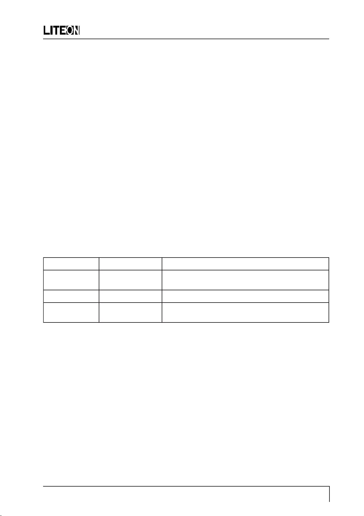
Service Manual Versions and Revision
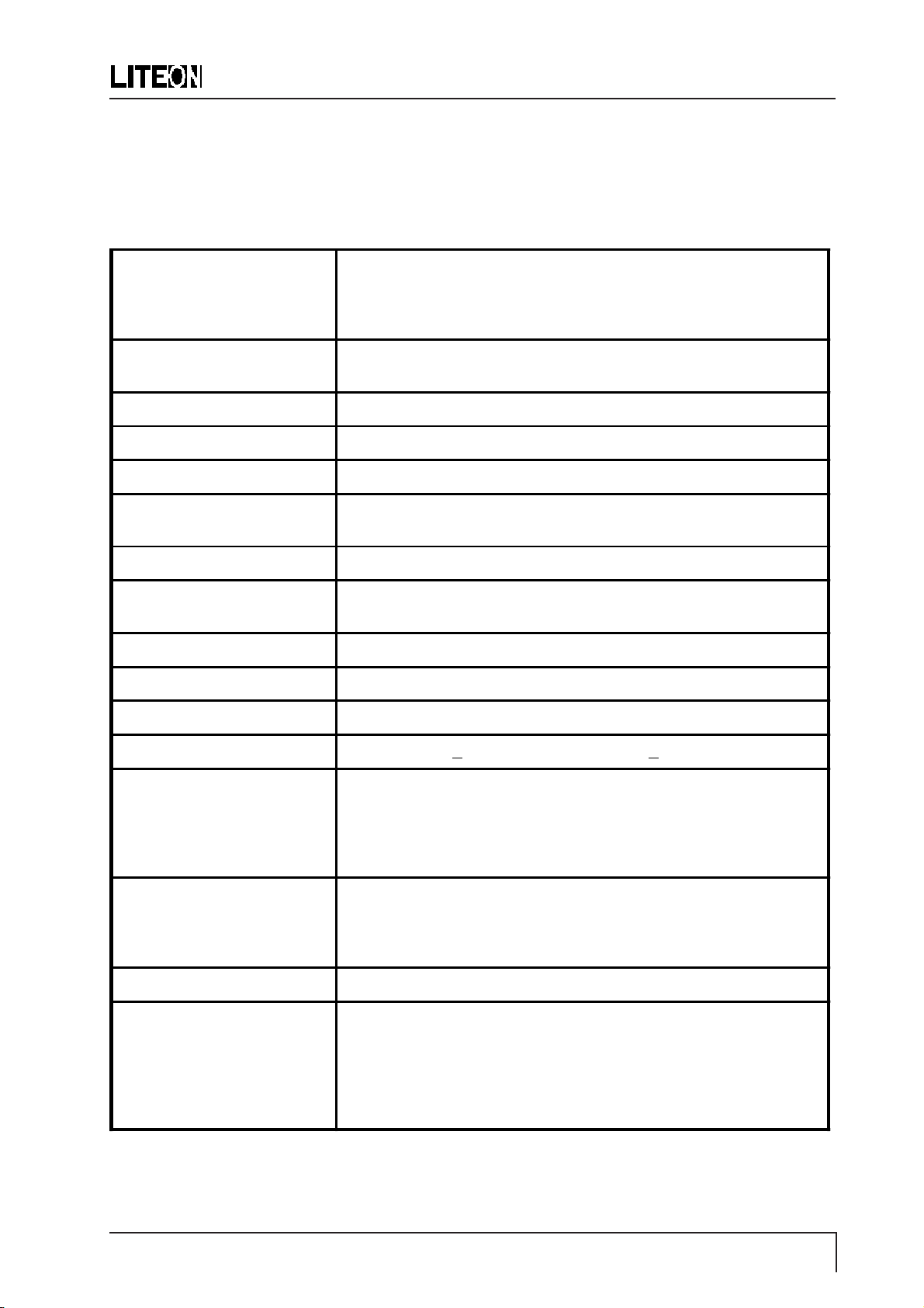
No. Version Rele ase Date Revision
1. 1.0 July 17, 1998 Original release
Copyright
Copyright 1998 LiteOn Technology Corp.
All Rights Reserved
This manual may not, in whole or in part, be
copied, photocopied, reproduced, translated, or
converted to any electronic or machine readable
form without prior written permission of LiteOn
T echnology Corp.
A1770NSL/NST Service Manual.
Printed in Taiwan.
T rademarks
LiteOn is a registered trademark of LiteOn
Technology Corp.
All other trademarks are the property of their
respective owners.
Page 3

A1770NSL/NST
Table of Contents
1. Precautions.........................................................................................................2
2. Product Specifications .......................................................................................5
3 Control Location and Functions ...................................................................... 10
4. Operation Theory..............................................................................................11
5. Alignments and Adjustments ........................................................................... 16
6. Troubleshooting............................................................................................... 21
7. Recommended Spare Parts List....................................................................... 27
8. Block Diagram ................................................................................................ 29
9. Exploded Diagrams.................................................................................. Inserted
10. PCB Diagrams......................................................................................... Inserted
11. Schematic Diagrams ................................................................................ Inserted
Page 1
Page 4
A1770NSL/NST
g
1 Precautions
Follow these safety and servicing precautions to prevent damage and to protect against potential hazards
such as electrical shock and X-rays.
1-1 Safety Precautions
1-1-1 Warnings
1. For safety purpose, do not attempt to modify
the circuit board, and always disconnect the AC
power before performing servicing on the
monitor.
2. Operation of the monitor outside its cabinet or
with the cover removed involves the risk of
shock hazard. Repair work on the monitor
should only be attempted by service personnel
who are thoroughly familiar with all necessary
safety precautions and procedures for working
on high voltage equipment.
3. Do not lift the CRT by the neck. After
completely discharging the high voltage anode,
handle the CRT only when wearing shatterproof
goggles. Try to keep the CRT away from the
body during handling.
4. High voltage should always be kept at the rated
value, no higher. Only when high voltage is
excessive are X-rays capable of penetrating the
shell of the CRT. Operation at high voltages
may also cause failure of the CRT or high
voltage circuitry.
nonmetallic control knobs, insulating materials,
cabinet backs, adjustment and compartment
covers or shields, isolation resistor-capacitor
networks, mechanical insulators, etc.
3. AC Leakage Current Check
Always perform the AC Leakage Current
Check on the exposed metal parts, including
metal cabinets, screwheads and control shafts,
as follows:
a) Plug the AC line cord directly into a rated
AC outlet. Do not use an isolation
transformer during the check.
b) Use an AC voltmeter with at least 5000
ohms per volt sensitivity as follows:
Connect a 1500 ohms, 10 watt resistor
paralleled by a 0.15uF AC capacitor in series
with all exposed metal cabinet parts and a
known earth ground, such as electrical
conduct or electrical ground connected to
earth ground, as shown in the Figure 1-1.
Measure the AC voltage across the
combination of resistor and capacitor.
Figure 1-1. Set Up For AC Leakage Current Check
5. The CRT is especially constructed to limit Xray emission to 0.5mR/HR at 300 microamperes
anode current. To ensure continued X-ray
protection, replace the CRT with only the same
or equivalent type as the original, and adjust the
anode’s voltage to the designated maximum
rating, never to exceed.
1-1-2 Safety Checks
Before returning the monitor to the user, perform
the following safety checks:
1. Inspect to make certain that each lead dress is
not pinched or that hardware is not lodged
between the chassis and other metal parts in
the monitor.
2. Inspect all protective devices such as
To kn own
earth
round
0.15ufd
1500 ohm 10 w att
To ex posed m e tal
cabinet part
c) Reverse the AC plug at the AC outlet and
repeat the steps for AC voltage
measurements for each exposed metal part.
d) Voltage reading must not exceed 0.3 volts
RMS, equivalent to 0.2 milliampere AC. Any
value exceeding this limit ill constitute a
potential shock hazard and must be
corrected immediately.
PrecautionsPage 2
Page 5
A1770NSL/NST
1-1-3 Product Safety Notices
Many electrical and mechanical parts in this chassis have special safety-related characteristics which are
often not evident from visual inspection, the protection afforded by them may not be obtained by replacing
them with components rated for higher voltage, wattage, etc. Before replacing any of these components,
consult the Recommended Spare Parts List given at the end of this manual. Any of the replacements that do
not provide the same safety characteristics may result in shock, fire, X-ray emission or other hazards.
1-2 Servicing Precautions
Warning: An electrolytic capacitor installed with the wrong polarity might explode.
Caution: Before performing servicing covered by this service manual, read and follow the Safety Precautions
section of this manual.
Note: If unforeseen conflict between the following servicing precautions and any of the safety
precautions, always follow the safety precautions
1. Follow closely the servicing precautions printed on the monitor cabinet and chassis.
2. Always unplug the AC power cord from the AC power source before removing or installing any component
or assembly, disconnecting PCB plugs or connectors and connecting a test component in parallel with a
capacitor.
3. When replacing parts or circuit boards, clamp the lead wires around the component before soldering.
4. When replacing a high wattage resistor (>0.5W metal oxide film resistor) in the circuit board, keep the
resistor about 1 cm (1/2 inch) away from the circuit board.
5. Keep wires away from the high voltage or high temperature components.
6. Keep wires in their original positions so as to minimize interference.
7. Always connect a test instrument’s ground lead to the instrument chassis ground before connecting the
positive lead; always remove the instrument’s ground lead last.
After putting the rear cover back and make sure the monitor is working properly, the Hi-Pot &
Ground Continuity tests MUST BE performed before the monitor is returned to user.
1-3 Hi-Pot Test
1. Test Equipment
Puncture test model PM5530 ADT or KIKUSU TOS-8750 voltage tester or equivalent approved equipment.
Note : The test equipment must be calibrated in regular period.
2. Test Setup
a) Apply voltage : DC 2100 VDC
b) Test duration : 3 seconds
c) Cutoff current should be set to 3 mA
3. Test Procedure
a) Unplug power cord from AC source.
b) Put the power switch of the monitor in the “ON” position.
c) Leave signal cable un-connected.
Precautions
Page 3
Page 6
d) Plug monitor power cord to the Hi Pot tester terminals.
e) Turn on tester and watch the indicator or beeper.
f) If the indicator lamp lighten, or beeper beeps, the test fails.
1-4 Ground Continuity Test
1. Test Equipment
AC low ohm tester TOS-6100 or equivalent approved equipment.
Note :The test equipment must be calibrated in regular period.
2. Test Setup
a) Test duration : 3 seconds
b) Set current limit at 25 A
c) The grounding resistance must be less than 0.1 ohm.
3. Test Procedure
a) Plug the monitor power cord to the tester terminals.
A1770NSL/NST
b) Make sure all connections are well-contacted.
c) Turn on monitor power and tester power.
d) Press “Test” button.
e) If green light shows up, means test OK.
If red light shows up, means test fails.
f) If the Tester has a digital display, the resistance value must not exceed 0.1 ohm.
Note :Be sure not to touch the metal portion of the signal cable head during testing.
PrecautionsPage 4
Page 7
2 Product Specifications
2-1 Specifications
17-inch (15.8-inch Visual image area), sloted mask, 90
Picture Tube
degrees deflection, dot type black matrix, medium short
persistence phosphor, dark tint, non-glare/ anti-static screen,
0.27 mm dot pi tch
A1770NSL/NST
Sc anning F req uency
Maximum Resolution 1280 dots (H) x 1024 li nes (V) @60Hz refresh rate
Display Area 300 mm (H) x 225 mm (V) typical
Display Characters 80 char. x 60 rows on a 10 x 10 matrix
Display Colors Analog
Input
Sync hroni zati n Signa ls Se par ate Sync: hori zonta l/verti ca l, T TL, posi tiv e or negati ve
Sync hroni zati on
Fr eque ncies
Si gnal Conne ctor s 15 -pi n, D- shel l connector
Video Si gnals Anal og : 0.7 Vp-p, RGB positi ve
Power Input 95 Watts (maximum) AC rated voltage, 100VAC to 240VAC
Misconvergence Center Area : <
Us er Control s
VGA, Super VGA, 1024x768@60/70/75/85 Hz,
1280x1024@60 Hz
Unlimited Colors
Horizontal : 30 to 69 kHz
Vertical : 55 to 120 Hz
0.3 mm; Corner Area : < 0.4mm
Power On/Off, Cont ras t, Br ightne ss, Horizonta l Si ze,
Horizontal Position, Vertical Size, Vertical Position,
Pincushion, Trapezoid, Rotation, Color temperature,
Langua ge, Di spl ay Freque ncy, Dega uss, Recall, H. Moire,
V. M o i r e
Service Controls PWB-1410 : R-bias (VR910), G-bias (VR940),
B-bias (VR970),
PWB-1440 : power voltage adjust (VR801),
high voltage adjust (VR802), focus1, focus2
Preset Modes 13 (see Table 2-2. Timing Chart)
Envir onmental
Considerations
Operation temperature : 5
Operation Humidity : 20% to 80% ambient
Storage temperature : -40
Storage Humidity : 5% to 95% (non-condensing)
Altitude : up to3000m above sea level
o
C to 4 0oC ambient
o
C to 6 5oC ambient
Note: Above specifications are subject to change without prior notice.
Product Specifications
Page 5
Page 8
2-2 Signal Cable Pin Connections
Table 2-1. Signal Cable Pin Assignments
Pin S ignal Pin Signal
A1770NSL/NST
1 Red video 9
NC
2 Green video 10 Digital Ground
3 Blue video 11 Ground
4 G r o und 12 SDA
5
NC
13 H - Sync
6 Re d gr ound 14 V- Sync/ VCL
7 Gre en gr ound 15 SCL
8 Bl ue g ro und
Note: This pin is used for selftest detection. Connect this pin to ground at the PC end.
Product SpecificationsPage 6
Page 9
A1770NSL/NST
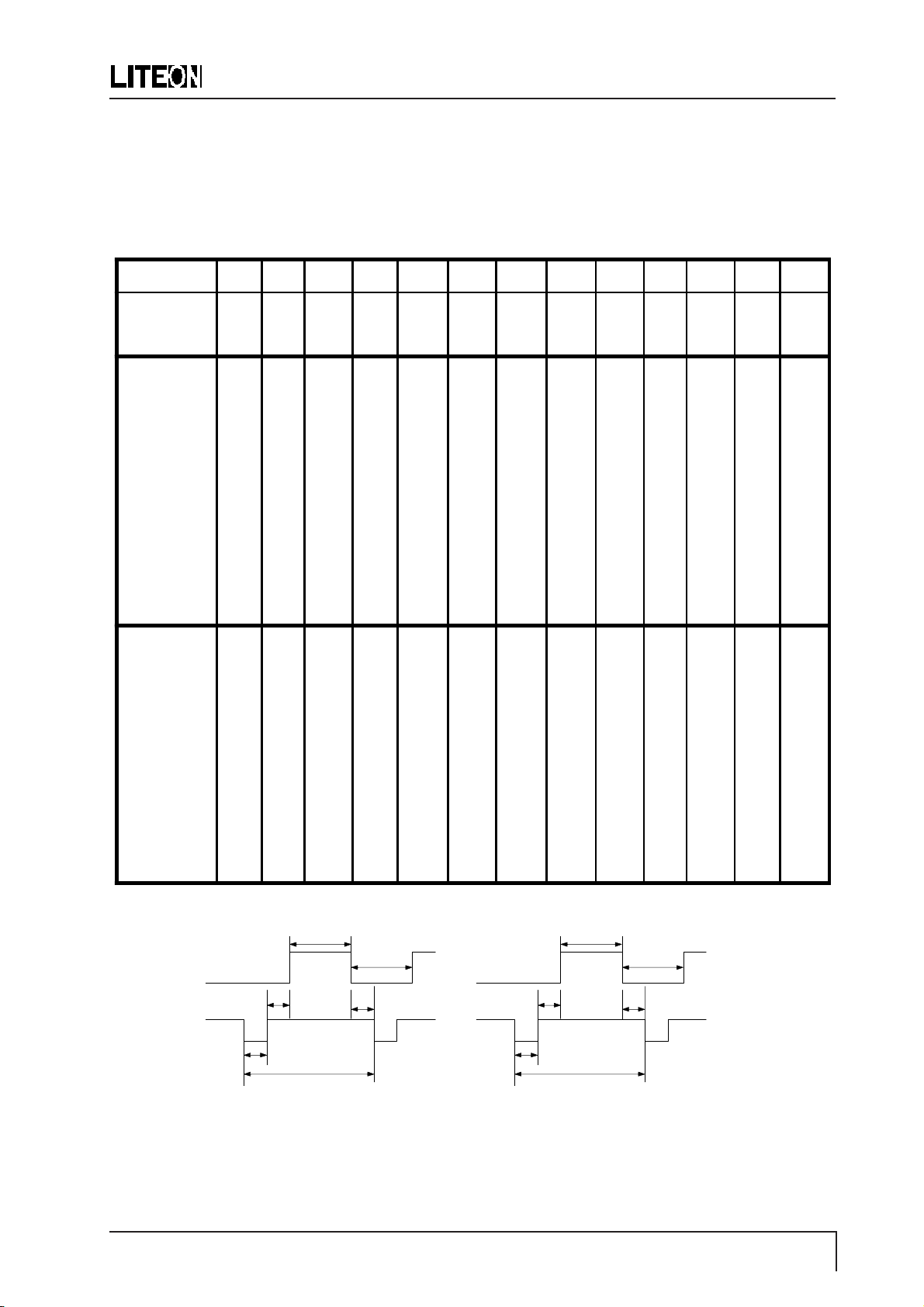
2-3 Timing Chart
This section describes the timings that the computer industry recognizes as standard for computer-generated
video signals.
T able 2-2. Timing Chart
Mode 1 2 3 4 5 6 7 8 9 10 11 12 13
H. D ots 720 640 640 800 640 640 800 1024 800 1024 1024 1280 1024
V. D o t s
H-freq (kHz) 3 1. 47 31.47 3 5 37.88 37.5 43. 3 46.8 4 8. 36 53.67 56.48 60.02 64.34 68.68
Sync Polarity ---+ - - + ++++++
A pe riod us 31.78 31.78 28.57 2 6.4 26. 666 23.111 21.33 3 2 0.68 18.63 17. 71 1 6.66 15.55 14.56
B Blking us 6.356 6.356 7.407 6.4 6.35 5.33 5.172 4.923 4.409 4.053 3.657 3.589 3.725
C S ync us 3.81 3.81 2.116 3.2 2.07 1.556 1.616 2.092 1.138 1.813 1.219 0.972 1.016
D B.P. us 1.907 1.907 3.175 2.2 3.81 2.222 3.232 2.462 2.702 1.92 2.235 2.248 2.201
E Acti ve us
F F. P. us 0.636 0.636 2.116 1 0.51 1.556 0.323 0.369 0.569 0.32 0.203 0.374 0.508
V-freq (Hz) 70.08 59.95 66.667 60.32 75 85 75 60 85 70.07 75.03 60 85
Sync Polarity +--+- - + + +++++
O Period ms 14.27 16.68 1 5 16.58 13.33 11.764 13. 333 16.67 11.76 1 4.27 13.33 16.67 11.77
P B lking ms 1.557 1.43 1.286 0.739 0.533 0.67 0.533 0.786 0.578 0.673 0.533 0.642 0.582
Q Sy nc ms 0.064 0.064 0.086 0.106 0.08 0.069 0.064 0.124 0.056 0.106 0.05 0.047 0.044
400 480 480 600 480 480 600 768 600 768 768 1024 768
25.42 25.42 21. 164 20 20.32
17.778
16.162 15.75 14.22 13.65 13 11.96
10.836
R B.P. us 1.08 1.02 1.14 0.607 0.407 0.578 0.448 0.6 0.503 0.513 0.466 0.501 0.524
S Active us 12.71 1 5.25 13. 714 15. 84 12.8 11.09 3 1 2.8 15.88 11.18 1 3.6 12.8 1 6.03 11. 18
T F.P. us 0.413 0.35 0.086 0.026 0.026 0.023 0.021 0.062 0.019 0.053 0.017 0.094 0.015
Seperate Sync
H orizontal
C
E
Video
D
Sync
A
H.Parameters:
A: Period B : Blanking Time
C: Sync Width D: Back Porch
E: Active T ime F : Front Porch
Product Specifications
Vertical
B
F
I
V.Parameters:
G: Period H :Blanking Time
I: Sync Width J: Back Porch
K: Active T ime L : Front Porch
K
Video
J
Sync
G
H
L
Page 7
Page 10
A1770NSL/NST
2-4 Display Power Management Signal (DPMS)
Note: These power-saving states exceed the Environmental Protection Agency (EPA) Energy Star
requirements and the Video Electronics Standard Association (VESA) for Display Power
Management Signal (DPMS) .
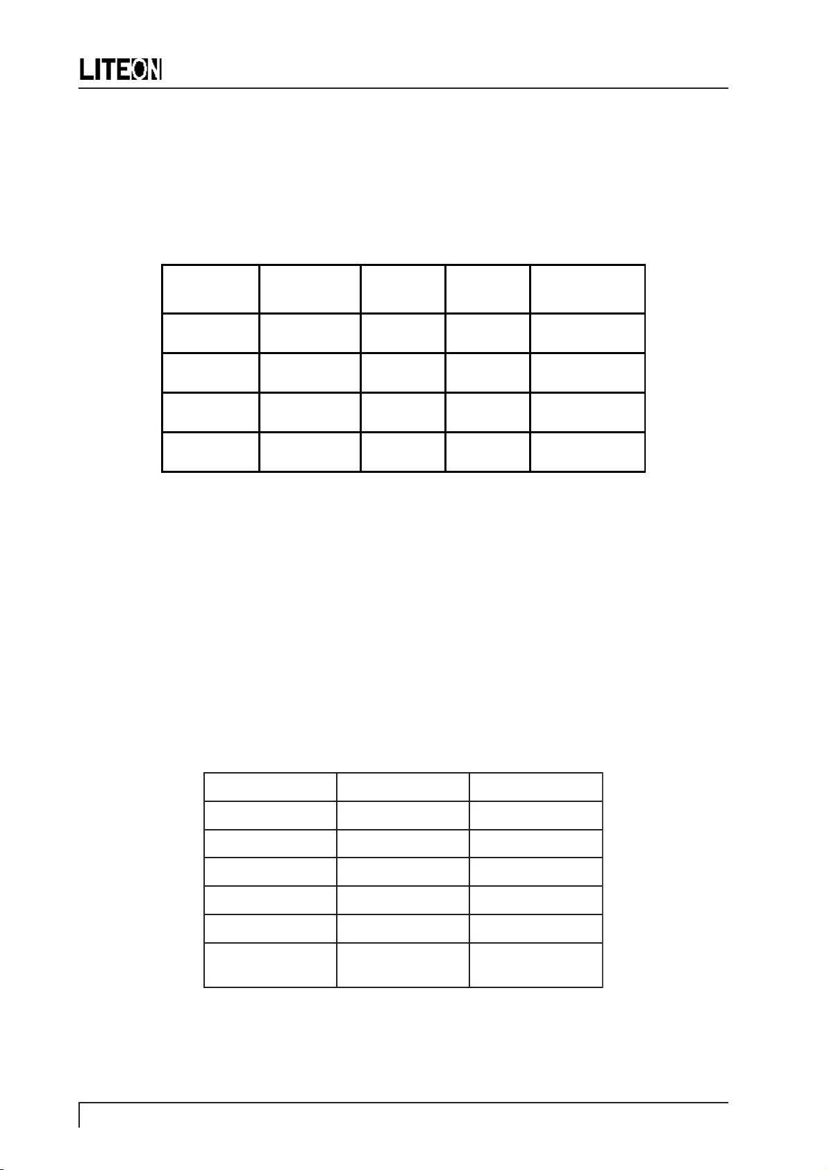
T able 2-3. Display Power Management Signal (DPMS)
State LED Color H-Sync V-Sync Power
Co nsumpti o n
ON Green Pulse Pulse Normal
STANDBY Yellow No Pulse Pulse <15 watts
SUS PEN D Ye llow Puls e N o P ulse < 15 wa tts
O FF Amb er N o Puls e No Puls e <8 wa tt s
2-6 TCO Version (Optional)
The monitor meets the TCO 92, NUTEK energy saving, electric and magnetic field requirements. Also it
is compliant with TCO 95 (optional) labelling scheme.
2-6-1 TCO 92 Version
The emission from magnetic and electric field must comply with the limits specified by the Swedish Board
for Measurement and T esting, commonly known as MPR 1990 recommendations. These limits are
summarized in the T able 2-4.
T able 2-4. TCO 92 Requirements
OCT/FLVOCT/FLE
dleiFcitengaMTn52Tn002
dleiFcirtcelEm/V1m/V01
egnaRycneuqerFzHk004~2zH0002~5
eulaVSMRSMR
ecnatsiDmc03mc03
citatsortcelE
laitnetoP
V005-/+V005-/+
The monitor is designed with selected CRT and carefully routed wires around CRT, make sure exactly the
same routing scheme is used for CRT replacement.
Product SpecificationsPage 8
Page 11
A1770NSL/NST
2-6-2 TCO 95 Version (Optional)
The TCO 95 scheme is for international and environmental labelling of personal computers. The labelling
scheme was developed as a joint effort by the TCO (The Swedish Confederation of Professional Employ
ees), Naturskyddsforeningen (The Swedish Society for Nature Conservation) and NUTEK (The National
Board for Industry and T echnical Development in Sweden).
1) Scope
TCO 95 touches on ergonomic qualities, emissions (electrical and magnetic fields), energy efficiency and
ecology (with demands for environmental adaptation for both the product and the production processes at
the manufacturing plant).
2) Environmental Requirements
The monitor abides by the environmental demands concerning restrictions on the presence and use of
heavy metals, brominated and chlorinated flame retardants, CFCs (freons), and chlorinated solvents,
among other things. The monitor is also recyclable.
3) Energy Requirements
The monitor also follows the energy requirements that, after a certain period of inactivity, the monitor
shall reduce its power consumption to a lower level in one or more stages.
4) Others
The monitor meets the strict environmental demands for the reduction of electric and magnetic fields,
physical and visual ergonomics and good usability.
Table 2-5. TCO 95 Visual Ergonomics
erutaeFdradnatSnoitpircseD
ytiraeniLsselro%1 ehtotderapmocsworrosnmulocfohtgnelniecnereffiD
ecnanimuLyalpsiD)tsaelta(2m/dc001
ecnanimuL
ytimrofinU
sselro1:7.1 ehtnihtiwecnanimulnimotxamehtneewtebsioitarehT
.aeraevitcaelohw
.rotinomehtforetnecehthguorhtshtgnelgnidnopserroc
Product Specifications
Page 9
Page 12
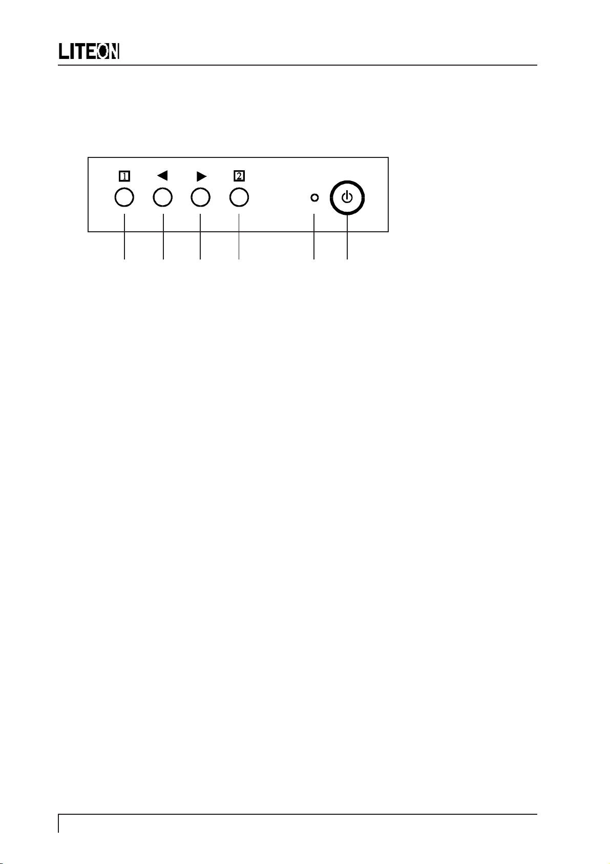
3 Control Location and Functions
(1) (2) (3) (6)(5)(4)
3-1 Front Panel
A1770NSL/NST
(1) Function Key
(2) Decrease Key
(3) Increase Key
(4) Select Key
(5) Power LED
(6) Power ON/OFF
3-2 Front Panel Keys Functions
1. Function Key: Display the main menu, and exit the adjustment screen and save adjustments.
2. Decrease Key: Scroll across main menu, highlighting control to be adjusted. Decrease value of selected
control. Toggle between Contrast and Brightness adjustment screens.
3. Increase Key: Scroll across main menu, highlighting control to be adjusted. Increase value of selected
control. Toggle between Contrast and Brightness adjustment screens.
4. Select Key: Press once to display adjustment screen. Press again, for some controls, to toggle between
controls shown in pairs on main menu.
5. Power LED: Display different modes (ON, standby, suspend or OFF) of the monitor by showing different
color for each mode.
6. Power ON/OFF: To turn the monitor ON and OFF.
3-3 Adjustment Procedure
1. Press (6) key to turn on the monitor.
2. At normal condition, press (1)on the front panel to activate the on-screen manager (OSM) menu. But to
enter the internal adjustment menu, keep pressing (1) & (4) key simultaneously and then press (6) key.
3. To select a user control, press (2) or (3) key repeatedly until the control is highlighted.
4. To adjust the value for particular control, press (4), then press the (2) or (3) key to obtain the desired
value. There are a few parameters that do not require any adjustment, like Manual Degauss, Memory
Recall.
5. Some controls are grouped in pairs on the main menu. Press (4) key to toggle between them.
6. To save your adjustments and exit screen, press (1) key. The menu will automatically clear out from the
screen if no keys are pressed within 30 seconds.
Page 10 Operation Theory
Page 13

A1770NSL/NST
4 Operation Theory
This is a fully digital controlled multi-sync color monitor that is compliant with DDC1 and 2B Plug and Play
VESA standard and offers the following main features.
4-1 Main Features
1. Simplified design with minimum components.
2
2. The NOVATEK NT68P61A processor-- that has I
brightness-- offers the functions for: (a) Contrast, (b) Brightness, (c) H-size, (d) H-position, (e) V-size, (f)
V-position, (g) Pincushion, and (h) Trapezoid.
C BUS controlled geometric correction, contrast and
In addition, it also offers more functions as: (a) Sync. processor, I/P and O/P, (b) Mute, (c) Power saving
2
- Suspend & Stand-By, (d) Power saving override, (e) DDC1/2B, (f) I
C Bus for auto-alignment through
signal cable (g) CS1/CS2/CS3/CS4 for linearity and size compensation.
3. Stores up to 14 factory preset modes and offers 8 user modes. There are 16 function icons at OSD. They
are controlled by
2 keys on front panel.
1
4. Powerful PHILIPS TDA4854 and TDA4866 present the following useful functions: (a) Pincushion, (b)
Trapezoid, (c) V-Position, (d) V-Size, (e) Vertical’ s “C” and “S” correction -- factory adjust, (f) Pincushion’ s
V. position correction, (g) Corner correction -- factory adjust, (h) Pincushion unbalance correction -factory adjust, (i) Parallelogram distortion -- factory adjust, (j) Moire cancellation -- factory adjust, (k) Xray protection, and (l) Full horizontal and vertical auto sync capability.
5. Software controlled auto shut off function activated if fH < = 29 kHz and fH > = 70 kHz.
6. Full range AC input and simplified line filter design.
4-2 Microcontrol Section
1. This monitor uses NOVATEK NT68P61 CPU. It contains a 6502 8-bit CPU core, 256 bytes of RAM
used as working RAM and stack area, 24k bytes of OTP ROM, 14-channel 8 bit PWM D/A converter,
2-channel A/D converters for key detection saving I/O pins, internal H. sync and V. sync signals processor
providing mode detection, and an I2C bus interface. When H/V sync through D-Sub signal cable enter pin
39 and pin 40, the CPU performs frequency / polarity detection and calculate and send to H/V sync OUT.
Then CPU reads the data from I703 and transfer to device 4854 and some DAC in CPU, above operation
takes about 500 ms.
2. There allowed 14 factory preset modes and 8 user modes. There are 8 functions, Contrast, Brightness, H.
Size, H. Position, V. Size, V. Position, Pincushion, and Trapezoid, all controlled by OSD icon which can
be adjusted by user.
3. The pin 24 and pin 25 are used for A TE function. When CPU receives C6 as slave address, it will operate
in ATE mode which is used for auto-alignment. After alignment the data will be stored in I703.
4. The user control parameters are selected by OSD icons, through
2 keys, they are detected by
1
sensing the voltage through R710, R740, R711, R743, R741, R711 to pin 13 and 14 of I701.
4-3 Deflection Section
1. I2C -- autosync deflection controller is TDA4854.
2. The TDA4854 is a high performance and efficient solution for autosync monitors. All functions are
controllable by I
control all functions.
Operation Theory Page 11
2
C bus. SDA and SCL signals come from microprocessor feed to pin 19 and pin 18 to
Page 14

A1770NSL/NST
4-3-1Horizontal Section
1. The oscillator is driven by the currents in R419 and R420. The minimum oscillator frequency is determined
by R419 and the maximum frequency is determined by R420.
2. Horizontal sync comes into pin 15 through R318. And horizontal flyback pulse comes into pin 1 through
R401 and by pass filter C403 from pin 9 of FBT and C453, R4C2, Q414, R4C3 for AFC loop.
3. Horizontal driver (pin8) O/P to Q401 via C410.
4-3-2 Vertical Section
1. V ertical sync comes into pin 14 through R317.
2. The free running frequency is determined by R301 and C301.
4-3-3 Vertical O/P section
1. The differential output currents from pin 13 of Vout1 and pin 12 of Vout2 can be directly coupled to the
vertical deflection booster pin 1 and pin 2 of TDA4866.
2. The TDA4866 has two output stages which are current driven in opposite phase and operate in combination
with the deflection coil in a full bridge configuration.
3. This IC is powered by two sets of positive voltage. (+12V at pin 3, +50V at pin 7).
4-3-4 E-W/T rapezoid and H. Width Contr ols
1. The horizontal O/P stage uses diode modulator D419, D423, C411, C412, L409 and C418 for East-West
(Pincushion) Trapezoid and H. width controls.
+
2. The scan current is determined by B
is accomplished by Darlington pair Q418 and Q419 by coupling a parabola waveform from pin 11 of
TDA4854. The H. width / corner and trapezoid correction are also accomplished by this pin 11. The DC
level controls H. size. The AC level is combined with side pin and trapezoid corners functions.
minus Vm ( the voltage of C418) values and the pincushion control
4-3-5 X-Ray Protection
1. To avoid X-ray hazard, a DC voltage generated by pin 6 of FBT and rectified by D408, C432 and divided
by R403, R404 and R405 come into pin 2 of TDA4854.
2. If this voltage is higher than 6.39 V, then TDA4854 will be activated to float HUNLOCK (pin17), H.
DRV( pin 8), B DRV (pin 6), VOUT1 (pin 12), VOUT2 (pin13). After that all deflection circuit stop
working.
4-3-6 G1, Blanking and Brightness
1. The vertical blanking signal comes from two ways. One is from pin 8 of I301 (TDA4866), the other is
from vertical sync (pin 32 of I701). These two positive vertical pulses through Q406 amplified and converted
into negative pulse and sent to G1 for vertical blanking.
2. In protection mode or an out-of- range situation HUNLock will send 5 V pulse to saturate Q406 and to
cutoff Q407, then G1 will go down to -140V. During the mode change, Mute acts as same as HUNLock’s.
3. The brightness is controlled by CPU pin 1 through PNP transistor Q407. The lower control voltage
causes Q407 conducts harder to get brighter raster and a higher control voltage causes Q407 conducts
lighter to get lower brightness.
Page 12 Operation Theory
Page 15

A1770NSL/NST
4-3-7 Contrast Section
1. Contrast is controlled by I701 through I2C bus to I501 (TDA4886) directly.
2. Beam current is detected through T402 (FBT) pin 7, C429, VR401, R460, and detected voltage feeding
into R461, R4F1, Q410, R430, R469, R524 to control I501 pin 24 voltage. When I501 pin 24 voltage drops
below 5V, the ABL function will happen.
4-3-8 H/V size breathing compensation
1. Beam current is sensed as above section (4-3-7 item 2) and this voltage routes through R458, C460,
Q409, R436, R459, then through R418 to I401 pin 31 for H. size compensation, through R302 to I401 pin
21 for V size compensation.
4-3-9 Dynamic focus circuity
The dynamic focus is applied to improve the corner focus performance, it includes horizontal and vertical
dynamic focus.
1. Horizontal and vertical dynamic comes from I401 pin 32 and amplified through C450, R499, Q431, Q404,
Q403, R437 and feed to FBT dynamic focus pins.
2. This amplifier need 800V voltage supply, it comes from FBT pin 2 and rectified through R4C6, D422 and
C448.
4-4 Power Supply Section
4-4-1 AC Rectifier
The circuit can accept 90 V to 264 V AC input through D801~D804 bridge diodes and C808 filtering to get
DC 126 V~364 V for power conversion in T802.
4-4-2 Line Filter
It consists of C801, C802, C803, C816, C852, C853, C807 and T801 and meets EMI regulation.
4-4-3 Power LED Status
1. The LED has 3 leads with common cathode to emit green and amber color light for different power
saving indications. It is controlled by CPU.
2. Normal : Green light
Amber LED is off because CPU pin 35 is high and pin 34 is low, only green LED is turned on.
3. Standby / Suspend : Y ellow light
CPU pin 34 and pin 35 are low, then green and amber LED are turned on. That is yellow.
4. Off Mode : Amber light
CPU pin 34 is high and pin 35 is low, then green is off and amber is illuminated.
Operation Theory Page 13
Page 16

A1770NSL/NST
4-4-4Auto Degaussing
When S701 turns on, pin 19 of I701 will send a signal to Q802 and turns on RL801 for degaussing. After 4
seconds, it will turn off RL801 automatically.
4-4-5 PWM Control
1. Start Up
The I801 (MC3842) gets power from R807, R873, C812 and pin 7 voltage reaches 16 V for starting up.
The I801 starts oscillation at 22 kHz, sawtooth on pin 4 and pin 6 output to drive Q803/T802. Once Q803
switching on, D806, C804 set up an 15 V to keep I801 working through D808 auxiliary voltage.
2. Regulation
The DC O/P voltage is proportional to the auxiliary voltage, so I801 pin 2 senses the feedback voltage
from the divider R802, R823, VR801 and R821 to compare with the built-in 2.5 volts reference voltage for
error amplifier operation. Finally pin 6 can modulate the different duty cycle by VR801 setting to achieve
regulation purpose.
4-4-6 Synchronization
1. Normal Mode
The sync pulse from FBT (31 kHz~69 kHz) via C815, R826, D824, C814 and R816 to pin 4 of I801 to
keep I801 synchronized with horizontal sync input frequency.
2. Power Saving Modes: Standby/Suspend
Because there is no pulse from FBT, so the free-run frequency is decided by R815 and C814 and the
SMPS works at 22 kHz.
3. Override
The horizontal free run frequency is about 62.5 kHz under override condition, SMPS is synchronized to
this frequency.
4-4-7 O.V.P.
If the auxiliary voltage is higher than zener voltage ZD807 (18 volts) and makes pin 3 of I801 higher than
1 V, pin 6 duty cycle is limited to have the OVP activated.
4-4-8 O.P.P.
The excess current of T802 through R813, R865 and R864 can develop enough voltage on pin 3 then limit the
power delivered because the pin 6 duty cycle is limited too.
4-4-9 Step Up Power Supply For FBT
1. The B+ of FBT is proportional to horizontal frequency, that is the higher frequency, the higher voltage.
The basic voltage is 55 volts from T802 pin 3 via D840, L812 and the gate control of Q807 comes from
I401 pin 6 via Q808, Q809 and D821. The duty cycle is controlled by C843, C462, R489, R846 and R856,
R857, R858 VR802 combination ratio.
2. The regulation and boost up (from 68 V to 155 V or more, on demand). The H.V. is set at 25 kV (zero
beam) by VR802 which senses the secondary O/P from FBT. The booster comprises Q807, L801, D820,
C425 and I802 to offer the required B+ for different frequency modes.
Page 14 Operation Theory
Page 17

A1770NSL/NST
4-5 V ideo Amplifier Section
1. RGB signal inputs are terminated by R501, R531 and R561 then pass through the coupling capacitors
C503, C533 and C563 to the IC501 TDA 4886 preamplifier.
2
2. The amplifier RGB signals (0~3 Vpp) are adjusted by I
comes from pin 16 of TDA4854 to set up the equal clamp level.
3. The video output stages are amplified by I901 (LM2407).
4. The RGB cathodes cut off are adjusted by VR910, VR940 and VR970.
5. Under override condition, “NO SIGNAL” will show on the screen.
C bus from I501, pin 5 is for clamp pulse which
4-6 OSD (On Screen Display) Circuit
1. The I502 HTV018-08 is OSD IC. The OSD signals are worked by positive vertical pulse from I701 pin 32
that goes through R517 to I502 pin 10, and positive horizontal pulse from T402 pin 9 goes through C453,
R422, Q414, R4C3 to I502 pin 5. CPU I701 pin 26, 27 (I2C bus) transfers information to I502 pin 7, 8.
2. The OSD R. G. B signals and blanking signal are terminated at I502 pin 15,d 14, 13, and 12 to I501 pin 2,
3,4, and 1, then the OSD picture appears.
Operation Theory Page 15
Page 18

A1770NSL/NST
5 Alignments and Adjustments
This section of the service manual explains how to make permanent adjustments to the monitor settings.
5-1 General Adjustments
5-1-1Adjustment Conditions
a) Power Supply
Apply AC 115 V or 220 V
b) Warm-up Time
The monitor must be powered on for 15 minutes before starting any alignment, but requires 30 minutes of
warm-up time for convergence adjustment.
c) Signal Input
1. Video: RGB Analog, 0.7 Vp-p, positive
2. Synchronization: Horizontal and vertical TTL signal, separate, positive or negative
3. All adjustments should be made using a signal of FH = 31.468 kHz, FV = 60 Hz, unless otherwise
defined.
5-1-2 Equipment Required
The following equipments are necessary for adjustment procedures:
1. Volt-ohm-A meter (Sanwa FD-750C or equivalent)
2. 30 kV high voltage probe (HP34111A)
3. Oscilloscope (TEK2235 or equivalent)
4. Minolta Color Analyzer II
5. Signal generator (IBM PC with proper display cards or Chroma 2000)
6. Screwdriver
5-1-3 Switching Power Supply and Regulator Adjustment
a. The regulated B+ control has been preset in the factory and needs no adjustment. However, if any repair
is made on the power supply section, the following readjustment procedures are recommended:
1. Allow the monitor to warm-up for about 15 minutes.
2. Apply XGA (1024 x 768 @ 68 kHz/85 Hz) signal to the monitor.
3. Connect a DC voltage meter to D814 “-” (on the control PCB), and adjust VR801 for 12.8 +
0.2 V DC
4. If a fuse is broken during adjustment, remember to replace it with the exact same type of fuse.
b. If necessary, follow the following procedures to enter the factory mode.
1. Short ATE pin to GND wire and put COM wire short COM and A TE 1 at power off condition.
2. Press both
Now, we are in the factory preset mode.
3. When turns the power off, this monitor will go back to normal mode (user mode).
4. When finish the normal alignment. Open ATE pin and change GND wire to GND 1, put COM wire to
short COM and DDC.
key and 2 key simultaneously then power on.
1
Page 16 Alignments and Adjustments
Page 19

A1770NSL/NST
5-2 Alignment Procedures
5-2-1 High Voltage Adjustment
CONDITION
Display image : Crosshatch pattern
PROCEDURE
Connect DC meter to TP3 and adjust VR802 to obtain a DC voltage of 152 ± 1V DC for CPT CRT M41AGE
93x46C or M41AGE83x46C.
5-2-2 Screen and White Balance Adjustment
CONDITION
Press
and 2 buttons simultaneously when switching the power On.
1
Bias VRs : VR910, VR940, VR970
Display image : No video
PROCEDURE
1 Raster color setting
1-a. Set brightness (OSD Icon) to -30 V at G1 and 600 V at G2.
1-b Adjust VR910, VR940 and VR970 to maximum.
1-c Adjust VR940 to y=0.9 ± 0.2 FL.
1-d Adjust VR910 to get x=280 ± 5 and VR970 to get y=280 ± 5
1-e Adjust brightness to raster just distinguish.
CONDITION
Display image : 50 mm x 50 mm white block pattern
PROCEDURE
0
2 6500
K color temperature setting
2-a. Set brightness to cutoff and contrast to maximum.
2-b Move cursor on OSD to choose color temperature icon.
2-c. Press
key to G gain then adjust G gain = 68 value, then adjust B, R to y=329±5, x=313±5.
2
2-d Adjust contrast to set y=40±2FL
2-e Check x=313±5, y=329±5.
0
3 9300
K color temperature setting
3-a. Set brightness to cutoff and contrast to maximum.
3-b Move cursor on OSD to choose color temperature icon.
3-c. Press
key to G gain then adjust G gain = 71 value, then adjust B, R to y=311±5, x=281±5.
2
3-d Adjust contrast to set y=40±2FL
3-e Check x=281±5, y=311±5.
4 Full white ABL setting
CONDITION
Display image : full white pattern
4-a Set brightness to cutoff and contrast to maximum.
Alignments and Adjustments
Page 17
Page 20

A1770NSL/NST
4-b. Adjust VR 401 to y=28FL ±2FL.
4-c. Check the white balance at 5FL and 28FL.
4-d. Repeat all the procedures in 5-2-2 section until the best white balance is obtained, then power off.
5-2-3Focus Adjustment
CONDITION
Display image : “e” character pattern
PROCEDURE
1. Set brightness to cutoff and contrast to maximum.
2. Adjust top VR at T402 (static focus VR) to make vertical line clear.
3. Adjust center VR at T402 (dynamic focus VR) to make horizontal line clear.
4. Repeat above procedures to get best focus.
5-2-4Dynamic focus Adjustments
1. Horizontal dynamic focus set Hf=340V in phase (compare with video signal).
2. V ertical dynamic focus set Vf=160V in phase.
5-2-5Static Convergence Adjustments
Static convergence involves alignment of the red, blue and green lines in the center area of the display.
Note : The monitor requires 30 minutes of warm-up time for convergence adjustment.
CONDITION
Display image : Crosshatch pattern
Warm-up Time : 30 minutes
PROCEDURE
1. Set brightness and contrast to display a well-defined pattern.
2. Ensure the convergence magnet rings are correctly positioned on the CRT.
Page 18 Alignments and Adjustments
Page 21

Figure 4-1. Convergence Magnets on the CRT
1
11
+
A1770NSL/NST
P
CRT
FRONT
8 7 6 5 4 3 2
10
9
1) Setup Bolt 2) Bow Magnet 3) Band 4) 2-Pole Magnet
5) Spacer 7) Spacer
9) Holder
6) 4-Pole Magnet
8) 6-Pole Magnet
11) Tabs10) Band
3. Rotate the individual rings of 4-pole convergence magnets by changing the spacing between the 2 tabs to
converge the vertical red and blue lines at the center of the screen.
4. Rotate the pair of rings of 4-pole convergence magnets by maintaining spacing between the 2 tabs to
converge the horizontal red and blue lines at the center of the screen.
5. Rotate the individual rings of 6-pole convergence magnets by changing the spacing between the 2 tabs to
converge the vertical red, blue and green lines.
6. Rotate the pair of rings of 6-pole convergence magnets by maintaining spacing between the 2 tabs to
converge the horizontal red, blue and green lines.
7. Repeat the steps from 3~6 until the best convergence is obtained.
Figure 4-2. 4-pole and 6-pole Magnets Movement
Red/
Blue Gree n
6-pole magn ets
movement
Blue
Red
Blue Red
Red/
Blue
Green
4-pole magn ets
movement
Note : The 4-pole magnets and the 6-pole magnets interact, making dot movement complex.
Alignments and Adjustments
Page 19
Page 22

A1770NSL/NST
5-2-6 Degaussing
Degaussing is required when poor color impurity appears on the screen. This monitor uses an automatic
degaussing circuit that is activated when the power is on. The automatic degaussing will be fully functional
again after the monitor has been in operation for 20 minutes.
The degaussing effect is confined to the picture tube since the coils are mounted at the back of the tube.
Should any part of the chassis or cabinet becomes magnetized, it is necessary to degauss the affected area
with a manual degaussing coil.
5-2-7 Manual Degaussing
1. Apply line voltage to the degaussing coil and move it in a rotary motion over the front, sides, and top of the
monitor. The coil should be kept away from the rear of the monitor to avoid damaging the magnetic neck
components.
2. Slowly rotate and move the coil away from the monitor to about 6 feet beyond the point where no effect
on the CR T will be noticeable.
For proper degaussing, it is essential that the field be gradually reduced by moving the coil slowly away from
the monitor. The degaussing coil must never be shut off or disconnected while near the monitor, as this would
introduce a strong field instead of canceling the effect of the stray fields.
Page 20 T roubleshooting
Page 23

6 T roubleshooting
6-1 No Raster
A1770NSL/NST
No Raster
Measure
voltage of B+ at
T402 pin 3 on
PWB-MAIN
0 V
Short Circuit
at load?
Yes
Check DC B+ line,
Q808, Q809, Q402
(68 V, 31.5 kHz)
Check voltage of
No
Check AC I/P
on C808
I801, Q803,
R814, R813,
R818, R811,
ZD807, ZD801
cathode, heater,
Grid 1, Grid 2,
Yes
Check
Normal
etc.
No
D801, D802,
D803, D804,
T801, R804
High
(75 V or more)
Check I401,
R858, R857,
R856, VR802
Check
T roubleshooting
Page 21
Page 24

6-2 OSD Abnormal
A1770NSL/NST
OSD Abnormal
Check I502
missing?
No
Check R520,
R578, R579
OK?
Yes
Check P502B
OK?
Yes
Yes
No
No
Put on
I502
Replace them
Replace it
Replace I502
Page 22 T roubleshooting
Page 25

6-3 Function Key Abnormal
Function Key Abnormal
A1770NSL/NST
Check I701 and
I703 missing?
No
Power
ON/OFF again and
check X701,
oscillator OK?
Yes
Check
I703 EEPROM
content OK?
Yes
Yes
No
No
Put on
I701, I703
Replace X701
Replace I703 or
do ATE again
T roubleshooting
Replace I701 and
check uP OK?
No
Check
pin 5 of I701
is 5V?
No
Replace R842, Q805
Yes
Yes
Replace I701
Check
Q703, Q704
Page 23
Page 26

6-4 No Vertical Scan (Raster is one horizontal line)
No Vertical Scan
A1770NSL/NST
Check voltage of
pin 3 is 12V, pin 7
is 50V?
Yes
Check
pin 6 O/P waveform
at I301
Normal
Check
pin 1, 2, 9 of I401
waveform
No
Abnormal
Ckeck or replace
I301.
Replace I301
Still no vertical scan
Check or replace CRT
Page 24 T roubleshooting
Page 27

6-5 Out of Horizontal Synchronization
Out of Horizontal
Synchronization
A1770NSL/NST
Horizontal
sync present at
pin 15 of I401
Yes
Check
I401 pin 8 H output
frequency
Yes
Check Q401, T401,
Q402, R424,
R425, D401
6-6 Out of Vertical Synchronization
Out of Vertical
Synchronization
No
No
Ckeck or replace
the signal cable
or I701
Check or
replace the
signal cable
or I701
Vertical sync
present at
pin 14 of I401
Yes
Check
I401 pin 24 ramp
frequency
Check C301
Recommended Spare Parts List
No
Ckeck signal cable
& vertical sync
input & I701
Page 25
Page 28

6-7 R.G.B. Video Amplifier Abnormal
RGB Video AMP Abnormal
A1770NSL/NST
Check
waveform at I501 pin 16, 19
and 22
Yes
Check
I901 pin1, 3 & 5 collector
voltage (normally about 72V)
& waveform
Yes
Video signal present at the
pin of the CRT R.G.B.
Cathode
Yes
Check or replace the
No
signal cable or I501
No
Check I901
Defective cut-off circuit
(DC restore)
Page 26 T roubleshooting
Page 29

A1770NSL/NST
7 Recommended Parts List
Note: The components identified by “ “ mark are critical for X-ray safety. Replace these with
only the same parts specified.
No. Locat ion Part Number Desc ription
1 C417 6326215442 MPP uF 0.15 250V J F P=15 HJ C
2 C808 6312622126 ALU uF 220 400V F 85C 25x40
3
4 D814 6412017900 DIODE RL3 3.5A/350V SANKEN
5 D815 6412004117 DIODE UF2004M T52 2A/ 400V 50nS
6 D820 6412002017 DIODE UF3004M T52 3A/400V 50nS
7 F801 6851004050 FUSE TIME LAG 5ST4 4A/250V
8 I301 6442012300 IC TDA4866 9P (PHILIPS)
9 I401 6442020700 IC TDA4854 32P SDIP (PHILIPS)
10 I501 6442021500 IC TDA4886 24P SDIP (PHILIPS)
11 I701 6448012200 IC NT68P61A 40P PDIP OTP NOVAT
12 I703 6448007900 IC 24C04A/P (MICROCHIP)
13 I801 6442006020 IC UC3842BN 8P PDIP ( ST)
14 L404 6111504130 COIL CHOKE 5mH K DR10x16 LY3B
D801 D802
D803 D804
6412011307 DIODE 1N5406 T52 3A/600V
15 L405 6119005200 COIL LINEAR TLN-1052
16 L406 6111686131 COIL CHOKE 68uH K DRWW10x16
17 L409 6111105131 COIL CHOKE L=105uH K DRWW16x18
18 Q402 6421004400 TR NPN 2SC5386 (TOSHIBA)
19 Q420 Q421 6426001800 FET N-CHNL IRFS630 TO-220F
20 Q430 Q807 6426006400 FET N- CHNL IRFS630A SAMSUNG
21 Q803 6426006800 FET N-CHNL SS S10N60A SAMSUNG
22 R403 6224211024 MF KOHM 11 1/4W F T2 6
23 R404 6224213024 MF KOHM 13 1 /4 W F T26
Recommended Spare Parts List
Page 27
Page 30

No. Location Part N umbe r De s cription
A1770NSL/NST
24
25
26
27
28
29
30 T801
31 T802
32 X701
R405 6224130114 MF KOHM 3.01 1/8W F T26
R803 6203090002 POSISTOR 9 O HM Q 2PINPITC H=10
R804 6201100012 THERMISTOR 10 OHM 3A P=7.5 TKS
R818 6220327852 FS OHM 0.27 1W J HO R
T401 6135000801 XFRMR HOR DRIVE THD- 1008A EI19
T402 6133070020 FBT TFB-7002 FEA766 SAMPO
6138001601 LINE FILTER TLF- 1016A 16mHET28
6131060700 XFRMER PWR TPW- 1065 EE42/15DEI
6449000710 CRYSTAL 8MHz TOP8.000 30pF TOP
Page 28 Recommended Spare Parts List
Page 31

8 Block Diagram
P501
RG
R
GG
G
BG
B
H
V
5V
SG
SDA
SCL
O/R
LED
DDC
I704
OSD
BLK
KEY
CONTROL
S702
R
G
B
RGB
O/R
V
H
SDA
SCL
I501
PRE AMP
TAD4886
R
G
B
12V
I701
NT68P61A
OSD
MTV018
ABL
I901
Video AMP
LM 2407
SDA 1
SCL 1
A1770NSL/NST
Q901
R BUFFER &
DC RESTORE
Q931
G BUFFER &
DC RESTORE
12V
V
H
B BUFFER &
DC RESTORE
BLANKING
CKT Q302
I401
TDA4854
Q961
G1
ABL
BRIGHTNESS
CONTROL &
SPOT KILLER
H
DRIVER
SCL1
SDA1
V-LBL
V-TTL
H
OUT
H-TLB
GND
5V
6.3V
12V
80V
145V
GND
P503
24.5KV
HFLB
-130V
570V
FBT
6.6KV
145V
DIODE
MODULATE
RESET
CKT
E2PROM
I703
LINE
FILTER
BRIGHTNESS
DEG
CKT
BRIDGE
DIODE
5V
Q805
LOW VOLTAGE
DROP DOWN
SMPS
POWER
O/P
TRANS
T802
VERTICAL
O/P
I301
STEP
UP
CKT
dynamic
foucus
I802
+H
-H
+V
D.Y
-V
800V
TDA4866
XRP
12.5V
Q813
Q811
7V
80V
Block Diagram
Page 29
Page 32

Page 33

Page 34

Page 35

Page 36

Page 37

LITE-ON TECHNOLOGY CORP.
5 F, No. 16, Sec. 4, Nanking E. Road, Taipei, Taiwan
T el: 886-2-25706999Fax: 886-2-25706888
URL:// www.liteontc.com.tw
Printed in Taiwan
 Loading...