

Page 1
■
■
■
■
■
■
■
Single-channel: 6N137, HCPL-2601, HCPL-2611 Dual-Channel: HCPL-2630, HCPL-2631 High Speed-10 MBit/s Logic Gate Optocouplers
July 2005
Single-channel: 6N137, HCPL-2601, HCPL-2611
Dual-Channel: HCPL-2630, HCPL-2631
High Speed-10 MBit/s Logic Gate Optocouplers
Features
■
Very high speed-10 MBit/s
■
Superior CMR-10 kV/µs
■
Double working voltage-480V
■
Fan-out of 8 over -40°C to +85°C
■
Logic gate output
■
Strobable output
■
Wired OR-open collector
■
U.L. recognized (File # E90700)
Description
The 6N137, HCPL-2601/2611 single-channel and HCPL-2630/
2631 dual-channel optocouplers consist of a 850 nm AlGaAS
LED, optically coupled to a very high speed integrated photodetector logic gate with a strobable output. This output features
an open collector, thereby permitting wired OR outputs. The
coupled parameters are guaranteed over the temperature range
of -40°C to +85°C. A maximum input signal of 5 mA will provide
a minimum output sink current of 13mA (fan out of 8).
An internal noise shield provides superior common mode rejection of typically 10kV/µs. The HCPL- 2601 and HCPL- 2631 has
Applications
Ground loop elimination
a minimum CMR of 5 kV/µs. The HCPL-2611 has a minimum
CMR of 10 kV/µs.
LSTTL to TTL, LSTTL or 5-volt CMOS
Line receiver, data transmission
Data multiplexing
Switching power supplies
Pulse transformer replacement
Computer-peripheral interface
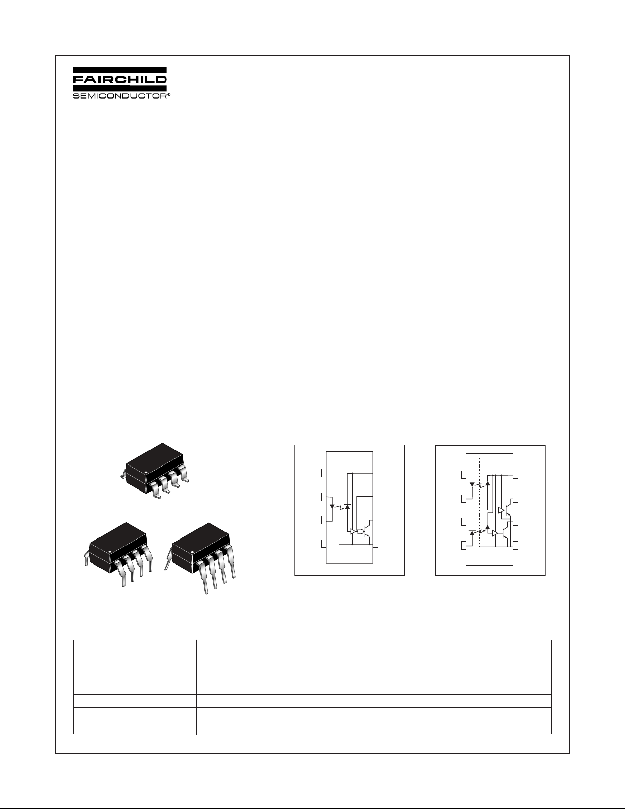
PackageSchematic
N/C
1
8
+
2
1
V
F
_
3
N/C
4 5
V
8
CC
V
7
E
V
6
O
GND
+
1
V
F1
_
2
_
3
V
F2
+
4 5
V
8
CC
V
7
01
V
6
02
GND
8
1
8
1
6N137
HCPL-2601
HCPL-2611
Truth Table (Positive Logic)
Input Enable Output
H H L
L H H
H L H
L L H
H NC L
L NC H
A 0.1µF bypass capacitor must be connected between pins 8 and 5. (See note 1)
©2005 Fairchild Semiconductor Corporation
Single-channel: 6N137, HCPL-2601, HCPL-2611 Dual-Channel: HCPL-2630, HCPL-2631 Rev. 1.0.3
1
HCPL-2630
HCPL-2631
www.fairchildsemi.com
Page 2
Single-channel: 6N137, HCPL-2601, HCPL-2611 Dual-Channel: HCPL-2630, HCPL-2631 High Speed-10 MBit/s Logic Gate Optocouplers
Absolute Maximum Ratings
(T
= 25°C unless otherwise specified)
A
Parameter Symbol Value Units
Storage Temperature T
Operating Temperature T
Lead Solder Temperature T
STG
OPR
SOL
EMITTER
DC/Average Forward Single Channel I
F
Input Current Dual Channel (Each Channel) 30
Enable Input Voltage
Not to exceed V
by more than 500 mV
CC
Reverse Input Voltage Each Channel V
Power Dissipation Single Channel P
Single Channel V
E
R
I
Dual Channel (Each Channel)
DETECTOR
Supply Voltage V
Output Current Single Channel I
CC
(1 minute max)
O
Dual Channel (Each Channel) 50
Output Voltage Each Channel V
Collector Output Single Channel P
O
O
Power Dissipation Dual Channel (Each Channel) 60
-55 to +125 °C
-40 to +85 °C
260 for 10 sec °C
50 mA
5.5 V
5.0 V
100 mW
45
7.0 V
50 mA
7.0 V
85 mW
Recommended Operating Conditions
Parameter Symbol Min Max Units
Input Current, Low Level I
Input Current, High Level I
Supply Voltage, Output V
Enable Voltage, Low Level V
Enable Voltage, High Level V
Low Level Supply Current T
FL
FH
CC
EL
EH
A
Fan Out (TTL load) N 8
*6.3mA is a guard banded value which allows for at least 20% CTR degradation. Initial input current threshold value is
5.0 mA or less.
0 250 µA
*6.3 15 mA
4.5 5.5 V
0 0.8 V
2.0 V
CC
V
-40 +85 °C
Single-channel: 6N137, HCPL-2601, HCPL-2611 Dual-Channel: HCPL-2630, HCPL-2631 Rev. 1.0.3
2
www.fairchildsemi.com
Page 3
/ ∆
Single-channel: 6N137, HCPL-2601, HCPL-2611 Dual-Channel: HCPL-2630, HCPL-2631 High Speed-10 MBit/s Logic Gate Optocouplers
Electrical Characteristics
(T
= 0 to 70°C Unless otherwise specified)
A
Individual Component Characteristics
Parameter Test Conditions Symbol Min Typ** Max Unit
EMITTER
Input Forward Voltage T
Input Reverse Breakdown Voltage (I
Input Capacitance (V
Input Diode Temperature Coefficient (I
DETECTOR
High Level Supply Current Single Channel (V
CC
Dual Channel (V
Low Level Supply Current Single Channel (V
= 5.5 V, I
CC
Dual Channel (V
Low Level Enable Current (V
High Level Enable Current (V
High Level Enable Voltage (V
Low Level Enable Voltage (V
Switching Characteristics
CC
(T
= -40°C to +85°C, V
A
CC
CC
CC
= 5.5 V, I
= 5.5 V, I
AC Characteristics Test Conditions Symbol Min Typ** Max Unit
Propagation Delay Time
to Output High Level
Propagation Delay Time
to Output Low Level
Pulse Width Distortion (R
Output Rise Time
(10-90%)
Output Rise Time
(90-10%)
Enable Propagation Delay
Time to Output High Level
(R
Enable Propagation Delay
Time to Output Low Level
(R
Common Mode Transient
Immunity (at Output High
Level)
6N137, HCPL-2630
HCPL-2601, HCPL-2631
HCPL-2611 |VCM| = 400V 10,000 15,000
Common Mode Transient
Immunity (at Output Low
Level)
6N137, HCPL-2630 |VCM| = 50V (Peak)
(RL = 350Ω) (IF = 7.5 mA, VOL (Max.) = 0.8V |CML| 10,000 V/µs
HCPL-2601, HCPL-2631 (TA = 25°C)(Note 11)(Fig. 14) 5000 10,000
HCPL-2611(TA = 25°C) |VCM| = 400V 10,000 15,000
(R
(R
= 350 Ω , C
L
= 350 Ω , C
L
= 350 Ω , C
L
= 350 Ω , C
L
= 350 Ω , C
L
(I
= 15 pF) (Note 8) (Fig. 13)
L
(I
= 15 pF) (Note 9) (Fig. 13)
L
(T
= 25°C) |V
A
(I
= 0 mA, V
F
(I
= 10mA) V
F
= 25°C 1.4 1.75
A
= 10µA) B
R
= 0, f = 1 MHz) C
F
= 10mA) ∆ V
F
= 5.5 V, I
= 5.5 V, V
= 5.5 V, V
= 10 mA)(Note 3) V
F
(R
(R
= 7.5 mA, V
F
= 7.5 mA, V
F
= 0 mA) I
F
= 0.5V) 10 15
E
= 10 mA) I
F
= 0.5V) 14 21
E
= 0.5V) I
E
= 2.0V) I
E
= 10 mA) V
F
= 5 V, I
CC
(Note 4) (T
= 15 pF) (Fig. 12) 100
L
(Note 5) (T
= 15 pF) (Fig. 12) 100
L
= 15 pF) (Fig. 12) |T
L
= 350 Ω , C
L
(Note 6) (Fig. 12)
= 350 Ω , C
L
(Note 7) (Fig. 12)
CM
OH
(R
= 350Ω) (Note 10)
L
= 25°C) T
A
= 25°C) T
A
= 15 pF)
L
= 15 pF)
L
= 3.5 V)
EH
= 3.5 V)
EH
| = 50V, (Peak)
(Min.) = 2.0V)
F
VR
IN
F
CCH
CCL
EL
EH
EH
EL
= 7.5 mA Unless otherwise specified)
F
5.0 V
T
A
-1.4 mV/°C
-0.8 -1.6 mA
-0.6 -1.6 mA
2.0 V
20 45 75 ns
25 45 75 ns
-
|
| V/µs
H
PHL
T
PLH
t
ELH
t
EHL
|CM
PLH
PHL
t
r
t
f
(Fig. 14) 5000
1.8 V
60 pF
710mA
913mA
0.8 V
335ns
50 ns
12 ns
20 ns
20 ns
10,000
10,000
Single-channel: 6N137, HCPL-2601, HCPL-2611 Dual-Channel: HCPL-2630, HCPL-2631 Rev. 1.0.3
3
www.fairchildsemi.com
Page 4
Single-channel: 6N137, HCPL-2601, HCPL-2611 Dual-Channel: HCPL-2630, HCPL-2631 High Speed-10 MBit/s Logic Gate Optocouplers
Transfer Characteristics (T
= -40 to +85°C Unless otherwise specified)
A
DC Characteristics Test Conditions Symbol Min Typ** Max Unit
High Level Output Current (VCC = 5.5 V, VO = 5.5 V)
(IF = 250 µA, VE = 2.0 V) (Note 2)
Low Level Output Current (VCC = 5.5 V, IF = 5 mA)
(VE = 2.0 V, ICL = 13 mA) (Note 2)
Input Threshold Current (VCC = 5.5 V, VO = 0.6 V,
VE = 2.0 V, IOL = 13 mA)
Isolation Characteristics (T
= -40°C to +85°C Unless otherwise specified.)
A
V
I
OH
I
FT
OL
100 µA
.35 0.6 V
3 5 mA
Characteristics Test Conditions Symbol Min Typ** Max Unit
Input-Output
Insulation Leakage
Current
Withstand Insulation Test Voltage (RH < 50%, TA = 25°C)
Resistance (Input to Output) (V
Capacitance (Input to Output) (f = 1 MHz) (Note 12) C
** All Typicals at VCC = 5V, TA = 25°C
NOTES
1. The V
tantalum capacitor with good high frequency characteristic and should be connected as close as possible to the package V
supply to each optoisolator must be bypassed by a 0.1µF capacitor or larger. This can be either a ceramic or solid
CC
GND pins of each device.
2. Each channel.
3. Enable Input - No pull up resistor required as the device has an internal pull up resistor.
4. t
5. t
6. t
7. t
8. t
9. t
10. CM
11. CM
12. Device considered a two-terminal device: Pins 1,2,3 and 4 shorted together, and Pins 5,6,7 and 8 shorted together.
-Propagation delay is measured from the 3.75 mA level on the HIGH to LOW transition of the input current pulse to the 1.5 V
PLH
level on the LOW to HIGH transition of the output voltage pulse.
-Propagation delay is measured from the 3.75 mA level on the LOW to HIGH transition of the input current pulse to the 1.5 V
PHL
level on the HIGH to LOW transition of the output voltage pulse.
-Rise time is measured from the 90% to the 10% levels on the LOW to HIGH transition of the output pulse.
r
-Fall time is measured from the 10% to the 90% levels on the HIGH to LOW transition of the output pulse.
f
-Enable input propagation delay is measured from the 1.5 V level on the HIGH to LOW transition of the input voltage pulse to
ELH
the 1.5 V level on the LOW to HIGH transition of the output voltage pulse.
-Enable input propagation delay is measured from the 1.5 V level on the LOW to HIGH transition of the input voltage pulse to
EHL
the 1.5 V level on the HIGH to LOW transition of the output voltage pulse.
-The maximum tolerable rate of rise of the common mode voltage to ensure the output will remain in the high state (i.e., V
H
> 2.0 V). Measured in volts per microsecond (V/µs).
-The maximum tolerable rate of rise of the common mode voltage to ensure the output will remain in the low output state (i.e.,
L
V
< 0.8 V). Measured in volts per microsecond (V/µs).
OUT
(Relative humidity = 45%)
(TA = 25°C, t = 5 s)
(V
= 3000 VDC)
I-O
(Note 12)
(Note 12) ( t = 1 min.)
= 500 V) (Note 12) R
I-O
I
1.0* µA
I-O
V
ISO
I-O
I-O
2500 V
12
10
0.6 pF
RMS
Ω
CC
and
OUT
Single-channel: 6N137, HCPL-2601, HCPL-2611 Dual-Channel: HCPL-2630, HCPL-2631 Rev. 1.0.3
4 www.fairchildsemi.com
Page 5
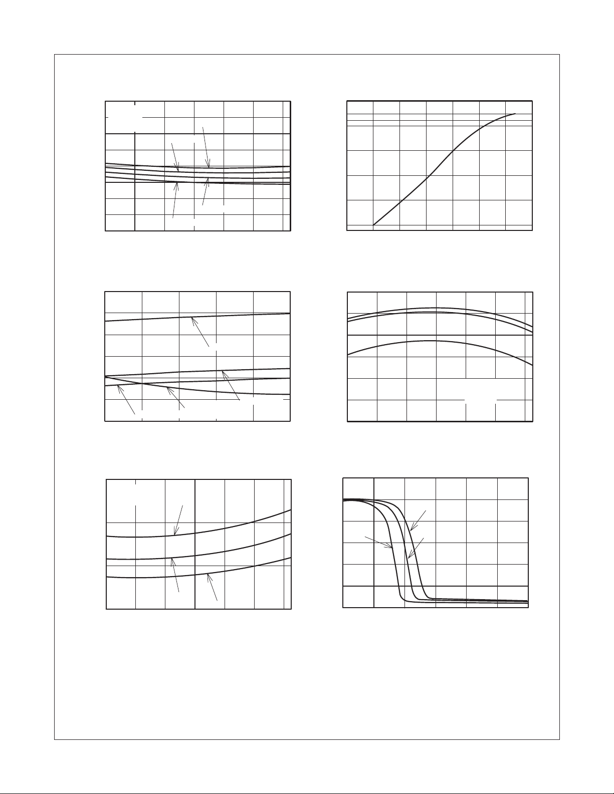
Single-channel: 6N137, HCPL-2601, HCPL-2611 Dual-Channel: HCPL-2630, HCPL-2631 High Speed-10 MBit/s Logic Gate Optocouplers
Fig.1 Low Level Output Voltage vs. Ambient Temperature
0.8
Conditions:
I
= 5 mA
F
0.7
= 2 V
V
0.6
V
E
CC
= 5.5V
I
= 12.8 mA
OL
IOL = 16 mA
0.5
utput Voltage (V)
0.4
0.3
0.2
- Low Level O
OL
0.1
V
0.0
-40 -20 0 20 40 60 80
T
- Ambient Temperature (°C)
A
IOL = 9.6 mA
IOL = 6.4 mA
Fig.3 Switching Time vs. Forward Current
120
VCC = 5 V
100
80
Delay (ns)
60
= 4 kΩ (T
R
L
Fig. 2 Input Diode Forward Voltage
vs. Forward Current
30
16
10
1
rent (mA)
0.1
- Forward Cur
0.01
F
I
0.001
0.9 1.0 1.1 1.2 1.3 1.4 1.5 1.6
VF - Forward Voltage (V)
Fig. 4 Low Level Output Current
50
45
40
)
PLH
35
vs. Ambient Temperature
I
= 15 mA
F
I
= 10 mA
F
I
= 5 mA
F
40
- Propagation
P
T
20
= 350 Ω (T
R
0
5
L
791113 15
I
RL = 1 kΩ
R
)
R
PLH
- Forward Cur
F
= 4 kΩ
L
= 350 kΩ
L
rent (mA)
(T
)
PHL
Fig. 5 Input Threshold Current
4
Conditions:
V
CC
V
O
3
Threshold Current (mA)
2
- Input
FT
I
1
-40 -20 0 20 40 60 80
vs. Ambient Temperature
= 5.0 V
= 0.6 V
RL = 350
R
L
TA - Ambient Temperature (°C)
= 1kΩ
R
= 4kΩ
L
RL = 1 kΩ (T
30
Level Output Current (mA)
25
)
PLH
- Low
OL
I
20
-40 -20 0 20 40 60 80
T
- Ambient Temperature (°C)
A
Conditions:
V
= 5 V
CC
V
= 2 V
E
V
= 0.6 V
OL
Fig. 6 Output Voltage vs. Input Forward Current
6
5
4
RL =4kΩ
3
2
- Output Voltage (V)
O
V
1
0
0123456
RL = 350Ω
RL = 1kΩ
- Forward Cur
I
F
rent (mA)
Single-channel: 6N137, HCPL-2601, HCPL-2611 Dual-Channel: HCPL-2630, HCPL-2631 Rev. 1.0.3
5 www.fairchildsemi.com
Page 6
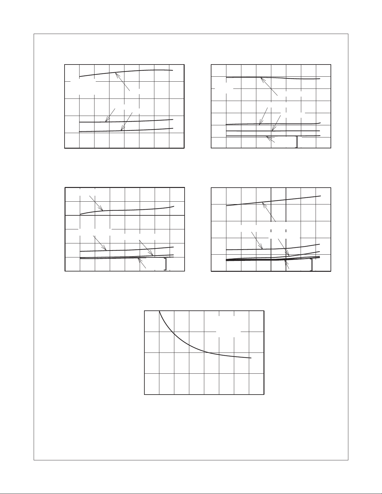
Single-channel: 6N137, HCPL-2601, HCPL-2611 Dual-Channel: HCPL-2630, HCPL-2631 High Speed-10 MBit/s Logic Gate Optocouplers
Fig. 7 Pulse Width Distortion vs. Temperature
80
60
Conditions:
I = 7.5 mA
F
V
CC = 5 V
RL = 4 kΩ
40
L = 1 kΩ
R
R
20
L = 350Ω
0
PWD - Pulse Width Distortion (ns)
-60 -40 -20 0 20 40 60 80 100
TA - Temperature (°C) TA - Temperature (°C)
Fig. 9 Enable Propagation Delay vs. Temperature
120
100
80
60
40
20
TE - Enable Propagation Delay (ns)
RL = 4 kΩ (TELH)
R
L = 1 kΩ (TELH)
0
-60 -40 -20 0 20 40 60 80 100
- Temperature (°C)
T
A
L = 350Ω (TELH)
R
RL = 350Ω
R
L = 1 kΩ
R
L = 4 kΩ
(TEHL)
Fig. 8 Rise and Fall Time vs. Temperature
600
500
Conditions:
I
F = 7.5 mA
400
V
CC = 5 V
300
200
RL = 1 kΩ (tr)
R
LR = 4 kΩ (tr)
L = 350Ω (tr)
100
Tr/Tf - Rise and Fall Time (ns)
0
L = 1 kΩ
R
R
L = 4 kΩ (tf)
R
L = 350Ω
-60 -40 -20 0 20 40 60 80 100
Fig. 10 Switching Time vs. Temperature
120
100
80
RL = 1 kΩ TPLH
60
Propagation Delay (ns)
40
TP -
20
-60 -40 -20 0 20 40 60 80 100
T
RL = 4 kΩ TPLH
RL = 350Ω TPLH
- Temperature (°C)
A
RL = 1 kΩ
RL = 4 kΩ
RL = 350Ω
TPHL
Fig. 11 High Level Output Current
vs. Temperature
20
Conditions:
VCC = 5.5 V
V
= 5.5 V
O
V
= 2.0 V
15
E
I
= 250 µA
F
10
5
IOH - High Level Output Current (µA)
0
-60 -40 -20 0 20 40 60 80 100
- Temperature (°C)
T
A
6 www.fairchildsemi.com
Single-channel: 6N137, HCPL-2601, HCPL-2611 Dual-Channel: HCPL-2630, HCPL-2631 Rev. 1.0.3
Page 7
Input
Monitor
(I )
F
Pulse
Generator
tr = 5ns
Z = 50Ω
O
47
V
1
CC
2
3
4 5
GND
Single-channel: 6N137, HCPL-2601, HCPL-2611 Dual-Channel: HCPL-2630, HCPL-2631 High Speed-10 MBit/s Logic Gate Optocouplers
+5V
I = 7.5 mA
F
PLH
I = 3.75 mA
F
1.5 V
t
r
8
.1 µf
7
bypass
6
R
L
Output
(V )
O
C
L
Input
(I )
F
Output
(V )
O
Output
(V )
O
t
PHL
t
f
t
90%
10%
Pulse
Generator
tr = 5ns
Z = 50Ω
O
7.5 mA
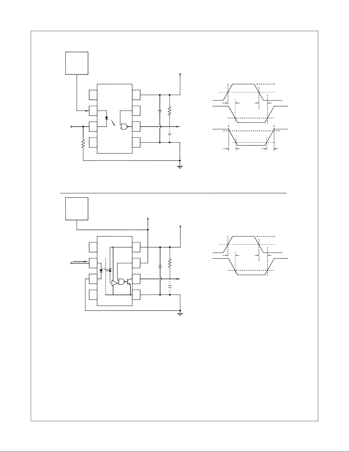
Fig. 12 Test Circuit and Waveforms for t
Input
Monitor
(V )
E
+5V
and t
Input
(V )
E
Output
(V )
O
ELH
V
1
2
3
4
CC
8
7
.1 µf
bypass
R
L
6
C
L
5
GND
Fig. 13 Test Circuit t
Output
(V )
O
EHL
, t
PLH
PHL, tr
tt
EHL
and tf.
3.0 V
1.5 V
ELH
1.5 V
.
Single-channel: 6N137, HCPL-2601, HCPL-2611 Dual-Channel: HCPL-2630, HCPL-2631 Rev. 1.0.3
7 www.fairchildsemi.com
Page 8
Single-channel: 6N137, HCPL-2601, HCPL-2611 Dual-Channel: HCPL-2630, HCPL-2631 High Speed-10 MBit/s Logic Gate Optocouplers
V
CC
1
I
A
B
V
FF
F
2
3
8
7
6
.1 µf
bypass
350Ω
+5V
Output
(V )
O
V
CM
0V
5V
V
O
V
O
0.5 V
4
Pulse Gen
Switching Pos. (A), I = 0
V (Min)
O
Switching Pos. (B), I = 7.5 mA
Peak
GND
V
CM
F
V (Max)
O
5
CM
H
F
CM
L
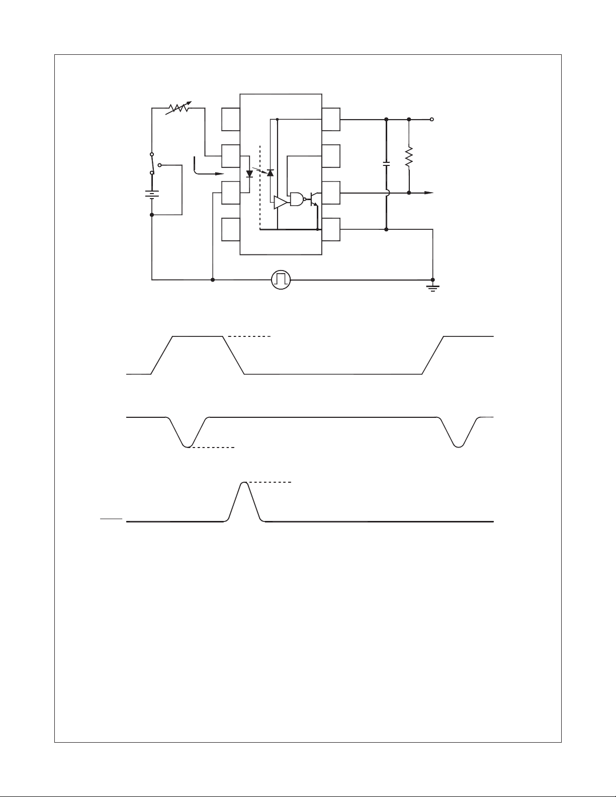
Fig. 14 Test Circuit Common Mode Transient Immunity
Single-channel: 6N137, HCPL-2601, HCPL-2611 Dual-Channel: HCPL-2630, HCPL-2631 Rev. 1.0.3
8 www.fairchildsemi.com
Page 9
Single-channel: 6N137, HCPL-2601, HCPL-2611 Dual-Channel: HCPL-2630, HCPL-2631 High Speed-10 MBit/s Logic Gate Optocouplers
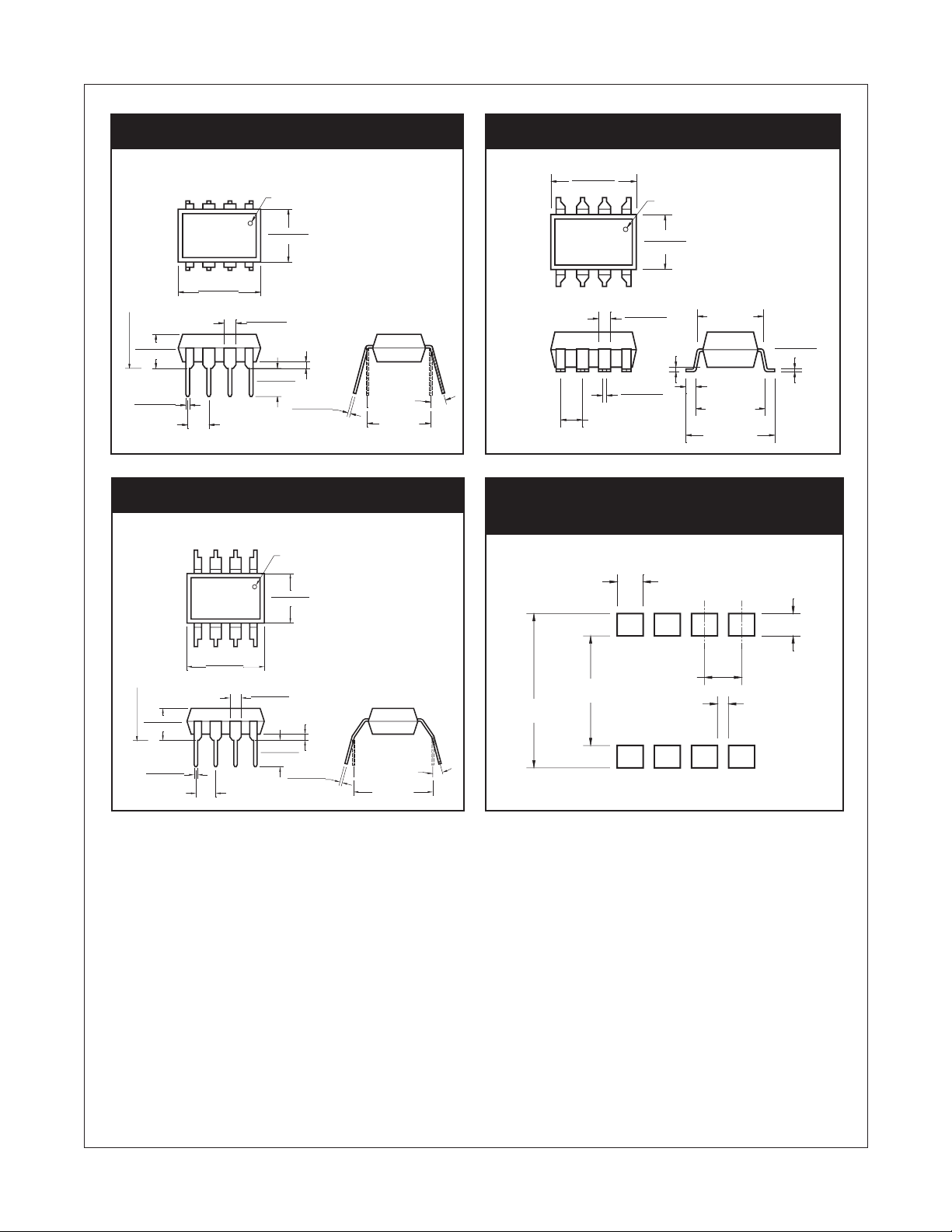
Package Dimensions (Through Hole)
PIN 1
ID.
241
0.270 (6.86)
0.250 (6.35)
8
0.070 (1.78)
0.045 (1.14)
0.020 (0.51) MIN
0.154 (3.90)
0.120 (3.05)
0.016 (0.40)
0.008 (0.20)
15° MAX
0.300 (7.62)
TYP
0.200 (5.08)
0.140 (3.55)
SEATING PLANE
0.022 (0.56)
0.016 (0.41)
3
56 7
0.390 (9.91)
0.370 (9.40)
0.100 (2.54) TYP
Package Dimensions (0.4"Lead Spacing)
PIN 1
3
56 78
ID.
241
0.270 (6.86)
0.250 (6.35)
Package Dimensions (Surface Mount)
0.390 (9.91)
0.370 (9.40)
3214
567
0.100 (2.54)
Lead Coplanarity : 0.004 (0.10) MAX
TYP
0.270 (6.86)
0.250 (6.35)
8
0.070 (1.78)
0.045 (1.14)
0.022 (0.56)
0.016 (0.41)
PIN 1
ID.
0.020 (0.51)
MIN
0.300 (7.62)
TYP
0.045 [1.14]
0.315 (8.00)
MIN
0.405 (10.30)
MIN
0.016 (0.41)
0.008 (0.20)
Recommended Pad Layout for
Surface Mount Leadform
0.070 (1.78)
0.060 (1.52)
0.390 (9.91)
0.370 (9.40)
0.070 (1.78)
0.045 (1.14)
0.200 (5.08)
0.140 (3.55)
SEATING PLANE
0.022 (0.56)
0.016 (0.41)
0.100 (2.54) TYP
0.004 (0.10) MIN
0.154 (3.90)
0.120 (3.05)
0.016 (0.40)
0.008 (0.20)
NOTE
All dimensions are in inches (millimeters)
0° to 15°
0.400 (10.16)
TYP
0.415 (10.54)
0.295 (7.49)
0.100 (2.54)
0.030 (0.76)
Single-channel: 6N137, HCPL-2601, HCPL-2611 Dual-Channel: HCPL-2630, HCPL-2631 Rev. 1.0.3
9 www.fairchildsemi.com
Page 10
Ordering Information
Option Example Part Number Description
S 6N137S Surface Mount Lead Bend
SD 6N137SD Surface Mount; Tape and reel
W 6N137W 0.4" Lead Spacing
V 6N137V VDE0884
TV 6N137TV VDE0884; 0.4” lead spacing
SV 6N137SV VDE0884; surface mount
SDV 6N137SDV VDE0884; surface mount; tape and reel
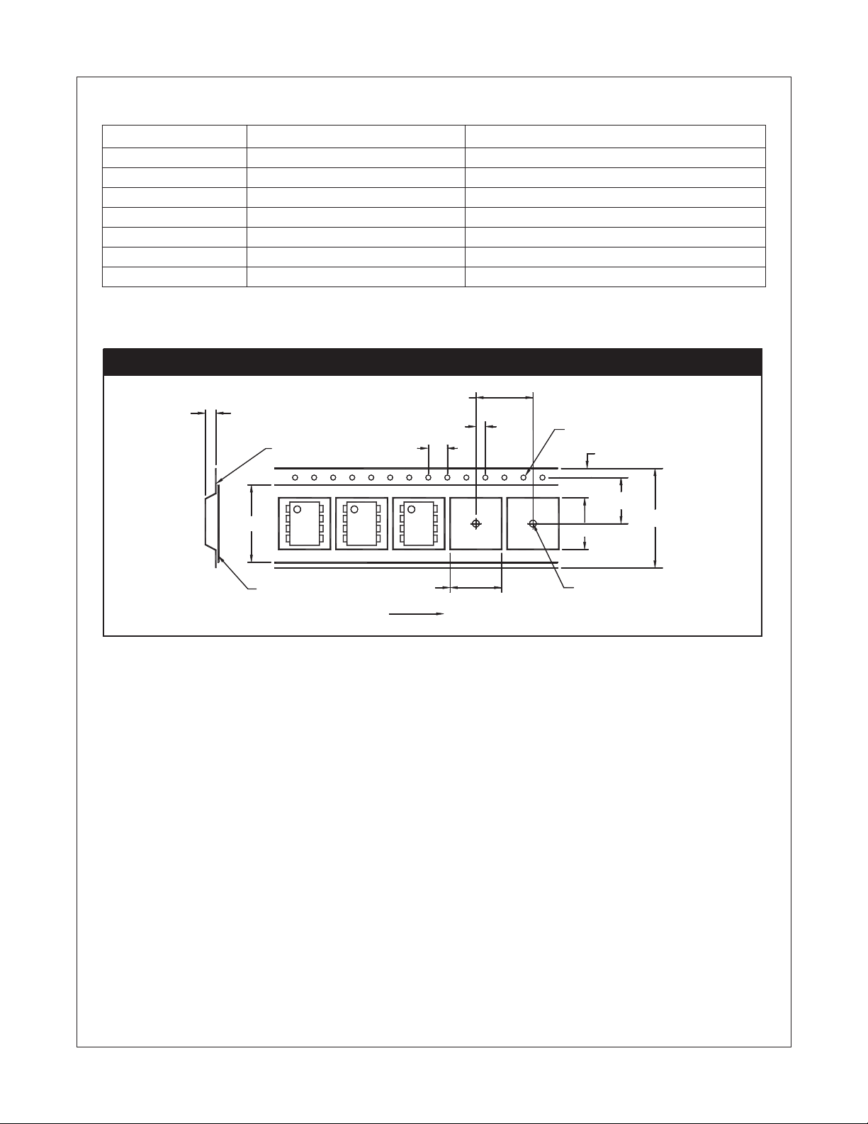
QT Carrier Tape Specifications (“D” Taping Orientation)
12.0 ± 0.1
4.90 ± 0.20
0.30 ± 0.05
4.0 ± 0.1
4.0 ± 0.1
Single-channel: 6N137, HCPL-2601, HCPL-2611 Dual-Channel: HCPL-2630, HCPL-2631 High Speed-10 MBit/s Logic Gate Optocouplers
Ø1.55 ± 0.05
1.75 ± 0.10
13.2 ± 0.2
0.1 MAX
User Direction of Feed
10.30 ± 0.20
7.5 ± 0.1
16.0 ± 0.3
10.30 ± 0.20
Ø1.6 ± 0.1
Single-channel: 6N137, HCPL-2601, HCPL-2611 Dual-Channel: HCPL-2630, HCPL-2631 Rev. 1.0.3
10 www.fairchildsemi.com
Page 11
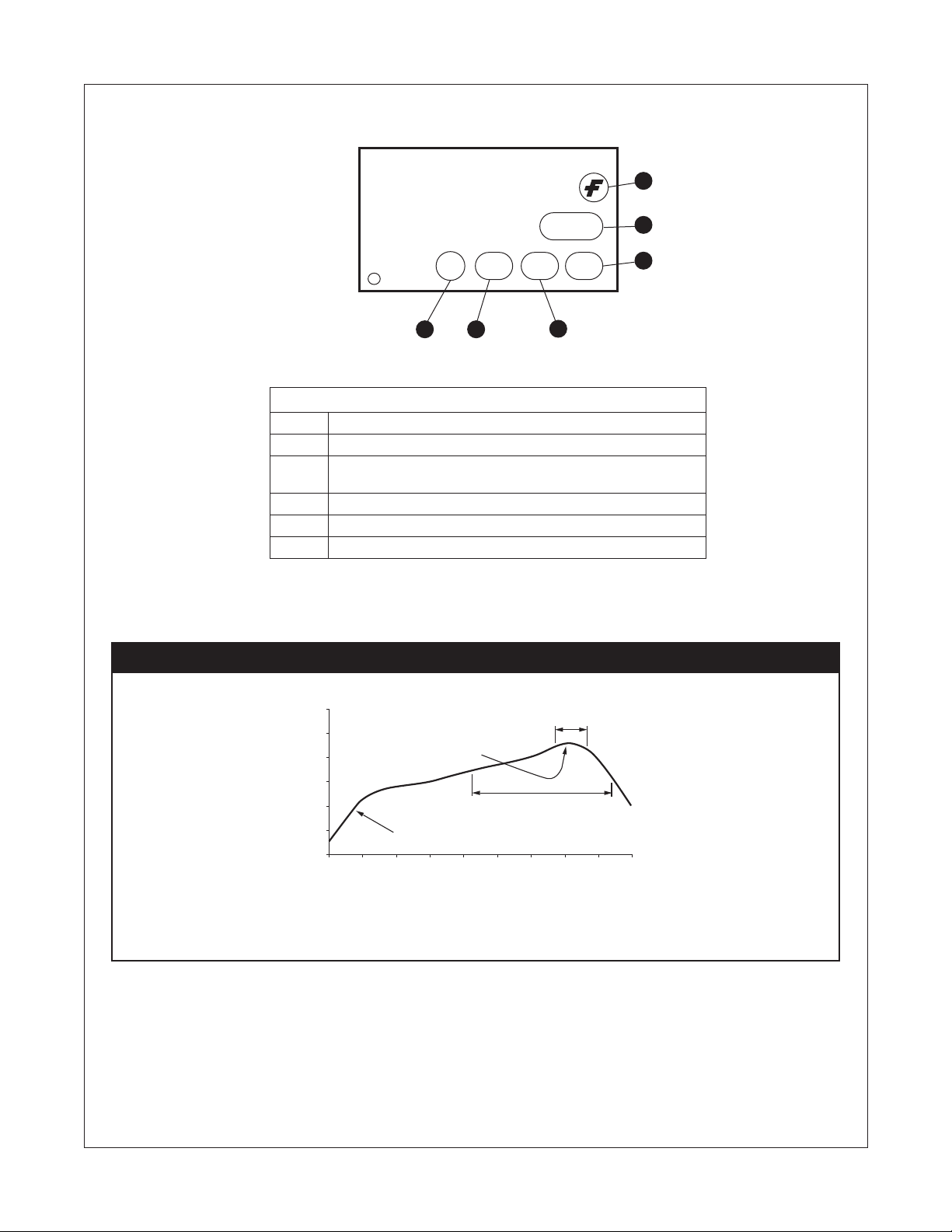
Marking Information
Single-channel: 6N137, HCPL-2601, HCPL-2611 Dual-Channel: HCPL-2630, HCPL-2631 High Speed-10 MBit/s Logic Gate Optocouplers
1
Reflow Profile
2601
T1YYXXV
43
5
2
6
Definitions
1Fairchild logo
2Device number
3 VDE mark (Note: Only appears on parts ordered with VDE option –
See order entry table)
4Two digit year code, e.g., ‘03’
5Two digit work week ranging from ‘01’ to ‘53’
6 Assembly package code
300
250
Temperature (°C)
200
150
100
50
0
0.5 1 1.5 2 2.5 3 3.5 4 4.5
0
• Peak reflow temperature: 225 C (package surface temperature)
• Time of temperature higher than 183 C for 60–150 seconds
• One time soldering reflow is recommended
225 C peak
Ramp up = 3
Time (Minute)
Time above 183 C, 60–150 sec
C/sec
215 C, 10–30 s
Single-channel: 6N137, HCPL-2601, HCPL-2611 Dual-Channel: HCPL-2630, HCPL-2631 Rev. 1.0.3
11 www.fairchildsemi.com
Page 12
TRADEMARKS
The following are registered and unregistered trademarks Fairchild Semiconductor owns or is authorized to use and is
not intended to be an exhaustive list of all such trademarks.
ACEx™
ActiveArray™
Bottomless™
FPS™
Build it Now™
CoolFET™
CROSSVOLT™
DOME™
EcoSPARK™
2
E
CMOS™
EnSigna™
FACT™
FACT Quiet Series™
Across the board. Around the world.™
The Power Franchise
Programmable Active Droop™
DISCLAIMER
FAIRCHILD SEMICONDUCTOR RESERVES THE RIGHT TO MAKE CHANGES WITHOUT FURTHER NOTICE TO ANY
PRODUCTS HEREIN TO IMPROVE RELIABILITY, FUNCTION OR DESIGN. FAIRCHILD DOES NOT ASSUME ANY LIABILITY
ARISING OUT OF THE APPLICATION OR USE OF ANY PRODUCT OR CIRCUIT DESCRIBED HEREIN; NEITHER DOES IT
CONVEY ANY LICENSE UNDER ITS PATENT RIGHTS, NOR THE RIGHTS OF OTHERS.
LIFE SUPPORT POLICY
FAST
FASTr™
LittleFET™
FRFET™
GlobalOptoisolator™
GTO™
HiSeC™
2
I
C™
i-Lo™
ImpliedDisconnect™
IntelliMAX™
ISOPLANAR™
MICROCOUPLER™
MicroFET™
MicroPak™
MICROWIRE™
MSX™
MSXPro™
OCX™
OCXPro™
OPTOLOGIC
OPTOPLANAR™
PACMAN™
POP™
Power247™
PowerEdge™
PowerSaver™
PowerTrench
QFET
QS™
QT Optoelectronics™
Quiet Series™
RapidConfigure™
RapidConnect™
µSerDes™
SILENT SWITCHER
SMART START™
SPM™
Stealth™
SuperFET™
SuperSOT™-3
SuperSOT™-6
SuperSOT™-8
SyncFET™
TinyLogic
TINYOPTO™
TruTranslation™
UHC™
UltraFET
UniFET™
VCX™
Wire™
Single-channel: 6N137, HCPL-2601, HCPL-2611 Dual-Channel: HCPL-2630, HCPL-2631 High Speed-10 MBit/s Logic Gate Optocouplers
FAIRCHILD’S PRODUCTS ARE NOT AUTHORIZED FOR USE AS CRITICAL COMPONENTS IN LIFE SUPPORT
DEVICES OR SYSTEMS WITHOUT THE EXPRESS WRITTEN APPROVAL OF FAIRCHILD SEMICONDUCTOR CORPORATION.
As used herein:
1. Life support devices or systems are devices or
systems which, (a) are intended for surgical implant into
the body, or (b) support or sustain life, or (c) whose
failure to perform when properly used in accordance
with instructions for use provided in the labeling, can be
reasonably expected to result in significant injury to the
user.
PRODUCT STATUS DEFINITIONS
Definition of Terms
Datasheet Identification Product Status Definition
Advance Information
Preliminary
No Identification Needed
Formative or
In Design
First Production
Full Production
2. A critical component is any component of a life
support device or system whose failure to perform can
be reasonably expected to cause the failure of the life
support device or system, or to affect its safety or
effectiveness.
This datasheet contains the design specifications for
product development. Specifications may change in
any manner without notice.
This datasheet contains preliminary data, and
supplementary data will be published at a later date.
Fairchild Semiconductor reserves the right to make
changes at any time without notice in order to improve
design.
This datasheet contains final specifications. Fairchild
Semiconductor reserves the right to make changes at
any time without notice in order to improve design.
Obsolete
Single-channel: 6N137, HCPL-2601, HCPL-2611 Dual-Channel: HCPL-2630, HCPL-2631 Rev. 1.0.3
Not In Production
This datasheet contains specifications on a product
that has been discontinued by Fairchild semiconductor.
The datasheet is printed for reference information only.
12 www.fairchildsemi.com
Rev. I16
 Loading...