

LITEON 1N5822, 1N5820, 1N5821 Datasheet
LITE-ON
SEMICONDUCTOR
1N5820 thru 1N5822
SCHOTTKY BARRIER RECTIFIERS
FEATURES
Metal-Semiconductor junction with guard ring
Epitaxial construction
Low forward voltage drop
High current capability
The plastic material carries UL recognition 94V-0
For use in low voltage,high frequency inverters,free
wheeling,and polarity protection applications
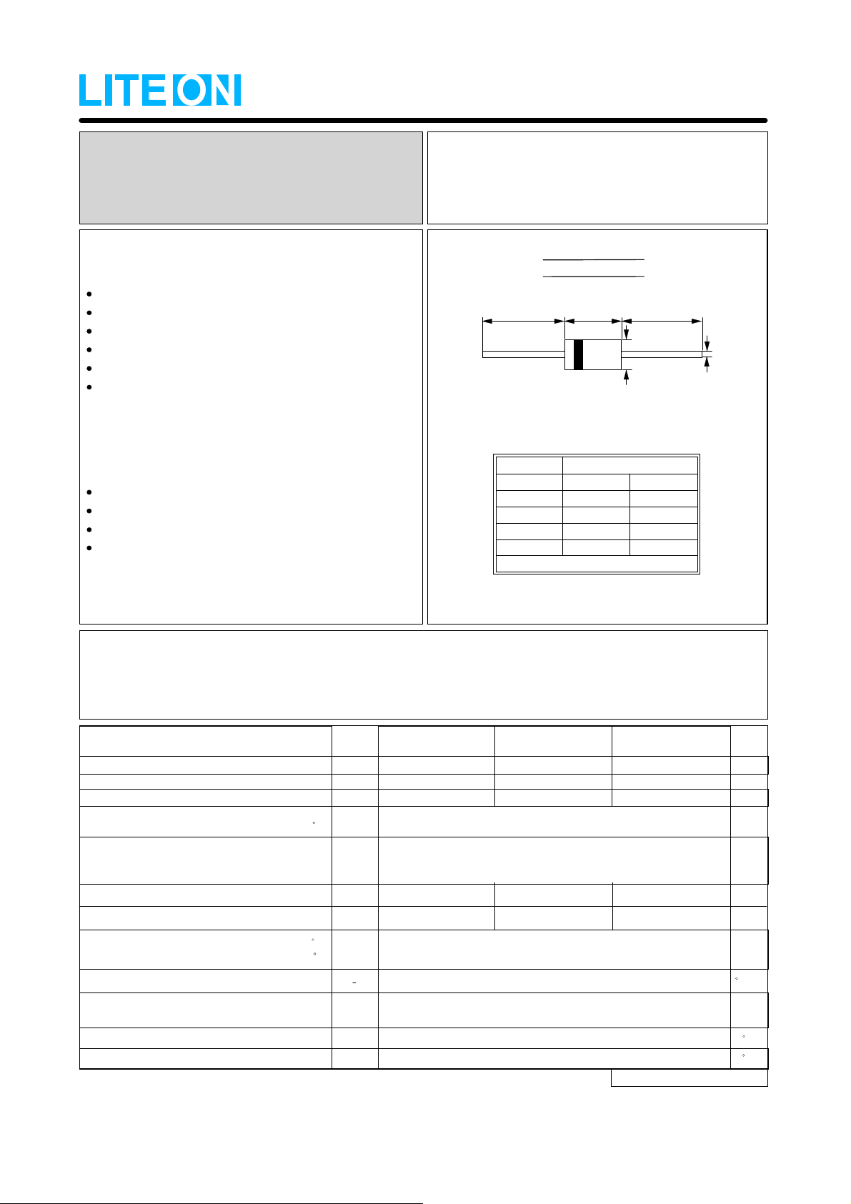
MECHANI CAL DATA
Case : JEDEC DO-201AD molded plastic
Polarity : Color band denotes cathode
Weight : 0.04 ounces, 1.1 grams
Mounting position : Any
REVERSE VOLTAGE
FORWARD CURRENT
DO-201AD
A
Dim.
A
B
C
D
All Dimensions in millimeter
B
DO-201AD
Min.
25.4
7.30
1.20
4.80 5.30
- 20 to 40
- 3.0
Amperes
A
D
Max.
-
9.50
1.30
Volts
C
MAXIMUM RATINGS AND ELECTRICAL CHARACTERISTICS
Ratings at 25℃ ambient temperature unless otherwise specified.
Single phase, half wave, 60Hz, resistive or inductive load.
For capacitive load, der a te current by 20%
1N5820
20
14
20
0.475
=
95 C
SYMBOL
RRM
V
RMS
V
DC
V
(AV)
I
FSM
I
F
V
F
V
R
I
R
0JL
J
C
J
T
STG
T
CHARACTERISTICS
Maximum Recurren t Peak Reverse Volt age
Maximum RMS Voltage
Maximum DC Blocking Voltage
Maximum Average Forward Rectified Current
.375",(9.5mm) Lead Lengths
Peak Forward Surge Current
8.3ms single half sine-wave
super imposed on rated load
Maximum forward V oltage a t 3.0A DC
Maximum forward V oltage a t 9.4A DC
Maximum DC Reverse Current
at Rated DC Blocking Voltage
Typical Thermal Resistance (Note 1)
Typical Junction
Capacitance (Note 2)
Operating Temperature Range
Storage Temperature Range
NOTES : 1.Thermal Resistance Junction to Lead.
2.Measured at 1.0MHz and applied reverse voltage of 4.0V DC.
@T
L
@TJ =25 C
@TJ =100 C
1N5821
30
21
30
3.0
80
0.500
0.9000.850
2
20
20
250
-55 to +125
-55 to +150 C
1N5822
40
28
40
0.525
0.950
REV. 2, 01-Dec-2000, KDHF01
UNIT
V
V
V
A
A
V
V
mA
mA
C/W
pF
C
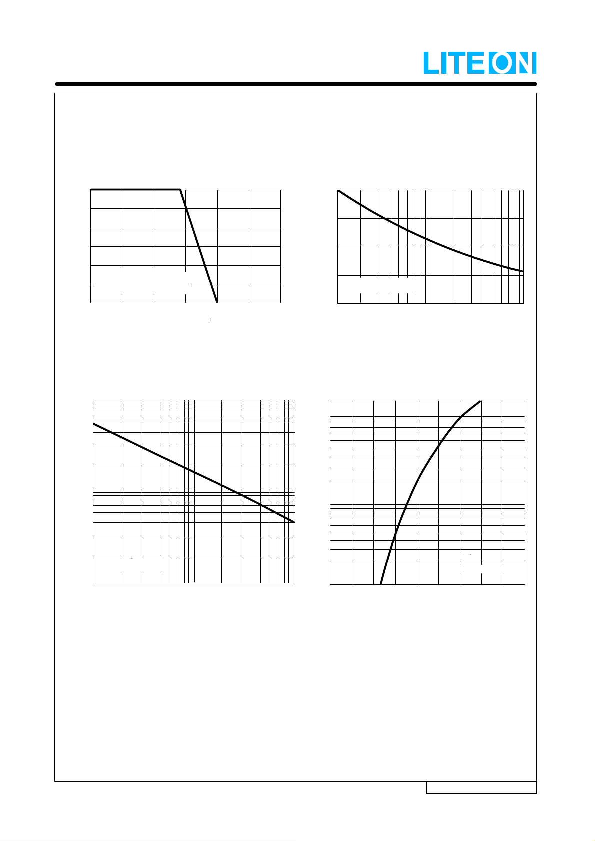
RATING AND CHARACTERISTIC CURVES
1N5820 thru 1N5822
FIG.1 - FORWARD CURRENT DERATING CURVE
3.0
2.0
1.0
SINGLE PHASE HALF WAVE 60Hz
RESISTI V E OR INDUCT I VE LOAD
0.375" (9.5mm) LEAD LENGTHS
AVERAGE FORWARD CURRENT
AMPERES
0
25
50
75 100 125 150
LEAD TEMPERATURE , C
FIG.3 - TYPICAL JUNCTION CAPACITANCE
1000
175
FIG.2 - MAXIMUM NON-REPETITIVE SURGE CURRENT
80
60
40
20
Single Half-Sine-Wave
(JEDEC METHOD)
0
PEAK FO RWA RD SURGE CURRENT,
AMPERES
1 5 10 50 1002
20
NUMBER OF CYCLES AT 60Hz
FIG.4 - TYPICAL FORWARD CHARACTERISTICS
20
10
100
1.0
CAPACITANCE , (p F)
TJ= 25 C, f= 1MHz
10
1
10
104
REVERSE VOLTAGE , VOLTS
100
INSTANTANEOUS FORWARD CURRENT ,(A)
0.1
0.3
0.2
0.1
0
0.4 0.5 0.6
INSTANTANEOUS FORWARD VOLTAGE , VOLTS
TJ= 25 C
PULSE WIDTH 300us
PULSE WIDTH 300us
0.8
0.7
0.9
REV. 2, 01-Dec-2000, KDHF01
 Loading...