

Page 1

Global LCD Panel Exchange Center
LITEMAX LF1745
www.panelook.com
Sunlight Readable 17" LCD Display
(1st Edition 4/9/2004 )
All information is subject to change without notice.
LITEMAX Electronics Inc.
4F, No.131-3, Lane235, Bau-chiau Rd.,
Shin-dian City, Taipei County, Taiwan R.O.C.
Tel : 886-2-8919-1858
Fax: 886-2-8919-1300
Homepage: http://www.litemax.com.tw
One step solution for LCD / PDP / OLED panel application: Datasheet, inventory and accessory!
www.panelook.com
Page 2

Global LCD Panel Exchange Center
Contents
Introduction and Overview...3
General Specifications...4
Functional Block Diagram
Optical Characteristics
Pixel format image.
Electrical characteristics...9
Absolute Maximum Ratings
Connectors
www.panelook.com
Signal Pin
Signal Description
Signal Electrical Characteristics
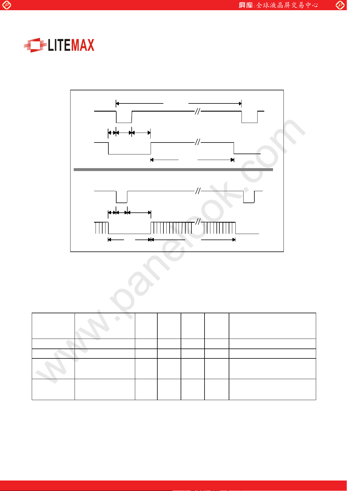
Interface Timing
Timing Characteristics
Timing Definition
Power Consumption
Power ON/OFF Sequence
Backlight Characteristics...17
Signal for Lamp connector
Reliability and Lifetime...18
Mechanical Characteristics...19
Litemax LI3601 Inverter...20
LF1745 Page 2
One step solution for LCD / PDP / OLED panel application: Datasheet, inventory and accessory!
www.panelook.com
Page 3

Global LCD Panel Exchange Center
INTRODUCTION AND OVERVIEW
This is a product specification that specifies form, fit, and function of the 17” TFT LCD monitor and its
options. The LF1745 products are a family of high bright LCD monitors intended for use in a variety of
industrial and commercial applications. Some of these applications include automatic teller machines (ATMs),
fuel dispensing systems, ticketing and information kiosks, and intelligent vending machines. The LCD panel for
LF1745 has a particularly fast response time of 16ms and consequently very well suited for video applications.
The LF1745 is a 17” active matrix TFT LCD with a native resolution of 1280X1024. It has a typical
luminance of 1000 nits with a +12VDC input. The video interface is through a standard 15 pin analog input with
an integrated On-Screen Display (OSD).
OUTLINE
STRUCTURE AND PRINCIPLE
LF1745 module is composed of the driver LSIs for driving the TFT (Thin Film Transistor) array with an
amorphous silicon thin film transistor liquid crystal display (a-Si TFT LCD) panel structure and a backlight.
The a-Si TFT LCD panel structure is injected liquid crystal material into the narrow gap between a TFT array
glass substrate and a color filter glass substrate.
RGB (Red, Green, and Blue) data signals from a source system are modulated into a form suitable for active
matrix addressing by the onboard signal processor and sent to the driver LSIs which in turn address the
individual TFT cells.
Working as an electro-optical switch, each TFT cell regulates transmitted light from the backlight assembly
when worked by the data source. Color images are created by regulating the amount of transmitted light through
the array of red, green and blue dots.
www.panelook.com
APPLICATIONS
ΘKiosk, Public, Health Application, LCD TV, POI, Ticketing, Advertising, Gaming, Industrial Computing, Signage...
FEATURES
Θwide viewing angle
ΘFast response time
ΘHigh luminance
ΘHigh contrast
ΘWide color gamut
ΘLuminance control
ΘSmall foot prints
LF1745 Page 3
One step solution for LCD / PDP / OLED panel application: Datasheet, inventory and accessory!
www.panelook.com
Page 4
Global LCD Panel Exchange Center
GENERAL SPECIFICATIONS
Display area 337.92 (H) x 270.336 (V) mm
Drive system a-Si TFT active matrix
Display colors 262k
Number of pixels 1280 (H) x 1024 (V) pixel
Pixel arrangement RGB (Red, Green, Blue) vertical stripe
Pixel pitch 0.264 (H) x 0.264 (V) mm
Module size 358.5(H) x 296.5 (V) x 29(D) mm
Weight 1670 g (typ.)
Contrast ratio 500:1 (typ.)
Viewing angle At the contrast ratio 10:1
www.panelook.com
ΘHorizontal: Left side 80° (typ.), Right side 80° (typ.)
ΘVertical: Up side 75° (typ.), Down side 75° (typ.)
Designed viewing direction
Polarizer pencil-hardness 3H (min.) [by JIS K5400]
Color gamut At LCD panel center
Response time 16 ms (typ.)
Luminance 1000 cd/m
Backlight
Power consumption At maximum luminance and checkered flag pattern
ΘOptimum grayscale (ӫ=2.2): perpendicular
60% (typ.) [against NTSC color space]
Ton (black 10% white 90%)
ΘBacklight unit: AU 1745
ΘInverter: LI3601
55 W (typ.)
2
(typ.)
Ш
LF1745 Page 4
One step solution for LCD / PDP / OLED panel application: Datasheet, inventory and accessory!
www.panelook.com
Page 5
Global LCD Panel Exchange Center
www.panelook.com
Functional Block Diagram
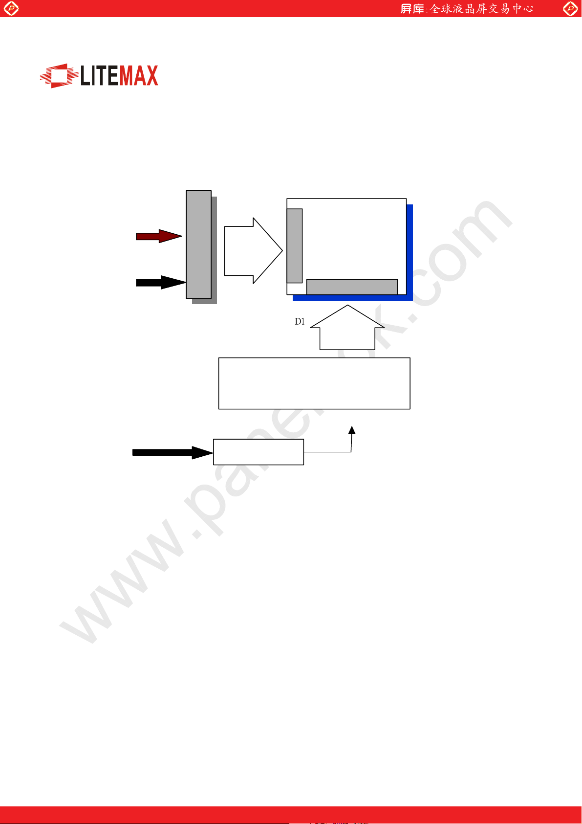
The following diagram shows the functional block of the 17.0 inches Color TFT-LCD Module:
G1
LVDS
Con n ector
Y-Driver IC
TFT-LCD
1280*(3) *1024
+ 5 V
G1024
Pixels
X-Driver IC
DC P OWE R
D3840
10 CCFL
Inverter
LF1745 Page 5
One step solution for LCD / PDP / OLED panel application: Datasheet, inventory and accessory!
www.panelook.com
Page 6
Global LCD Panel Exchange Center
Optical Characteristics
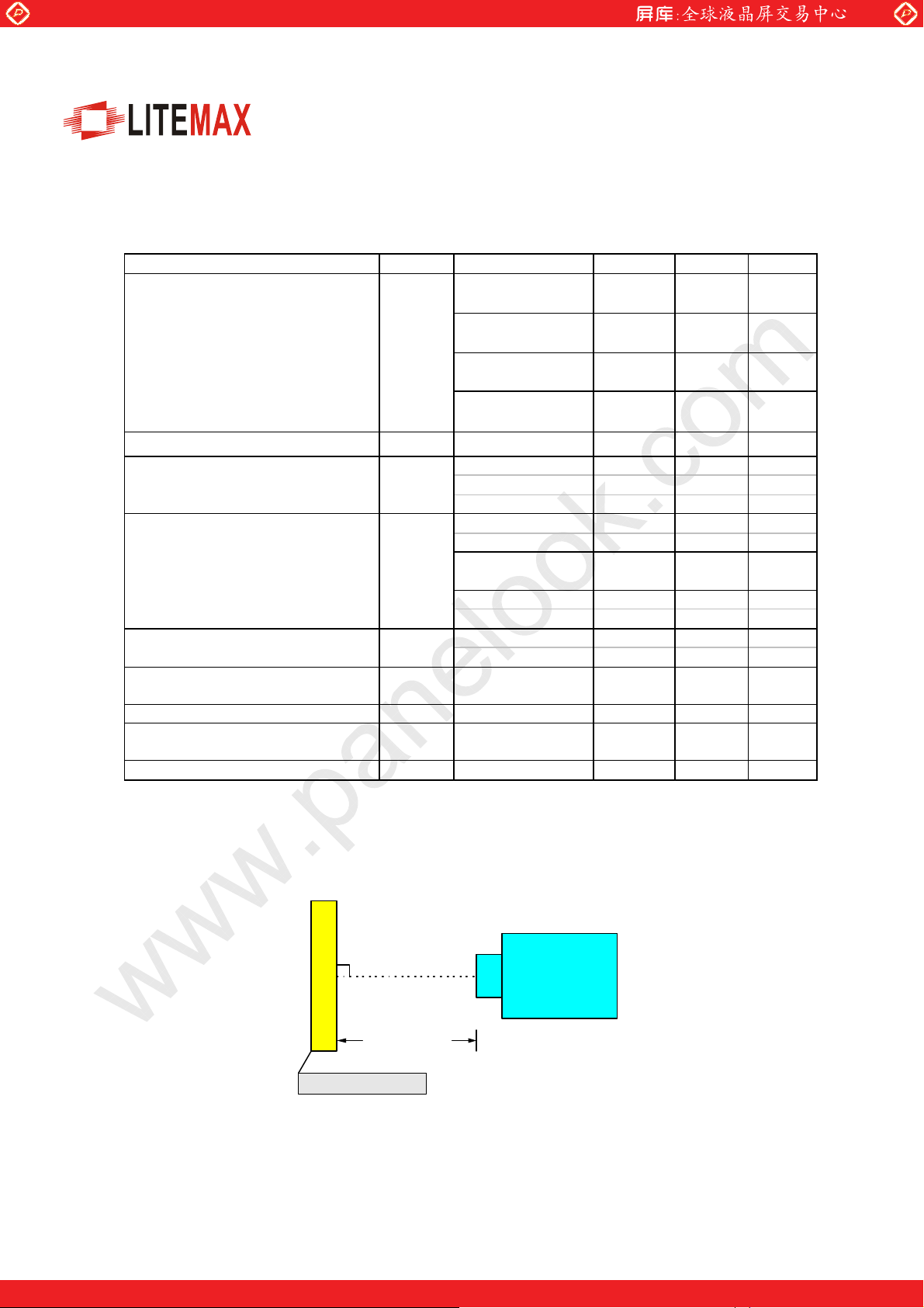
The optical characteristics are measured under stable conditions at 25℃ (Room Temperature) :
Item Unit Conditions Min. Typ. Max.
Viewing Angle [degree]
Contrast ratio Normal Direction - -
Response Time (Note 1) [msec]
Color / Chromaticity
Coordinates (CIE)
Color Coordinates (CIE) White
White Luminance @ CCFL 7.0mA
(center)
Luminance Uniformity (Note 2) [%] 75 80 TCO99 1.5.2B luminance uniformity
(Note 3)
Crosstalk (in 75Hz) (Note 4) [% ] 1.5
www.panelook.com
Horizontal (Right)
CR = 10 (Left)
Vertical (Up)
CR = 10 (Down)
Horizontal (Right)
CR = 5 (Left)
Vertical (Up)
CR = 5 (Down)
Raising Time - 4 5
Falling Time - 12 20
Raising + Falling - 16 25
Red x 0.61 0.64 0.67
Red y 0.31 0.34 0.37
Green x 0.26 0.29 0.32
Green y 0.58 0.61 0.64
Blue x 0.11 0.14 0.17
Blue y 0.04 0.07 0.10
White x 0.28 0.31 0.34
White y 0.30 0.33 0.36
[cd/m2]
- -
60
60
60
60
70
70
70
70
80
80
75
75
85
85
80
80
500
1000
-
-
-
-
-
-
1.7
Equipment Pattern Generator, Power Supply, Digital Voltmeter, Luminance meter (PR 880, BM-5A)
Aperture 1°with 100cm VD or 2°with 50cm viewing distance
Test Point Center (ISO point 22)
Environment < 1 lux
LCD Module
PR-880 /
BM5A /
BM7
measuring distance
Module Driving Equipment
LF1745 Page 6
One step solution for LCD / PDP / OLED panel application: Datasheet, inventory and accessory!
www.panelook.com
Page 7
Global LCD Panel Exchange Center
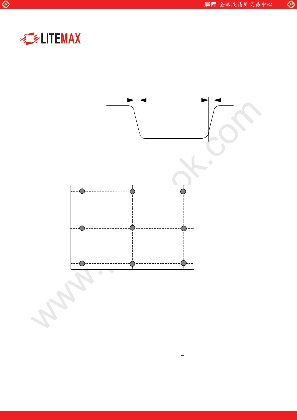
Note 1: Definition of Response time:
The output signals of photodetector are measured when the input signals are changed from “ Black” to “ White”
(falling time), and from “ White” to “ Black” (rising time), respectively. The response time is interval between the 10%
and 90% of amplitudes.
%
100
90
Optical
Response
www.panelook.com
TrR
TrD
10
Note 2: Brightness uniformity of these 9 points is defined as below:
90 %
white
0
50 %
white
black
10 %
10 %
50 %
90 %
Minimum Luminance in 9 Points (1-9)
Uniformity = ————————————————————
Maximum Luminance in 9 Points (1-9)
Note 3: TCO ’ 99 Certification Requirements and test methods for environmental labeling of Display Report No. 2
defines Luminance uniformity as below:
((Lmax,+30deg. / Lmin,+30deg.) + (Lmax,-30deg. / Lmin,-30deg.)) / 2
This panel is compatible with TCO99 approbation in luminance uniformity <
1.7, luminance contrast >0.5
LF1745 Page 7
One step solution for LCD / PDP / OLED panel application: Datasheet, inventory and accessory!
www.panelook.com
Page 8
Global LCD Panel Exchange Center
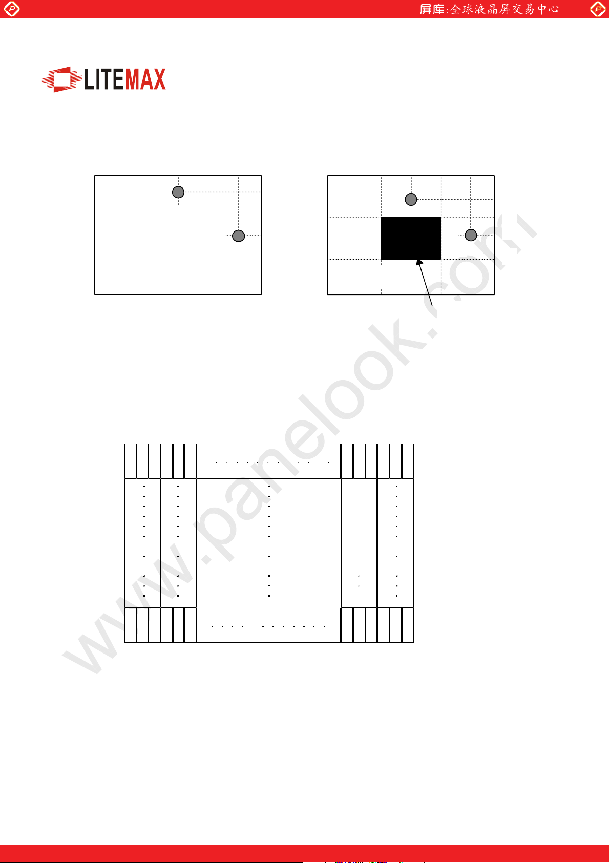
Note 4:
www.panelook.com
1/2
A
184 gray level 184 gray level
Unit: percentage of dimension of display area
l L
l L
l / LA x 100%= 1.5% max., LA and LB are brightness at location A and B
A-LA’
l / LB x 100%= 1.5% max., LA’ and LB’ are brightness at location A’ and B’
B-LB’
1/6
1/6
1/2
B
2/3 1/3
A’
Pixel format image
Following figure shows the relationship of the input signals and LCD pixel format.
1 2 1279 1280
1/2
1/6
1/6
1/3
1/2
B’
2/3
0 gray level
1st Line
1024th
R G B R G B
R G B R G B
R G B R G B
R G B R G B
LF1745 Page 8
One step solution for LCD / PDP / OLED panel application: Datasheet, inventory and accessory!
www.panelook.com
Page 9
Global LCD Panel Exchange Center
emperature
C
Electrical characteristics
Absolute Maximum Ratings
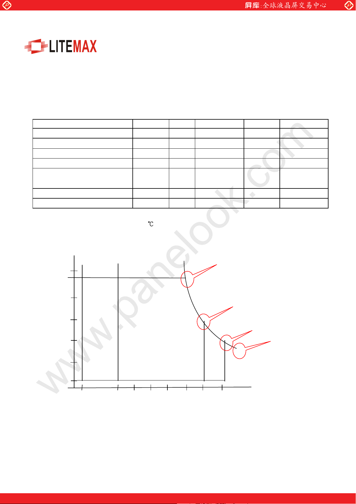
Absolute maximum ratings of the module is as following:
Item Symbol Min Ma x Unit Conditions
Logic/LCD Drive Voltage VIN -0.3 +5.5 [Volt]
Select LVDS data order SELLVDS NC NC [Volt]
CCFL Inrush current ICFLL - 38 [mA]
CCFL Current ICFL - 7.6 [mA] rms
Operating Temperature TOP 0 +50 [oC] Note 1
Operating Humidity HOP 8 95 [%RH] Note 1
www.panelook.com
Storage Temperature TST -20 +60 [oC] Note 1
Storage Humidity HST 8 95 [%RH] Note 1
Note 1 : Maximum Wet-Bulb should be 39Ċ and No condensation.
Relative Humidity %
100
95
80
60
40
20
Storage
range
Twb=39
Operation range
℃
T=40℃,H=95%
T=50℃,H=55%
T=60℃,H=39%
T=65℃,H=29%
Storage
range
5
0
-20
LF1745 Page 9
One step solution for LCD / PDP / OLED panel application: Datasheet, inventory and accessory!
06050
T
o
www.panelook.com
Page 10
Global LCD Panel Exchange Center
www.panelook.com
Connectors
Physical interface is described as for the connector on module.
These connectors are capable of accommodating the following signals and will be following components.
Connector Name / Designation Interface Connector / Interface card
Manufacturer JAE or compatible
Type Part Number F I-X30S -HF
Mating Housing Part Number FI- X30S -H
Connector Name / Designation Lamp Connector / Backlight lamp
Manufacturer JST
Type Part Number BHR-04VS-1
Mating Type Part Number SM04(4.0)B-BHS-1-TB
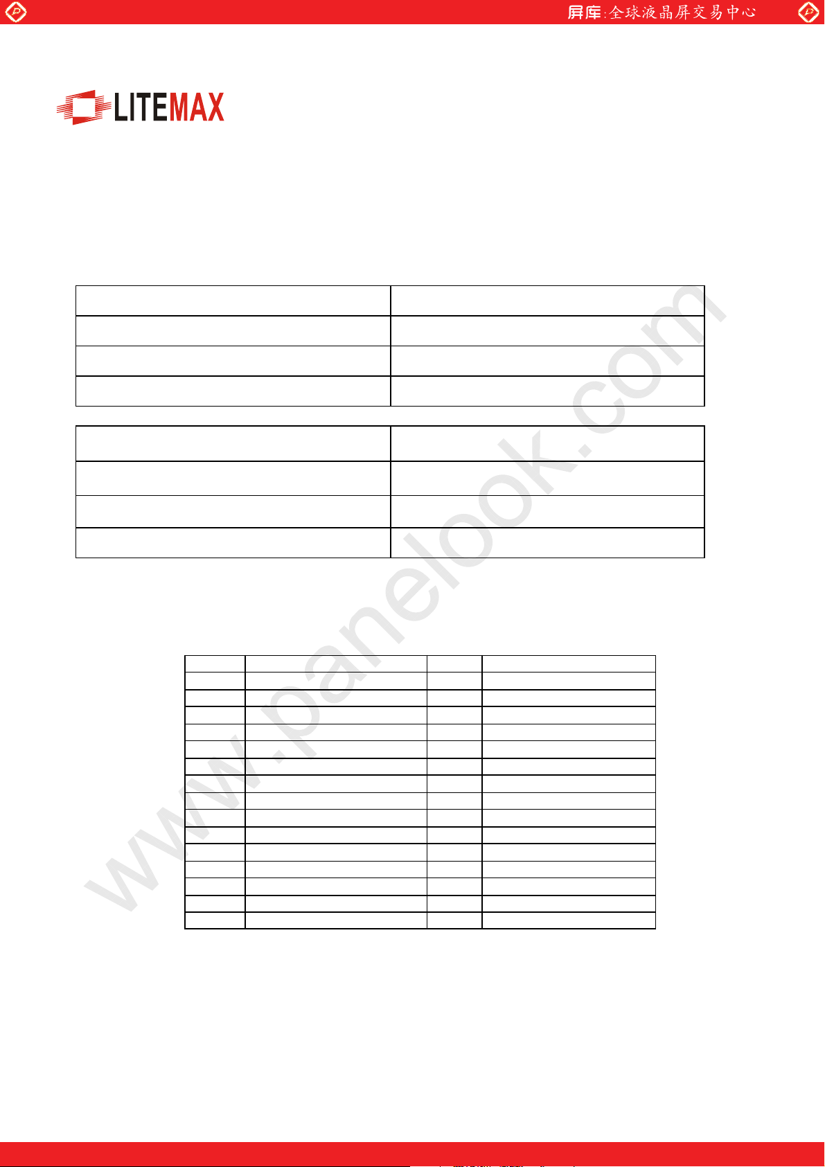
Signal Pin
Pin# Signal Name Pin# Signal Name
1 RxO0- 2 RxO0+
3 RxO1- 4 RxO1+
5 RxO2- 6 RxO2+
7 GND 8 RxOC-
9 RxOC+ 10 RxO311 RxO3+ 12 RxE013 RxE0+ 14 GND
15 RxE1- 16 RxE1+
17 GND 18 RxE219 RxE2+ 20 RxEC21 RxEC+ 22 RxE323 RxE3+ 24 GND
25 NC 26 NC
27 NC 28 Power
29 Power 30 Power
LF1745 Page 10
One step solution for LCD / PDP / OLED panel application: Datasheet, inventory and accessory!
www.panelook.com
Page 11
Global LCD Panel Exchange Center
www.panelook.com
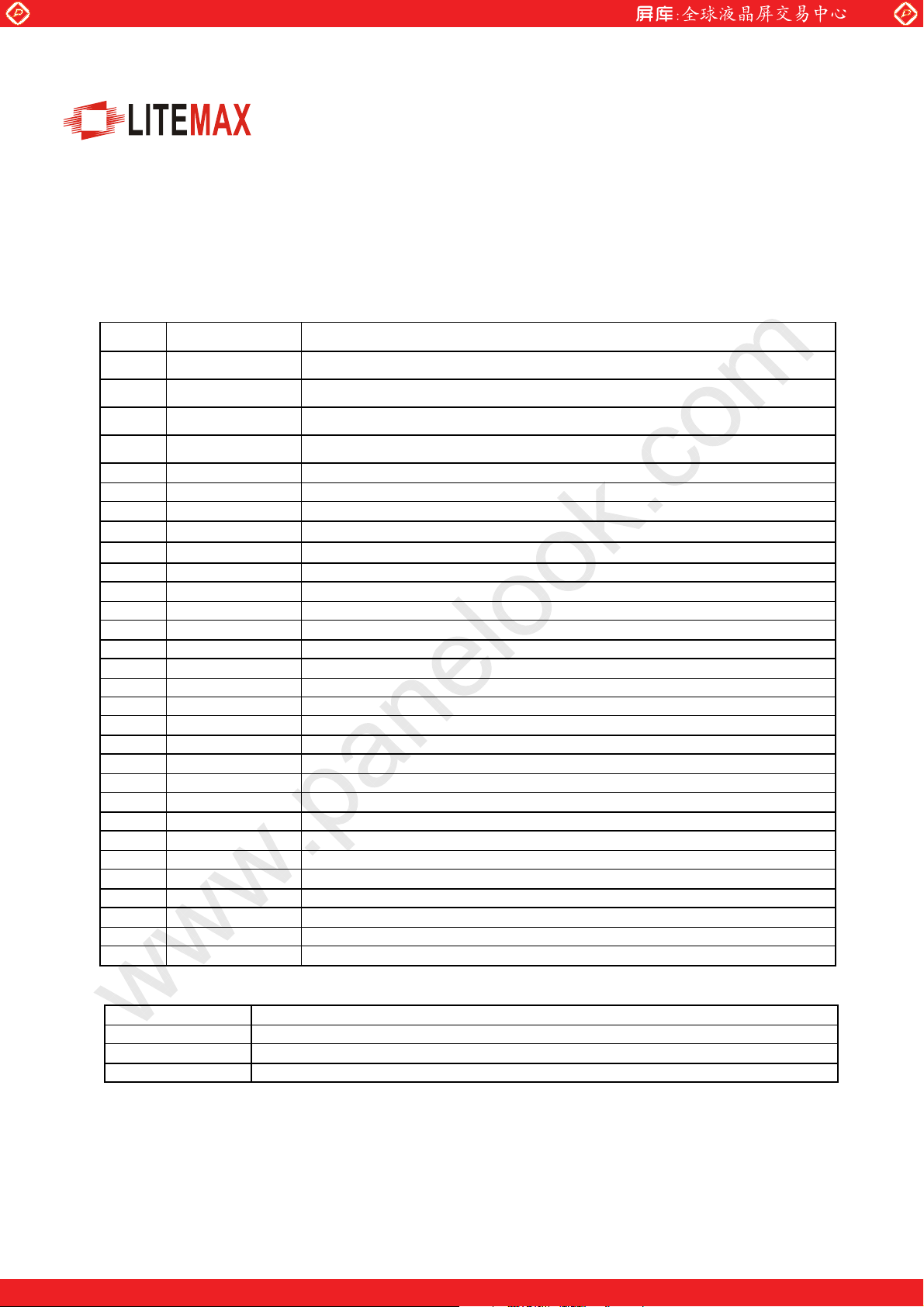
Signal Description
The module using a pair of LVDS receiver SN75LVDS82 (Texas Instruments) or compatible. LVDS is a
differential signal technology for LCD interface and high speed data transfer device. Transmitter shall be
SN75LVDS83(negative edge sampling) or compatible. The first LVDS port(RxOxxx) transmits odd pixels while
the second LVDS port(RxExxx) transmits even pixels.
PIN # SIGNAL NAME DESCRIPTION
1 RxO0- Negative LVDS differential data input (Odd data)
2 RxO0+ Positive LVDS differential data input (Odd data)
3 RxO1- Negative LVDS differential data input (Odd data)
4 RxO1+
5 RxO2- Negative LVDS differential data input (Odd data, H-Sync,V-Sync,DSPTMG)
6 RxO2+ Positive LVDS differential data input (Odd data, H-Sync,V-Sync,DSPTMG)
7 GND Power Ground
8 RxOC- Negative LVDS differential clock input (Odd clock)
9 RxOC+ Positive LVDS differential clock input (Odd clock)
10 RxO3- Negative LVDS differential data input (Odd data)
11 RxO3+ Positive LVDS differential data input (Odd data)
12 RxE0- Negative LVDS differential data input (Even clock)
13 RxE0+ Positive LVDS differential data input (Even data)
14 GND Power Ground
15 RxE1- Positive LVDS differential data input (Even data)
16 RxE1+ Negative LVDS differential data input (Even data)
17 GND Power Ground
18 RxE2- Negative LVDS differential data input (Even data)
19 RxE2+ Positive LVDS differential data input (Even data)
20 RxEC- Negative LVDS differential clock input (Even clock)
21 RxEC+ Positive LVDS differential clock input (Even clock)
22 RxE3- Negative LVDS differential data input (Even data)
23 RxE3+ Positive LVDS differential data input (Even data)
24 GND Power Ground
25 NC 26 NC 27 NC 28 POWER Power
29 POWER Power
30 POWER Power
Note: Input signals of odd and even clock shall be the same timing.
Positive LVDS differential data input (Odd data)
LVDS DATA Name Description
DSP Display Timing: When the signal is high, the pixel data shall be valid to be displayed
V-S Vertical Sync: Both Positive and Negative polarity are acceptable
H-S Horizontal Sync: Both Positive and Negative polarity are acceptable
LF1745 Page 11
One step solution for LCD / PDP / OLED panel application: Datasheet, inventory and accessory!
www.panelook.com
Page 12
Global LCD Panel Exchange Center
Interface connection
www.panelook.com
TI LVDS X’ mitter
SN75LVDS83
Module LVDS signal
(interface connector pin7)
Signal Name Low(open)
D0 Red0
D1 Red1
D2 Red2
D3 Red3
D4 Red4
D5 Red7
D6 Red5
D7 Green0
D8 Green1
D9 Green2
D10 Green6
D11 Green7
D12 Green3
D13 Green4
D14 Green5
D15 Blue0
D16 Blue6
D17 Blue7
D18 Blue1
D19 Blue2
D20 Blue3
D21 Blue4
D22 Blue5
D23 NA
D24 H Sync
D25 V Sync
D26 Display Timing
D27 Red6
LF1745 Page 12
One step solution for LCD / PDP / OLED panel application: Datasheet, inventory and accessory!
www.panelook.com
Page 13
Global LCD Panel Exchange Center
www.panelook.com
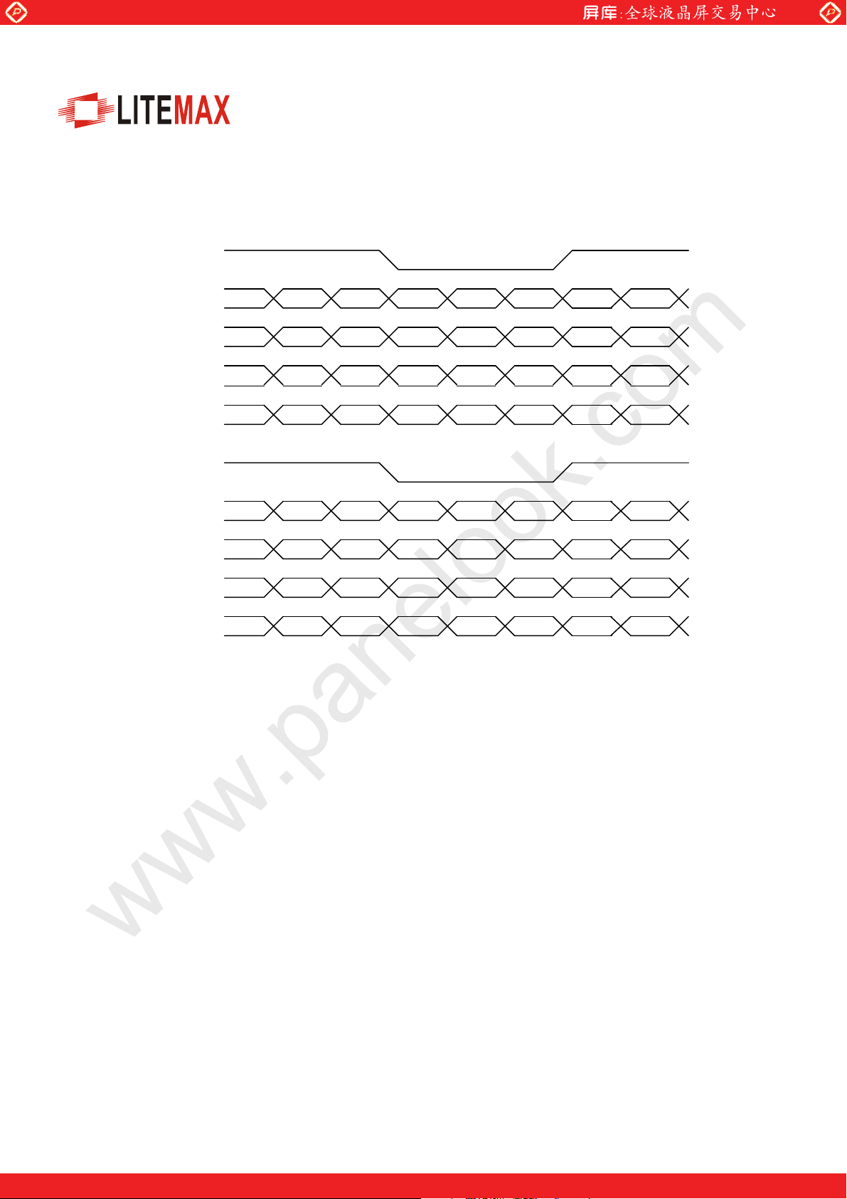
8bits input: M170EN05 only catch bit 2 to bit 7 for 6 bit display
6bits input data format marked with ( ).
RCLKP1
RAP1
RBP1
RCP1
RDP1
G0(0) R5(R3) R4(R2) R3(R1) R2(R0) R1(0) R0(0)
B1(0) B0(0) G5(G3) G4(G2) G3(G1) G2(G0) G1(0)
DE VS HS
RSV
B7(B5) B6(B4) G7(G5) G6(G4) R7(R5) R6(R4)
RCLKP2
RAP2
RBP2
G0(0) R5(R3) R4(R2) R3(R1) R2(R0) R1(0) R0(0)
B1(0) B0(0) G5(G3) G4(G2) G3(G1) G2(G0) G1(0)
RCP2
RDP2
Note: R/G/B data 7:MSB, R/G/B data 0:LSB
O = “ First Pixel Data”
E = “Second Pixel Data”
RSV
B7(B5) B6(B4) G7(G5) G6(G4) R7(R5) R6(R4)
B5(B3) B4(B2) B3(B1) B2(B0)
B5(B3) B4(B2) B3(B1) B2(B0)
LF1745 Page 13
One step solution for LCD / PDP / OLED panel application: Datasheet, inventory and accessory!
www.panelook.com
Page 14
Global LCD Panel Exchange Center
www.panelook.com
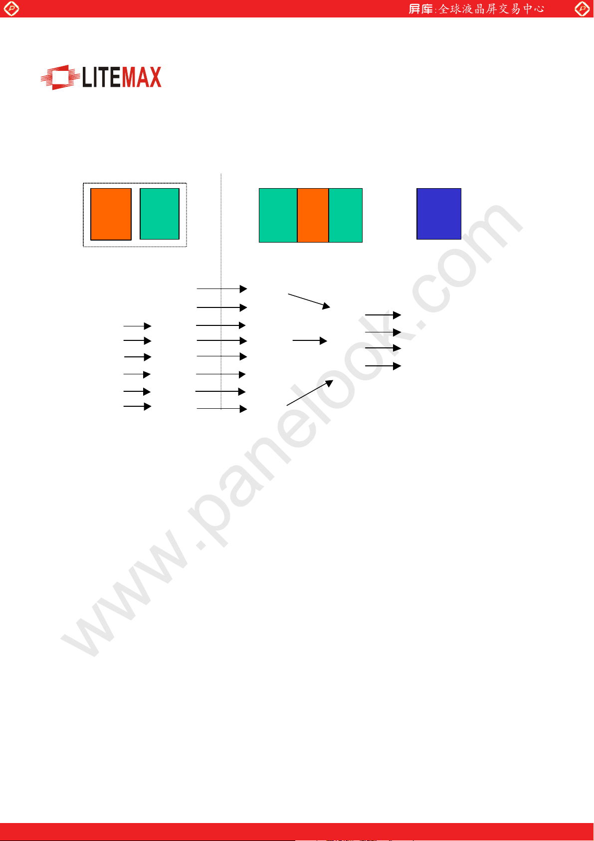
Scaling IC
6 bits+FRC
0
1
2
3
4
5
8 bits LVDS
transmitter
0
1
2
3
4
5
6
7
Controller IC
8 bits LVDS
Receiver
0
1
2
3
4
5
6
7
8 bits RSDS
transmitter
01
23
45
67
M170EN05 moduleLVDS interfaceSystem
Driver IC
6 bits RSDS
receiver driver IC
open
01
23
45
.
LF1745 Page 14
One step solution for LCD / PDP / OLED panel application: Datasheet, inventory and accessory!
www.panelook.com
Page 15
Global LCD Panel Exchange Center
www.panelook.com
Signal Electrical Characteristics
Input signals shall be low or Hi-Z state when Vin is off
It is recommended to refer the specifications of SN75LVDS82DGG (Texas Instruments) in detail.
Each signal characteristics are as follows;
Parameter Condition Min Max Unit
Vth
Vtl
Differential InputHigh
Voltage(Vcm=+1.2V)
Differential Input Low
Voltage(Vcm=+1.2V)
100
-100
[mV]
[mV]
Interface Timings
Basically, interface timings described here is not actual input timing of LCD module but output timing of
SN75LVDS82DGG (Texas Instruments) or equivalent.
Timing Characteristics
Signal Item Symbol MIN TYP MAX Unit
DTCLK Freq. Fdck 50 67.5 70 MHz
DTCLK Cycle Tck 14.2 14.8 20 ns
+V-Sync Frame Rate 1/Tv 56.25 75 77 Hz
+V-Sync Cycle Tv 13 13.33 17.78 ms
+V-Sync Cycle Tv 1035 1066 2047 lines
+V-Sync Active level Tva 3 3 lines
+V-Sync V-back porch Tvb 7 38 63 lines
+V-Sync V-front porch Tvf 1 1 lines
+DSPTMG V-Line m - 1024 - lines
+H-Sync Scan rate 1/Th - 80.06 - KHz
+H-Sync Cycle Th 800 844 1023 Tck
+H-Sync Active level Tha (*1) 4 56 Tck
+H-Sync Back porch Thb (*1) 4 124 Tc k
+H-Sync Front porch Thf 4 24 Tck
+DSPTMG Display Pixels n - 640 - Tck
Note: Typical value refer to VESA STANDARD (*1) Tha+Thb should be less than 1024 Tck.
LF1745 Page 15
One step solution for LCD / PDP / OLED panel application: Datasheet, inventory and accessory!
www.panelook.com
Page 16
Global LCD Panel Exchange Center
Timing Definition
www.panelook.com
1688dot
H-Sync
DSPTMG
V-Sync
D
PTM
4
24
112dot
1280dot
1H
38H
H
Power Consumption
Input power specifications are as follows;
Symbol Parameter Min Typ Max Units Condition
VDD Logic/LCD Drive
Voltage
IDD VDD current 950 1200 [mA]
PDD VDD Power 4.75 6.6 [Watt] Vin=5V, All Black Pattern
VDDrp Allowable
Logic/LCD Drive
Ripple Voltage
VDDns Allowable
Logic/LCD Drive
Ripple Noise
4.5 5 5.5 [Volt]
100 [mV]
p-p
100 [mV]
p-p
LF1745 Page 16
One step solution for LCD / PDP / OLED panel application: Datasheet, inventory and accessory!
www.panelook.com
Page 17
Global LCD Panel Exchange Center
www.panelook.com
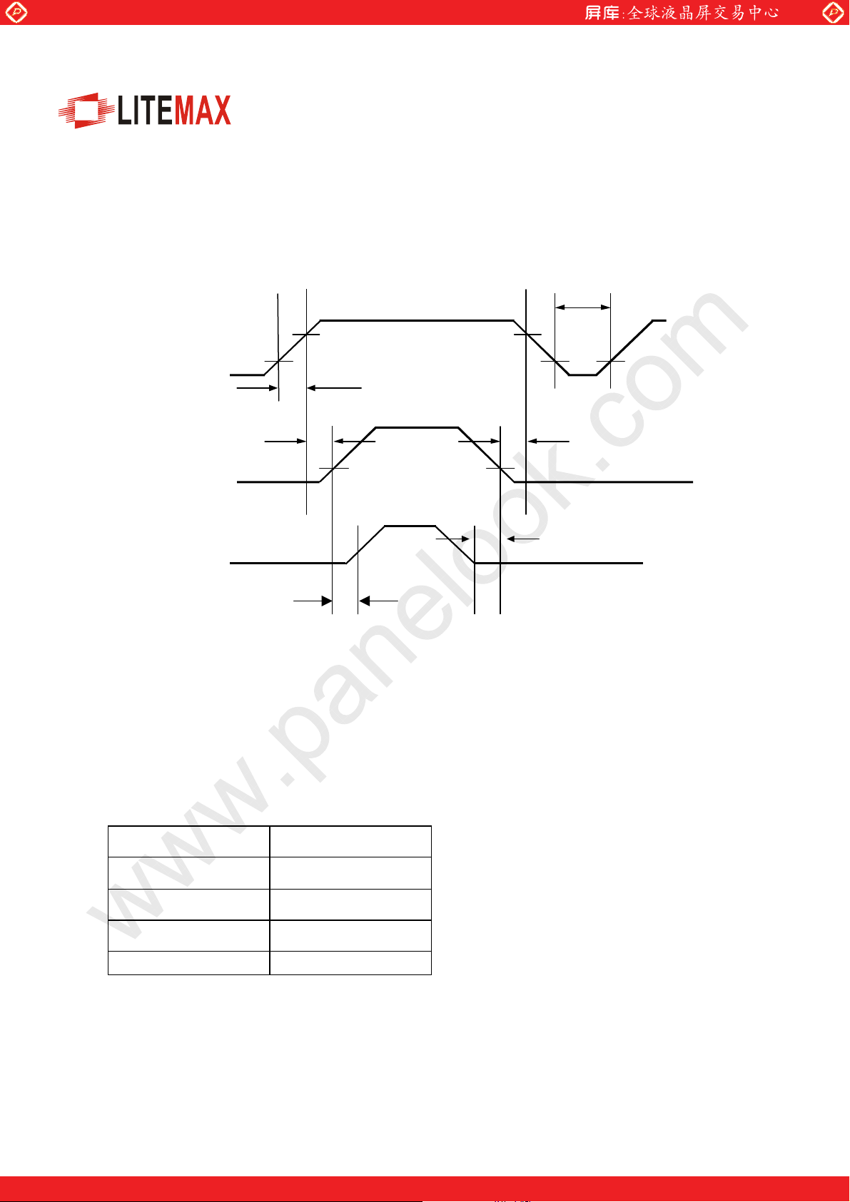
Power ON/OFF Sequence
Vin power and lamp on/off sequence is as follows. Interface signals are also shown in the chart. Signals from
any system shall be Hi-Z state or low level when Vin is off.
1sec
min.
Vin
10%
0 V
Signal
0 V
Lamp
On
0 V
Backlight Characteristics
90% 90%
15ms max.
10%10%
250ms
10%
10%
0 min.0 min.
0 min.
Signal for Lamp connector
Pin # Signal Name
1 Lamp High Voltage
2
3
4
LF1745 Page 17
Lamp High Voltage
No Connection
Ground
One step solution for LCD / PDP / OLED panel application: Datasheet, inventory and accessory!
www.panelook.com
Page 18
Global LCD Panel Exchange Center
www.panelook.com
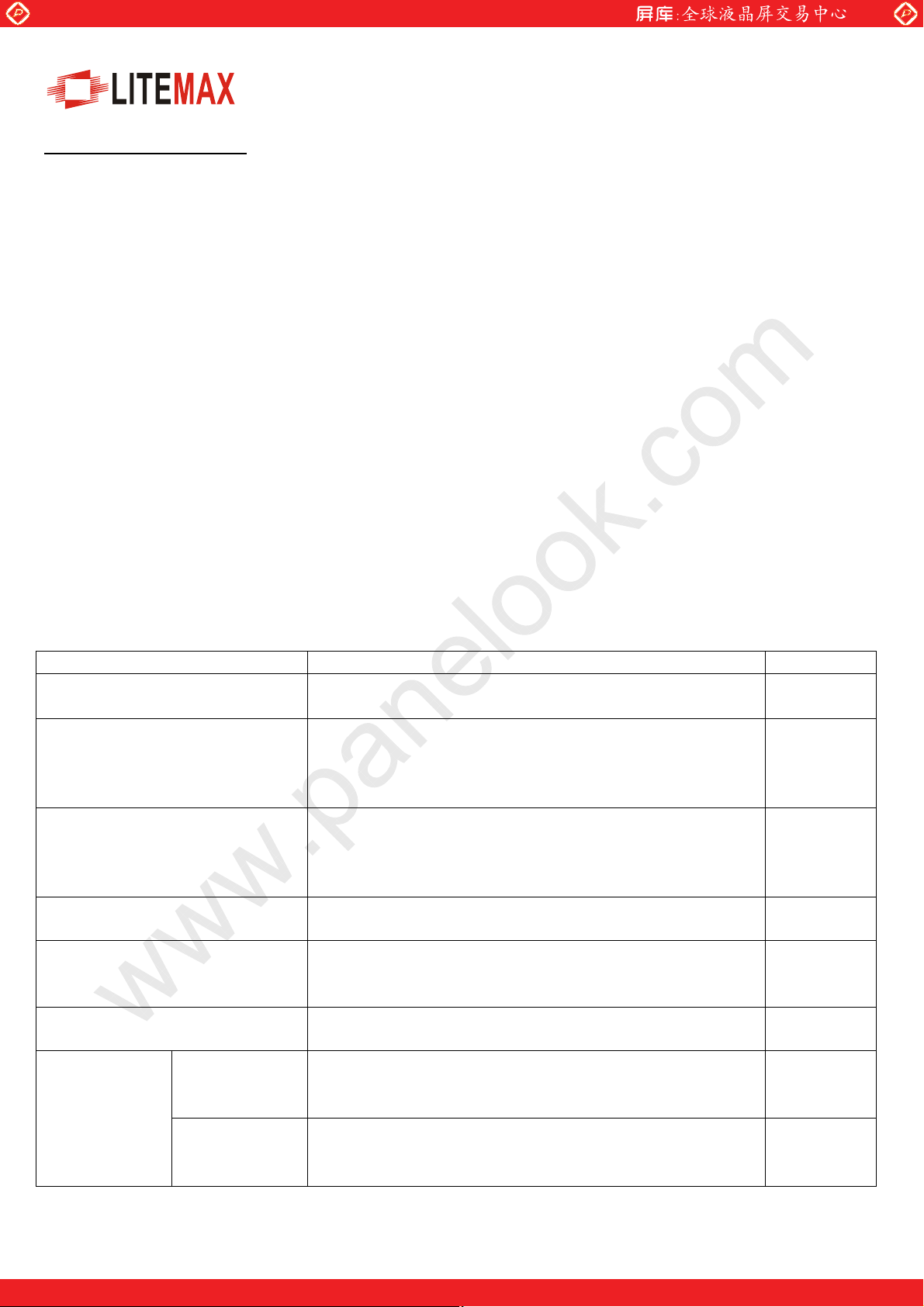
Reliability and Lifetime
Monitor Reliability
Demostrated MTTF testing in progress
Backlight Reliability and Lifetime
CCF lamps; 40,000 hour rated lifetime @ 25qC
CCF lamp life is defined as time to 50% of initial brightness
Backlight end-of-life for this 1745 product is defined as 1000 nits center luminance at 25qC
Typical values indicated for luminance and uniformity are indicative of typical steady state values
measured at initial use at 25qC after warm-up to steady state. Actual luminance and uniformity values
are directly dependent on the environmental usage profile. Repeated cold temperature start-up can
cause accelerated aging of the backlight lamps resulting in reduced luminance and uniformity.
Extended High Temperatures and Solar Loading
Extended operation at the upper temperature extreme or in conjunction with extended direct solar
loading can cause permanent mura or localized pixel non-uniformity effects. Other side effects could
include latent image and flicker. These effects are not covered under Litemax warranty. Please
consult Litemax for further guidance on system design to effectively manage environments requiring
extended high temperatures or direct sun-loading. Cooling kit and CEG vandal glass options can
effectively address these issues.
Reliability Test
Test Item Test ondition Judgement
High temperature/humidity
operation
Heat cycle (operation)
1. 60±2qC, RH=60%, 240 hours,
2. Display data is white.
1. 0qC±3qC…1 hour
2. 55qC±3qC…1 hour
Note 1
Note 1
3. 50 cycles, 4 hours/cycle
4. Display data is white.
Note 1
Thermal shock (non-operation)
1. -20qC±3qC…1 hour
2. 60qC±3qC…1 hour
3. 100 cycles, 4 hours/cycle
4. Temperature transition time is within 5 min.
Vibration (non-operation) 5-100Hz, 11.76m/s2, 1 minute/cycle, XYZ direction
Note 1
10 times each direction
ESD (non-operation)
150pF, 150:, ±10kV
Note 1
9 places on a panel (Note 3)
10 times each place at one-second intervals
Dust (non-operation) Sample dust: No.15
Note 1
Hourly 15 seconds stir, 8times repeat
operation 53.3 kPa
Note 1
0qC±3qC…24 hours
Low pressure
non-operation 15 kPa
55qC±3qC…24 hours
Note 1
-20qC±3qC…24 hours
-60qC±3qC…24 hours
LF1745 Page 18
One step solution for LCD / PDP / OLED panel application: Datasheet, inventory and accessory!
www.panelook.com
Page 19
Global LCD Panel Exchange Center
www.panelook.com
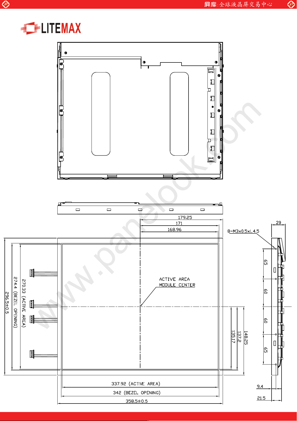
Mechanical Characteristics
One step solution for LCD / PDP / OLED panel application: Datasheet, inventory and accessory!
LF1745 Page 19
www.panelook.com
Page 20
Global LCD Panel Exchange Center
www.panelook.com
LITEMAX LI3601 inverter
Introduction
LI3601 is a CCFL inverter to operate LITEMAX high brightness (HB) backlights. The inverter
has an on-board pulse width modulation (PWM) dimming circuit for extremely wide range
luminance adjustment. Over the entire dimming range, there is no noticeable lamp flickering
and the uniformity of the backlight is well maintained. When using LI3601 with LITEMAX LCD
modules, it is not necessary to synchronize the PWM circuit to vertical sync signal of the LCD.
Dimming Control
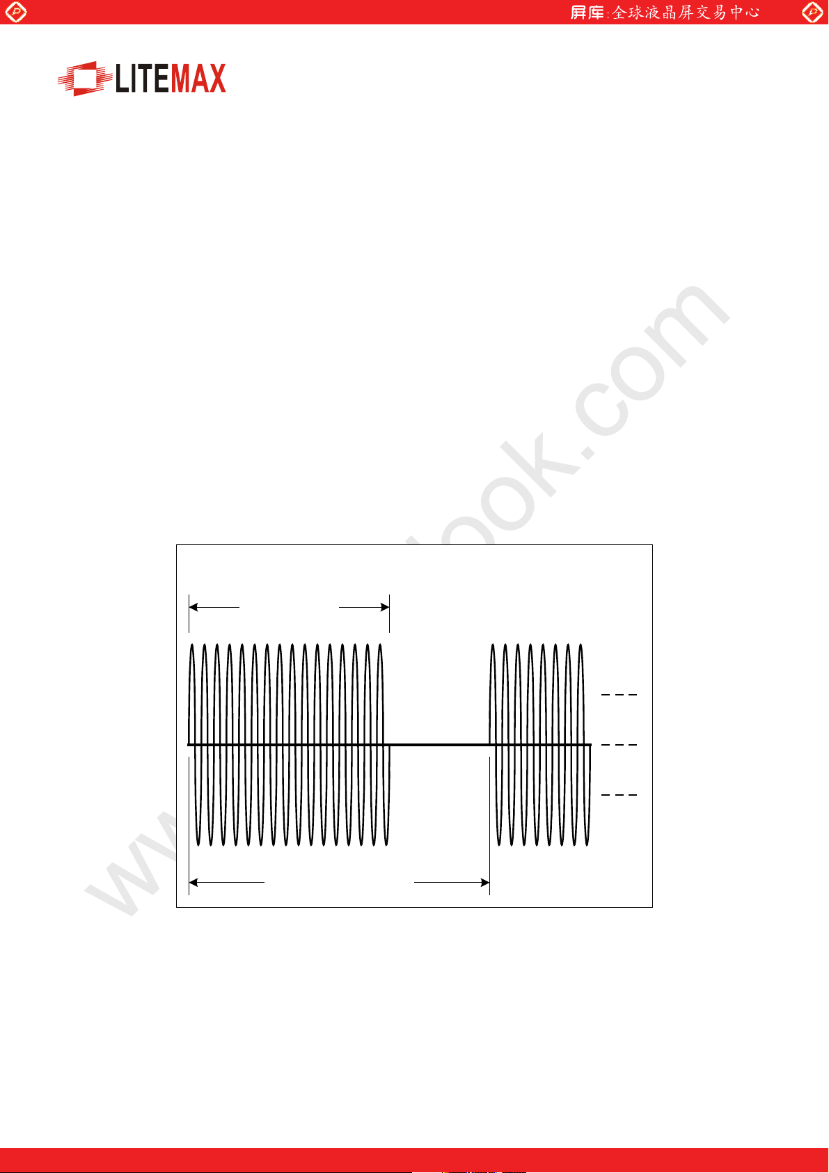
The LI3601 accepts a 0V to 5V analog voltage for dimming control. It has a pulse width
modulation (PWM) dimming circuit for luminance adjustment. As the dimming voltage (Vd)
decreases from +5V, the lamp current waveform is pulse width modulated at a repetition rate
high enough to prevent LCD flicker. Within each PWM cycle, the lamps in the backlight are
turned fully 'ON' for a fraction of the cycle time. The human eyes, being very slow with respect
to the PWM rate, respond to the average light produced over the PWM cycle. As a result, the
luminance of the backlight and/or the LCD screen is approximately to the duty cycle of the
PWM waveform.
Lamp Current Waveform
t (lamp on)
T (1 PWM cycle) Duty Cycle = t / T
The lamp current waveform with the PWM circuit set at less than 100%
LI3601 Inverter Page 20
One step solution for LCD / PDP / OLED panel application: Datasheet, inventory and accessory!
www.panelook.com
Page 21
Global LCD Panel Exchange Center
www.panelook.com
In general, inverters with PWM dimming have a very wide luminance adjustment range. For
most practical cases, the LI3601 inverter can achieve a dimming ratio up to 200:1. Hence, the
luminance of the backlight or LCD screen can be adjusted from 100% to 0.5%.
The 0V to 5V dimming voltage can be generated simply by a potentiometer, by a digitally
controlled UP/DOWN counter or a digital potentiometer. The inverter provides a regulated +5V
supply to power the dimming circuit. However, the maximum current drain from this source
should be kept less than 5 mA.
At a Vd input about 0.34V and less, the duty cycle of the PWM waveform is 0% and thus, the
lamps are 'OFF'. In order to fully utilize the available dimming voltage, Vd should be biased to
about 0.34V and then ramping up to 5.0V.
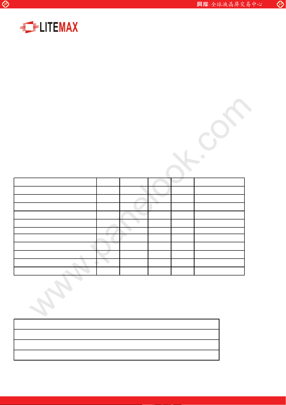
Electrical Characteristics
The LI3601 inverter operates at 12V DC and can drive up to 12 lamps for a maximum output
power about 63 Watts. In addition, the inverter has a regulated +5V output serving as a voltage
source for the dimming control circuit.
Electrical Characteristics
Parameters Min Typ Max Units Conditions
Input Voltage (Vin) 11.5 12 12.5 Vdc
Input current (I) 5.25 Adc Vin=12, Vd=5 V
Lamp Starting Voltage (Vst) 1300 Vrms Vin=12, Vd=5 V
Frequency (f) 55 58 60 Khz
ON/OFF Control -OFF 0.2 Vdc
-ON Floating*
Dim ming Voltage(Vd)
@ 100% Duty Cycle 4.9 5 Vdc Max brightness
@ 0% Duty Cycle 0.34 0.36 Vdc Zero brightness
5V Output (+5VOUT) 4.85 5 5.25 Vdc 11.5<Vin<12.5V
5V Output Source Current 5 mA
*Please refer to Application Note AN001 for details of On/Off control and dimming control with an external PWM
signal.
Absolute Maximum Rating
Parameters Min Max Units
Inverter Input Voltage (Vin) 11 13 Vdc
Operating Temperature Range 0 50 C
Storage Temperature Range -20 80 C
LI3601 Inverter Page 21
One step solution for LCD / PDP / OLED panel application: Datasheet, inventory and accessory!
www.panelook.com
Page 22
Global LCD Panel Exchange Center
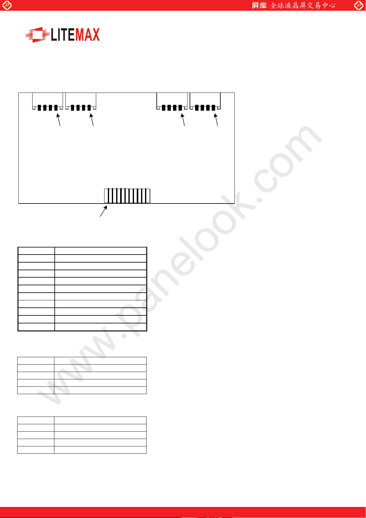
Interface Connector
pin1 pin1pin1 pin1
CN1
www.panelook.com
J2J1J3J4
pin 1
Input Connector (CN1)
Pin# Function
1 5V Output
2 12V Input
3 12V Input
4 Dimming Control
5 Ground
6 Ground
7 ON/OFF Control
8NC
9 PWMCTRL
10 NC
Output Connector (J2, J3)
PIN# Function
1 Lamp Connection
2 Lamp Connection
3 Lamp Connection
4 NC
Output Connector (J1, J4)
PIN# Function
1 Lamp Connection
2 Lamp Connection
3 NC
4 Lamp Common
LI3601 Inverter Page 22
One step solution for LCD / PDP / OLED panel application: Datasheet, inventory and accessory!
www.panelook.com
Page 23
Global LCD Panel Exchange Center
r
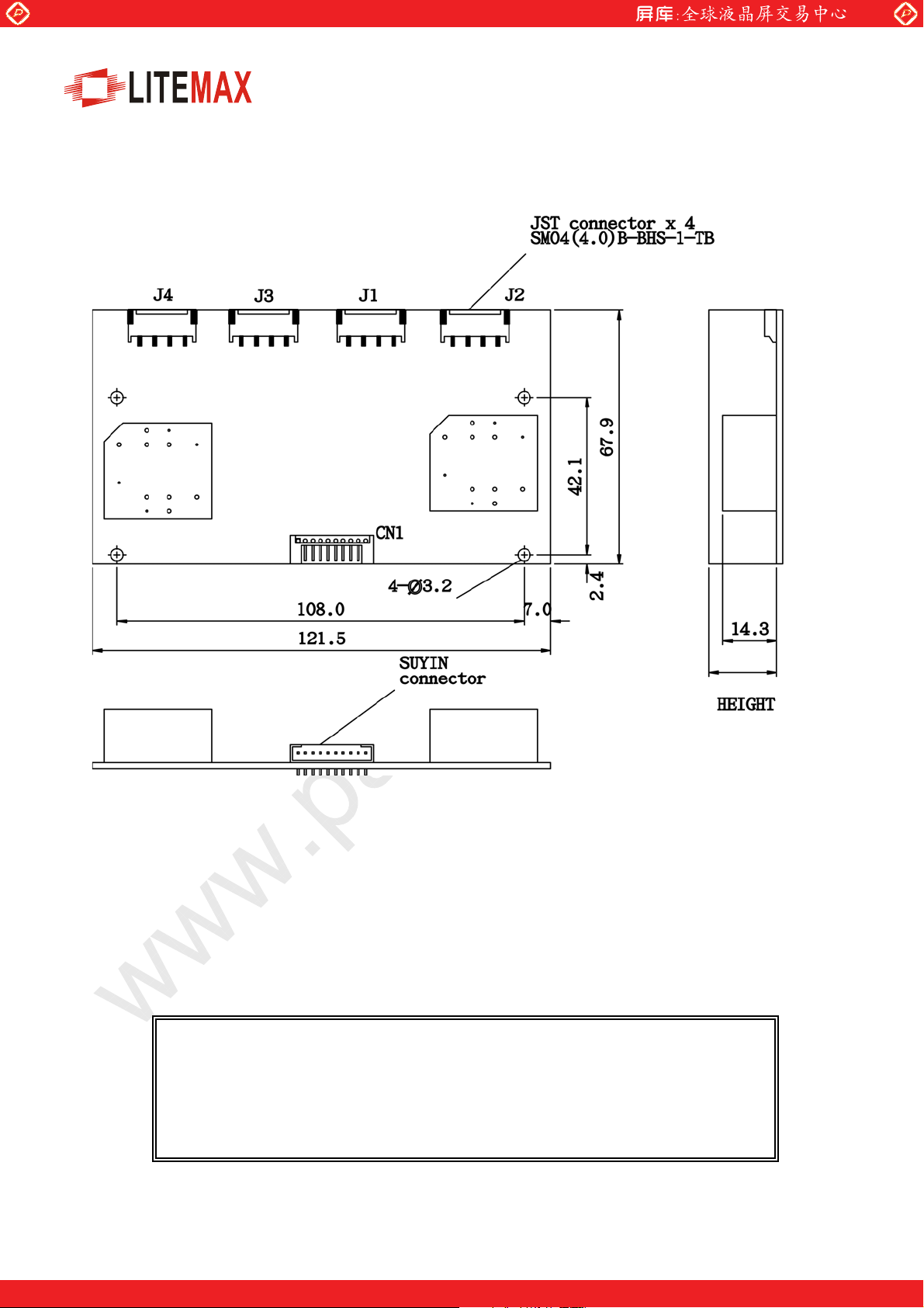
Mechanical
www.panelook.com
LITEMAX Electronics Inc. reserves the right to make changes to this document and the
product, which it describes without notice. LITEMAX Electronics Inc. also shall not be
liable for technical or editorial errors or omissions made herein; nor for incidental o
consequential damages resulting from the furnishing, performance, or use of this
product. In addition, LITEMAX Electronics Inc. takes no responsibility for damage
caused by improper use of this product, which does not meet the conditions for use
specified in this specification sheet.
LI3601 Inverter Page 23
One step solution for LCD / PDP / OLED panel application: Datasheet, inventory and accessory!
www.panelook.com
 Loading...