

Page 1
LS-WIFI
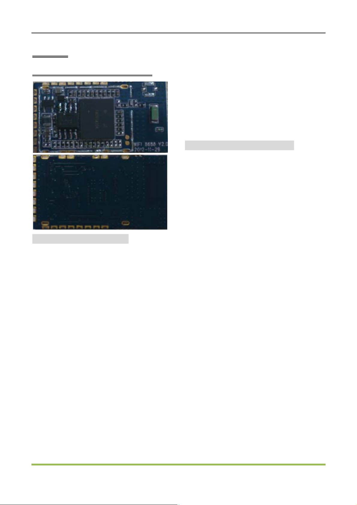
8688 Module Specification
1 Features
■ Qualified 2.4-GHz IEEE 802.11b/g transceiver
■ Address the connectivity demand in M2M
applications, e.g. UART-WiFi Bridge, WiFi
Gateway, Wireless Sensor Node and etc
■ ARMv5TE-compliant MCU running up to
106MHz
■ Ultra-low power: 4 uA sleep, 40 mA Rx, 210 mA
Tx
■ Receive sensitivity:
• -87 dBm @ b mode
• -72.5 dBm @ g mode
■ Maximum Couducted Peak output power:
• 16 dBm @ b mode
• 16 dBm @ g mode
■ High throughput, 1 Mbps sustained data rate
with TCP/IP and WPA2
■ Small, compact surface-mount module
■ On-board ceramic chip antenna
■ UART hardware interface
■ Supports ad hoc and infrastructure networking
modes
■ On board ECOS -OS, TCP/IP stacks
■ Wi-Fi Alliance certified for WPA2-PSK
■ FCC/CE/ICS certified and RoHS compliant.
Applications
■ Remote equipment monitoring
■ Telemetry
■ Industrial sensors and home automation
controls
■ Medical device monitoring
2 Overview
2.1 Description
The LS-WIFI8688 module is a standalone,
embedded wireless 802.11 b/g networking module.
With its small form factor and extremely low power
consumption, the LS-WIFI8688 is perfect for
mobile wireless applications such as asset
monitoring, GPS tracking, and battery sensors.
The WiFl module incorporates a 2.4-GHz radio,
processor, TCP/IP stack, crypto accelerator,
power management, and analog sensor interfaces.
The module is preloaded with software to simplify
integration and minimize application development.
In the simplest configuration, the hardware
requires only four connections (PWR, TX, RX, and
GND) to create a wireless data connection.
Additionally, the sensor interface provides
temperature, audio, motion, acceleration, and
other analog data without requiring additional
hardware. The module is programmed and
controlled with a simple ASCII command
language.
Once the module is set up, it can scan to find an
access point, associate, authenticate, and
connect over any Wi-Fi network.
2.2 Overview
■ Host data rate up to 1 Mbps for the UART
‐1‐/16
Page 2
■ Intelligent, built-in power management with
programmable wakeup
■ Real-time clock for time stamping, auto-sleep,
and auto-wakeup
■ Configuration over UART using simple ASCII
commands
■ Remote configuration over WiFi using Telnet
■ Supports over the air firmware upgrade (FTP)
■ Supports WPS pushbutton mode for easy
association with access points
■ Secure WiFi authentication using WEP-128,
WPA-PSK (TKIP), or WPA2-PSK (AES)
■ Built-in networking applications—DHCP, UDP,
DNS, ARP, ICMP, TCP, HTTP client, and FTP
client
■ 802.11 power saving and roaming functions
■The modules size:
Size: 32mm x 17.5 mm x 3.0 mm
3 Electrical characteristics
3.1 DC/RF CHARACTERISTICS
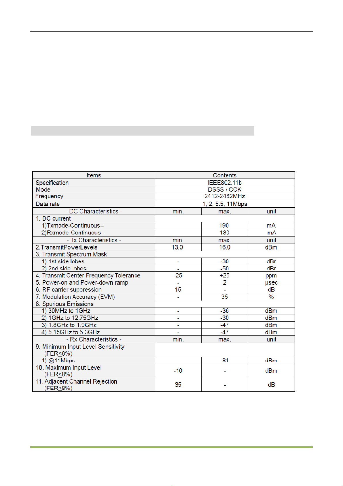
3.11 Characteristics for IEEE802.11 b
‐2‐/16
Page 3
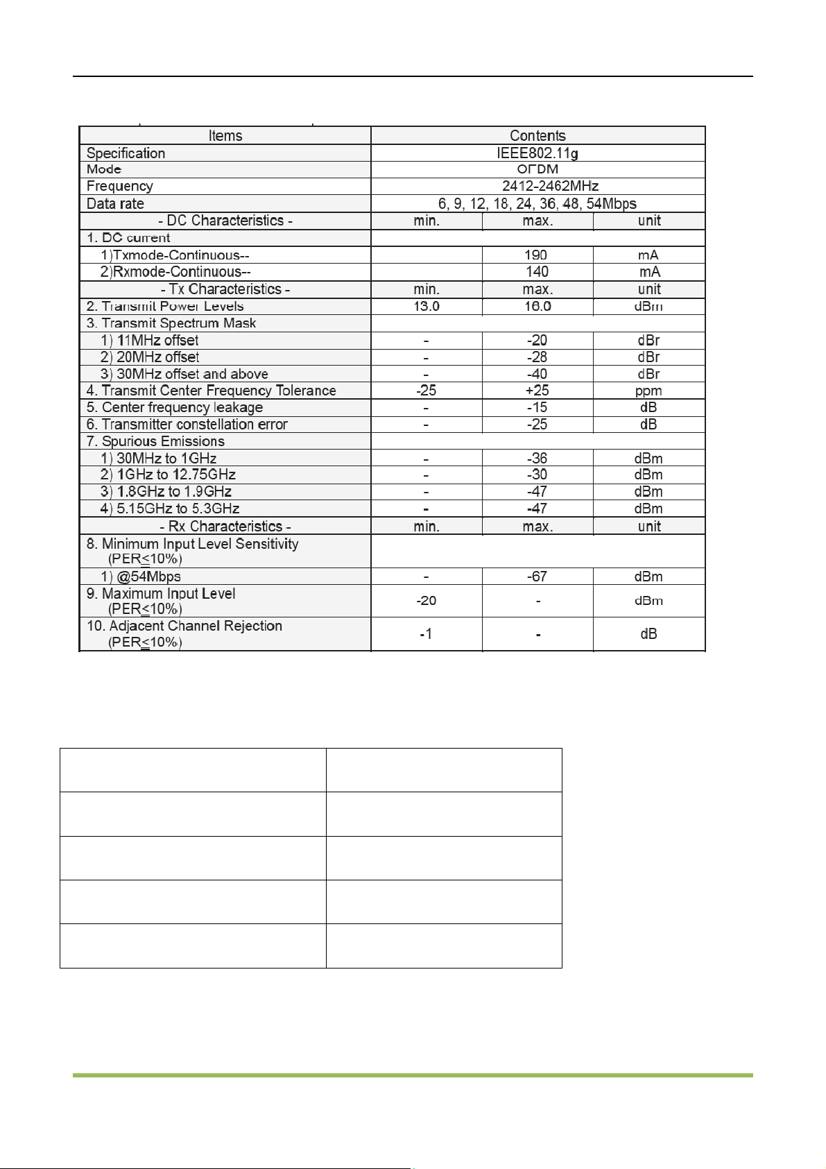
3.12 Characteristics for IEEE802.11g
3.2 Environmental Conditions
Parameter WiFi 8688
Temperature Range(Operating)
Temperature Range(Storage)
Relative Humidity(Operating) ≤90%
Relative Humidity(Storage) ≤90%
-20℃ to +70℃
-40℃ to +85℃
3/16
Page 4
3.3 Absolute maximum ratings
Parameter Minimum Maximum Unit
VDD33 -0.3 3.9V V
GND - 0 V
I/O pin voltage -0.3 VDD33+0.3V V
3.4 Operating conditions
Symbol Parameter min Nominal Max Unit
VDD33 Supply voltage 3.1 3.3 3.6 V
VIH
VIL
VOH
VOL
I/O input high voltage 2.3 - Vdd33+0.3 V
I/O input low voltage -0.3 - 1.1 V
I/O output high voltage 2.57 - - V
I/O output low voltage - - 0.4 V
4 Pin-out and signal description
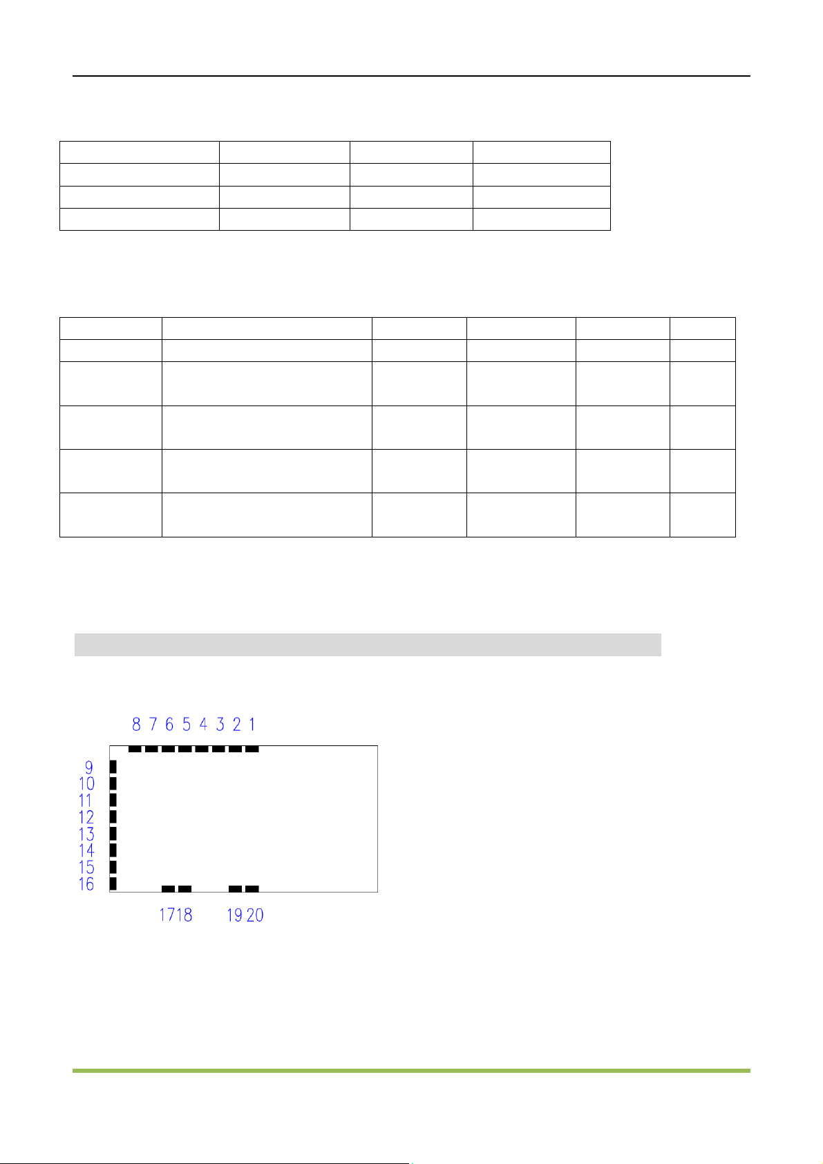
4.1 Pin Pads(Top View):
4/16
Page 5

4.2 Pin Description:
No. Terminal Name Type System
1 GND G - VSS Ground
2 NC - -
3 UART_SIN I/O -
4 UART_SOUT I/O -
5 NC - -
6 GND G - VSS Ground
7 VDD33 VDD33 - VDD33 3.3V Power Supply
8 GND G - VSS Ground
SPI_CLK_REQ/
9
SD_DAT[3]
I/O WLAN
Connection to
IC Terminal
SPI_CLK_REQ/
SD_DAT[3]
Description
UART SIN input
When not used, this pin should be left
floating.
UART SOUT outpup
When not used, this pin should be left
floating.
G-SPI Mode: SPI_CLK_REQ
G-SPI Clock Request
SDIO 4-bit Mode: SD_DAT[3]
Data Line Bit[3]
SDIO 1-bit Mode: SD_DAT[3]
Reserved
SDIO SPI Mode: SD_DAT[3]
Card Select (active low)
10
5/16
SPI_SINTn/
SD_DAT[2]
I/O WLAN
SPI_SINTn/
SD_DAT[2]
G-SPI Mode: SPI_SINTn
G-SPI Interrupt Output (active low)
SDIO 4-bit Mode: SD_DAT[2]
Data Line Bit[2] or Read Wait (optional)
SDIO 1-bit Mode: SD_DAT[2]
Read Wait (optional)
SDIO SPI Mode: SD_DAT[2]
Reserved
Page 6

11
12
13
14
SPI_SDO/
SD_DAT[1]
SPI_SCSn/
SD_DAT[0]
SPI_SDI/
SD_CMD
SPI_CLK/
SD_CLK
I/O WLAN
IO WLAN
I/O WLAN
I WLAN
SPI_SDO/
SD_DAT[1]
SPI_SCSn/
SD_DAT[0]
SPI_SDI/
SD_CMD
SPI_CLK/
SD_CLK
G-SPI Mode: SPI_SDO
G-SPI Data Output
SDIO 4-bit Mode: SD_DAT[1]
Data Line Bit[1]
SDIO 1-bit Mode: SD_DAT[1]
Interrupt
SDIO SPI Mode: SD_DAT[1]
Reserved
G-SPI Mode: SPI_SCSn
G-SPI Chip Select input (active low)
SDIO 4-bit Mode: SD_DAT[0]
Data Line Bit[0]
SDIO 1-bit Mode: SD_DAT[0]
Data Line
SDIO SPI Mode: SD_DAT[0]
Data Output
G-SPI Mode: SPI_SDI
G-SPI Data Input
SDIO 4-bit Mode: SD_CMD
Command/Response
SDIO 1-bit Mode: SD_CMD
Command Line
SDIO SPI Mode: SD_CMD
Data Input
G-SPI Mode: SPI_CLK
G-SPI Clock Input
SDIO 4-bit Mode: SD_CLK
Clock Input
SDIO 1-bit Mode: SD_CLK
Clock Input
SDIO SPI Mode: SD_CLK
Clock Input
15 SLEEP_CLK I WLAN SLEEP_CLK Clock Input for External Sleep Clock
16 RESETn I - RESETn Reset (active low)
17 GND G - VSS Ground
18 GND G - VSS Ground
19 GND G - VSS Ground
20 GND G - VSS Ground
6/16
Page 7
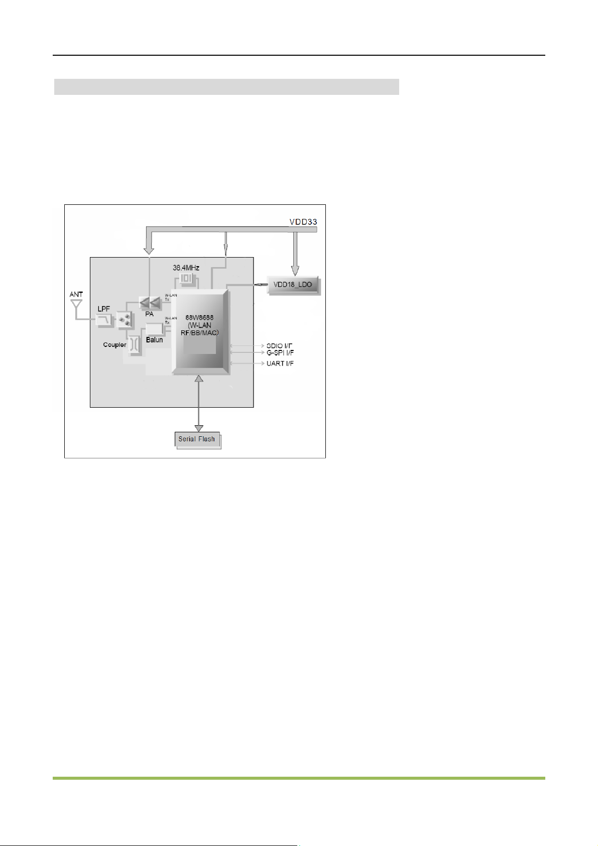
5 Functional description
5.1 Functional block diagram
5.2 RF descriptions
The LS8688 is equipped with a fully integrated RF to baseband transceiver that operates in both the 2.4
GHz ISM radio band for 802.11g/b WLAN applications,It contains all the circuitry to support both transmit
and receive operations.
5.3 On-board antenna specification
The LS8688 contains a chip multilayer antenna.
Part Number: LDA312G4413H-280.
Manufacturer: Murata.
Gain: 0.1 dBi
7/16
Page 8
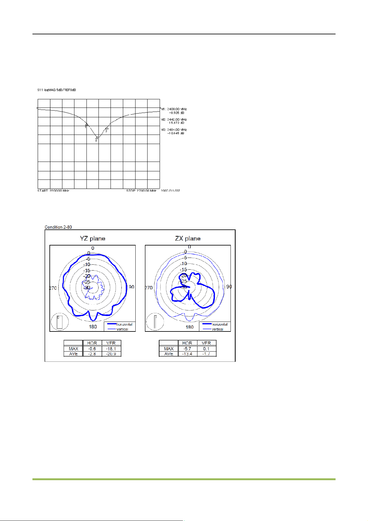
5.3.1 Return Loss
5.3.2 Radiation Pattern
5.4 Clock specifications
LS8688 has a high-speed 38.4MHz oscillator to provide clock signals for the processors. The customer
doesn’t need to use external CLK.
8/16
Page 9
5.5 UART host interface
The LS8688 supports a high speed Universal Asynchronous Receiver/Transmitter (UART) interface.
High speed baud rates are supported to provide the physical transport between the device and the
host for
wireless data connection. Customer can use AT command to control the module.
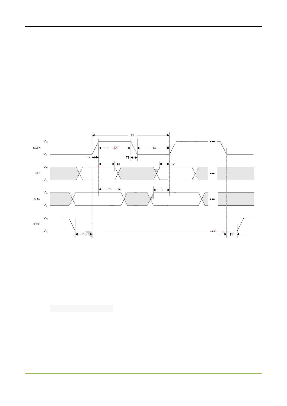
5.6 G-SPI host interface specifications
Referred from Marvell hardware specifications
G-SPI Host Interface Transaction Timing
5.7 Power supply description
The LS8688 contains a high efficiency DC/DC converter to reduce power consume and
simplified peripheral circuit design, external only need 3.3V voltage to input to pin 7 of
LS8688. the converter generate 1.8V voltage for core of 88W8688. The converter is
composed of XC9216A18MCR and inductor LQG15HS10NJ02, Efficiency >85%, Output
Current >400mA.
9/16
Page 10
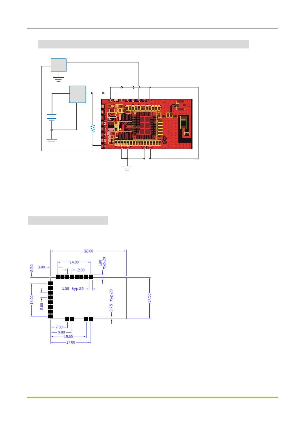
6 Typical application schematic
HOST
Regulator
UART RXD_
UART TXD_
33V.
10KΩ
7 Package
Module Physical Dimensions (unit: mm)
Note: the LS8688 is without shielding box.
10/16
Page 11
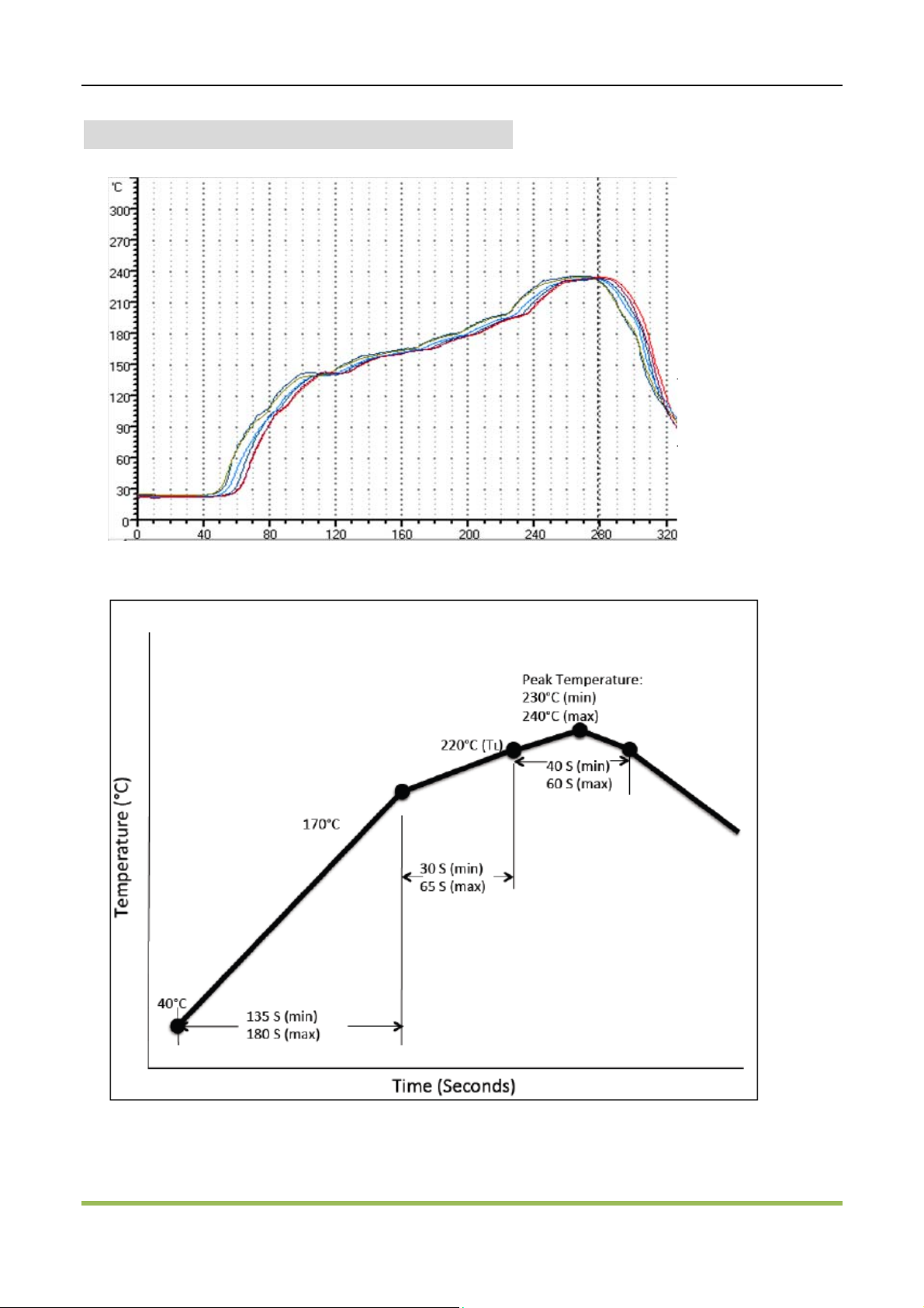
8 Solder reflow temperature profile
11/16
Page 12

9 AT Command
1.help(All the commands of the system support will be listed)
Input: *AT*help*
Output:
sdk-version
psm-register<module><partition-key>
psm-get<module><variable>
psm-set<module><variable><value>
psm-erase
psm-dump<partition_no>
psm-get-free-space<module>
rfprint<http_url>
updatefw<http_url>
updatefs<http_url>
sysinfo [see sysinfo -h for details]
START Start network connection
STOP Stop network connection
APN Set or get default AP: <profile_name>ssid<ssid> [bssid<bssid>]
SERV Set or get Server IP info: <IP>, <Port>, <Index>
wlan-scan
wlan-stat
wlan-info
wlan-gethostbyname<hostname>
2.wlan-scan(Scan the AP)
Input: *AT*wlan-scan*
Output:
The current AP(include:SSID, BSSID,channel,rssi,security,WMM)
For example:
+wlan-scan:OK
2 networks found:
AP[1]
SSID: cer-test
Mode: infra
channel: 1
rssi: -50 dBm
security: WPA
WMM: NO
AP[2]
SSID: h3c
12/16
Page 13

Mode: infra
channel: 1
rssi: -50 dBm
security: OPEN
WMM: NO
3.APN (Setup all demand the AP)
(1).Demand the setting of current AP:
Input:*AT*APN*?*
Output:+APN:OK
profile=<profile name>,ssid=<apssid>,mode=<[infra][ad-hoc]>,security=<security type>
For example:
+APN:OK
profile=default,ssid=h3c,mode=infra, security=None
(2).Setup AP:
Input:*AT*APN*<profile name>ssid<SSID>[wep/wpa/wpa2] [password]
For ”OPEN” network, the command format: <profile_name>ssid<ssid> [bssid<bssid>]
For security ”WEP” network, the command format: <profile_name>ssid<ssid>wep open <WEP_key>
For security ”WPA/WPA2” network, the command format: wlan-add <profile_name>ssid<ssid> wpa2
<secret>
Note:”profile name” is the configure name, It can be any name.
For example:
◆Connect to the AP(SSID:h3c, Security: None, profile name: default)
Input: *AT*APN*defaultssid h3c*
Output:+APN:OK
Name=default, SSID=h3c,Mode=infra, Security=None
◆Connect to the AP(SSID: SyChip-Network, Security: WPA2, password: xxxxxxxx, profile name: net)
Input: *AT*APN*net ssid SyChip-Network wpa2 xxxxxxxx*
Output:+APN:OK
Name=net, SSID=SyChip-Network, Mode=infra, Security=WPA2
◆When name the static IP address information (include IP address, Subnet mask, Default gateway), use
the command format as follows:
*AT*APN*<profile_name>ssid<ssid>ip:<ip_addr>,<gateway_ip>,<netmask>*
Input:*AT*APN*defaultssid h3c ip:10.3.2.123, 255.255.0.0, 10.3.1.2*
Output:+APN:OK
Name=default,SSID=h3c,Mode=infra,Security=None
4.wlan-stat(Display the state of the current wlan)
Input:*AT*wlan-stat*
13/16
Page 14

Output: disconnected, connecting or Connected。
5.wlan-info(Display the information of the current wlan, include SSID, Encryption, IP address)
Input:*AT*wlan-info*
Output:
◆(If the profile name=Provisioning, SSID= PROV-24-A6-90, Then output:)
+wlan-info:OK
Profile: provisioning
SSID: PROV-24-A6-90
BSSID: 5C:DA:D4:24:A6:90
channel: 11
mode: adhoc
security: WEP (shared)
address: STATIC
IP:192.168.10.1
gateway:192.168.10.1
netmask:255.255.255.0
dns1:192.168.10.1
dns2:192.168.10.1
◆(If disconnected to AP, Then output:)
Not connected
6. wlan-mac(Demand the MACID)
Command format:*AT*wlan-mac *
Input:*AT*wlan-mac *
Output:5C:DA:D4:24:A6:90
7. wlan-gethostbyname (Parse Hostname)
Command format:*AT*wlan-gethostbyname*<hostname>*
Input:*AT*wlan-gethostbyname demo90.myit-school.net*
Output:202.181.196.246
8.Baud rate config of serial interface
Input:
*AT*UARTCFG*?*(Demand the current baud rate)
*AT*UARTCFG*9600*(Set the baud rate: 9600)
*AT*UARTCFG*115200*(Set the baud rate: 115200)
9. System reset
Input:*AT*RESET**
*AT*RESET*1*
14/16
Page 15

(System reset, and switch the current mode: provisioning mode transfer to working mode; or working
mode transfer to provisioning mode)
*AT*RESET*2*
(System reset, and erase all the config of the FLASH, include APN, baud rate……)
10.Setting user’s network function
(1).The parameter of server(SRVURL)
◆Demand the information of the server
Input:*AT*SRVURL*?*
Output:+SRVURL:OK
Hostname:http://demo90.myit-school.net/
SetDataAPI:LiSeng.Body.Scale.Apps/API.setData.php
GetDataAPI:LiSeng.Body.Scale.Apps/API.getData.php
◆Setting the information of the server
Input format:*AT*SERVURL*<hostname><getdataapipath><setdataapipath>*
For example, the URL=http://demo90.myit-school.net/LiSeng.Body.Scale.Apps/API.SetData.php*
So setting the command: *AT*SRVURL*http://demo90.myit-school.net/
LiSeng.Body.Scale.Apps/API.SetData.php*
Output: +SRVURL:OK
Hostname:http://demo90.myit-school.net/
API:LiSeng.Body.Scale.Apps/API.SetData.php
Note: The setting information of the server will be saved in the flash.
(2).TX data(SETDATA)
The command format:*AT*SETDATA*<URL><sourcedata>*
If input URL in the command, then the sourcedata will be sent to the URL as http; if without URL in the
command, then the sourcedata will be sent to the URL of the SRVURL command setting.
For example:
Input:
*AT*SETDATA*http://demo90.myit-school.net/LiSeng.Body.Scale.Apps/API.SetData.phpmacid=00-1A-2B
-3C-4C-5D&uname=David&var=weight&val=100*
Or input:
*AT*SETDATA*macid=00-1A-2B-3C-4C-5D&uname=David&var=weight&val=100*
Output:
+SETDATA:OK
status:[success]
(3).Demand data(GETDATA)
15/16
Page 16

The command format:*AT*GETDATA*<URL><sourcedata>*
If input URL in the command, then the sourcedata will be sent to the URL as http; if without URL in the
command, then the sourcedata will be sent to the URL of the SRVURL command setting.
For example:
Input:
*AT*GETDATA*http://demo90.myit-school.net/LiSeng.Body.Scale.Apps/API.getData.phpmacid=00-1A-2B
-3C-4C-5D&uname=David&var=weight&val=100*
Or input:
*AT*GETDATA*macid=00-1A-2B-3C-4C-5D&uname=&var=weight&var=height*
Output:
+GETDATA:OK
status:200
content-length:518
<?xml version="1.0" encoding="big5"?>
…
(4).HTTP client original(HTTPC)
The command format:*AT*HTTPC*<type><URL> [Datastring]*
The first parameter “type”= 1 express HTTP_POST;
The first parameter “type”= 0 express HTTP_GET
16/16
Page 17

Federal Communication Commission Interference Statement
This equipment has been tested and found to comply with the limits for a Class B
digital device, pursuant to Part 15 of the FCC Rules. These lim
its are designed to
provide reasonable protection against harmful interference in a residential installation.
This equipment generates, uses and can radiate radio frequency energy and, if not
installed and used in accordance with the instructions, may cause harmful interference
to radio communications. However, there is no guarantee that interference will not
occur in a particular installation. If this equipment does cause harmful interference to
radio or television reception, which can be determined by turning the equipment off
and on, the user is encouraged to try to correct the interference by one of the
following measures:
● Reorient or relocate the receiving antenna.
● Increase the separation between the equipment and receiver.
● Connect the equipment into an outlet on a circuit different from that to which the
receiver is connected.
● Consult the dealer or an experienced radio/TV technician for help.
FCC Caution: Any changes or modifications not expressly approved by the party
responsible for compliance could void the user’s authority to operate this equipment.
This device complies with Part 15 of the FCC Rules. Operation is subject to the
following two conditions: (1) This device may not cause harmful interference, and (2)
this device must accept any interference received, including interference that may
cause undesired operation.
For product available in the USA/Canada market, only channel 1~11 can be operated.
Selection of other channels is not possible.
This device and its antenna(s) must not be co-located with any other transmitters except
in accordance with FCC multi-transmitter product procedures.
Page 18

IMPORTANT NOTE:
This module is intended for OEM integrator. The OEM integrator is still responsible
for the FCC compliance requirement of the end product, which
OEM integrates this module.
The integration of this RF Module is limited to host devise, where the module with it's onboard has
minimum separation distance of 10mm to the human body.
Any changes or modifications not expressly approved by the manufacturer could void
the user's authority to operate this equipment.
USERS MANUAL OF THE END PRODUCT:
In the users manual of the end product, The end user has to be informed that the FCC
radio-frequency exposure guidelines for an uncontrolled environment can be satisfied.
The end user has to also be informed that any changes or modifications not expressly
approved by the manufacturer could void the user's authority to operate this equipment.
If the size of the end product is smaller than 8x10cm, then additional FCC part 15.19
statement is required to be available in the users manual:
This device complies with Part 15 of FCC rules. Operation is subject to the following
two conditions:(1) this device may not cause harmful interference and
(2) this device must accept any interference received, including interference
that may cause undesired operation.
LABEL OF THE END PRODUCT:
The final end product must be labeled in a visible area with the following " Contains
TX FCC ID: RR3-LS8688 ". If the size of the end product is larger than 8x10cm,
then the following FCC part 15.19 statement has to also be available on the label:
This device complies with Part 15 of FCC rules. Operation is subject to the following
two conditions: (1) this device may not cause harmful interference and (2) this device
must accept any interference received, including interference that may cause
undesired operation.
Page 19

The device is intended only for OEM integrators under the following conditions:
(1) According to FCC Part 15 Subpart C Section 15.212, the radio elements of the
modular transmitter must have their own shielding. However, due to there is no
shielding for this WIFI module, the integrator has to perform radiated measurements
of the host device with the integrated WIFI module to assure compliance with the
FCC regulations.
(2) According to FCC Part 15 Subpart C Section 15.212, the radio elements of the
modular transmitter must have their own power supply. However, due to there is no
own power supply for this WIFI module, the host device must support the module
with a stable 3.3V voltage power.
As long as 3 conditions above are met, further transmitter test will not be required.
 Loading...