

Lionel BLEMOD1 Users Manual

Data Sheet of WJ-M101
Bluetooth Module
1. Description
WJ-M101 Bluetooth low energy single mode module is a single mode device targeted for low power
sensors and accessories.
WJ-M101 offers all Bluetooth low energy features: radio, stack, profiles and application space for
customer applications. The module also provides flexible hardware interfaces to connect sensors.
WJ-M101 can be powered directly with a standard 3V coin cell batteries or pair of AAA batteries. In
lowest power shutdown mode it consumes only 0.5 uA and will wake up in few microseconds.
WJ-M101 transmission distance of 30 meter. (At face to face, free space, 1.2 Meter high from Ground
for testing).
Bluetooth IC:TTC2541 6*6*0.9mm 40pin IC / use TI CC2541 IC chip
1-1.APPLICATIONS:
Heart rate sensors
Pedometers
Watches
Blood pressure and glucose meters
Weight scales
Key fobs
Households sensors and collector devices
Security tags
Wireless keys (keyless go)
Proximity sensors
HID keyboards and mice
Indoor GPS broadcasting devices
1-2.KEY FEATURES:
Bluetooth BLE v.4.0 single mode compliant
Supports master,slaveand master/slave modes
Integrated Bluetooth low energy stack
GAP, GATT, L2CAP, SMP Bluetooth low energy profiles
Compliance: BQB BLE4.0, FCC, IC(Canada), CE ETSI RED…etc. worldwide RF Regulations.
Transmit power :+0dBm typical
Receiver sensitivity: -94dBm typical
In-System-Programmable Flash 256KB SRAM 8KB
Low current consumption :Shutdown. No clocks running, no retention: 0.5uA(Typical)
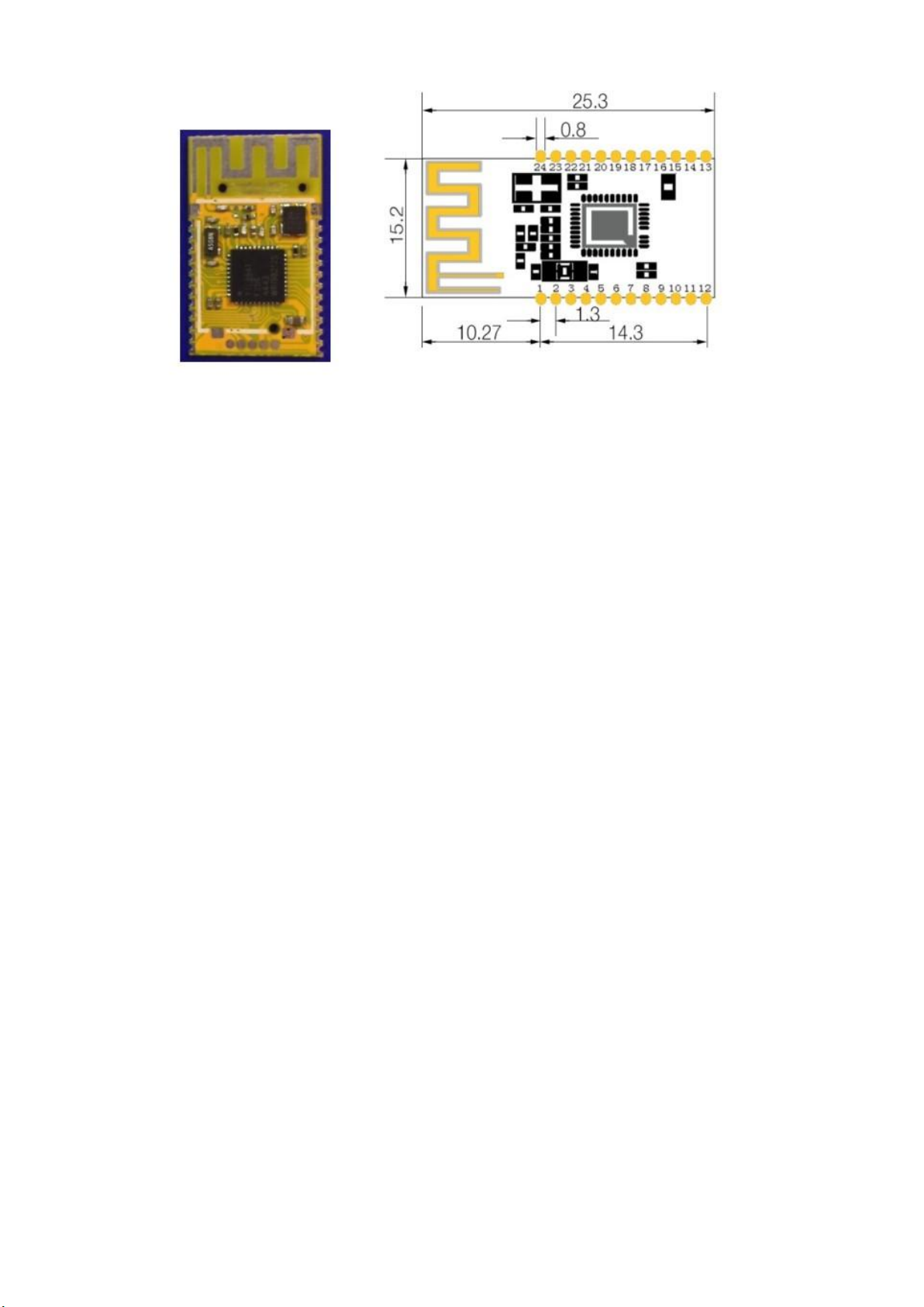
2. WMD410A01SR6A0 (HY-254101) PCBA dimension size and picture
(PCBA dimension size : 15.2*25.3*2.0 mm).
3. Application Note:
3-1.Attention to the electrostatic protection, prevent the soldering iron and the equipment grounding bad;
And the workbench, working environment, packaging materials and from the human body Touch with
static electricity, etc., destroy IC and software be fly; Manual welding module solder iron temperature,
should pay attention to avoid the PCB copper stripping off;Soldering iron strictly Grounding
requirements, eliminating iron power failure module;
3-2.Attention to avoid the overall motherboard power supply circuit of bad welding connected to short
circuit or open circuit, causing the Bluetooth chip, abnormal voltage, The soft ware will fly and
problems of IC was damaged.
3-3.When programming firm ware, the VDDS supply voltage must in DC 2.4~3.3V, To avoid
programming has not completely, and abnormal status occur..
3-4. Use the module in the production and the transport process, please insure module’s component
protection, prevent the precision parts on the module Damaged (welding furnace exit and assembly,
testing, delivery process, suggest using collision buffer material, not collide with each other)
3-5. The module for the humidity sensitive components, if used in SMT reflow soldering operations,
please strictly follow the IPC/JEDECJ - STD – 020 regulation, completes the drying dehumidifying , and
for this module has second processing work after placed in the functional test environment, the humidity
of the chip is no guarantee that in a certain ratio, the honored guest please understand;(The attention note
show in below Fig.)
3-6. The diagram (show in below Fig.) of the module application on external filter parts, when need,
please design in the mainboard, the parts parameter can depend on the actual need to changes.
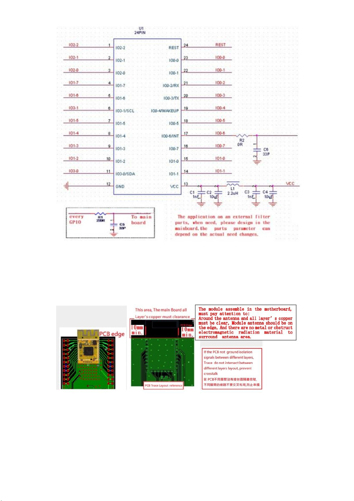
3-7.Assembly recommendation 1:Underneath the module antenna and RF circuit on the main board PCB
copper need to clearance, and place close to the main board edge, as show in below Fig.
The antenna can't be near around metal parts and prevent material existence of electromagnetic radiation,
Can affect the manipulation of the distance.
3-8. Assembly recommendation 2:Signal trace and power supply trace, don't cross layout, as show in below
Fig.To avoid crosstalk, affect the receiving sensitivity.
4. Module pin definition and description of input and output ports
(4-1)HY-254101(PCB Antenna)pin map
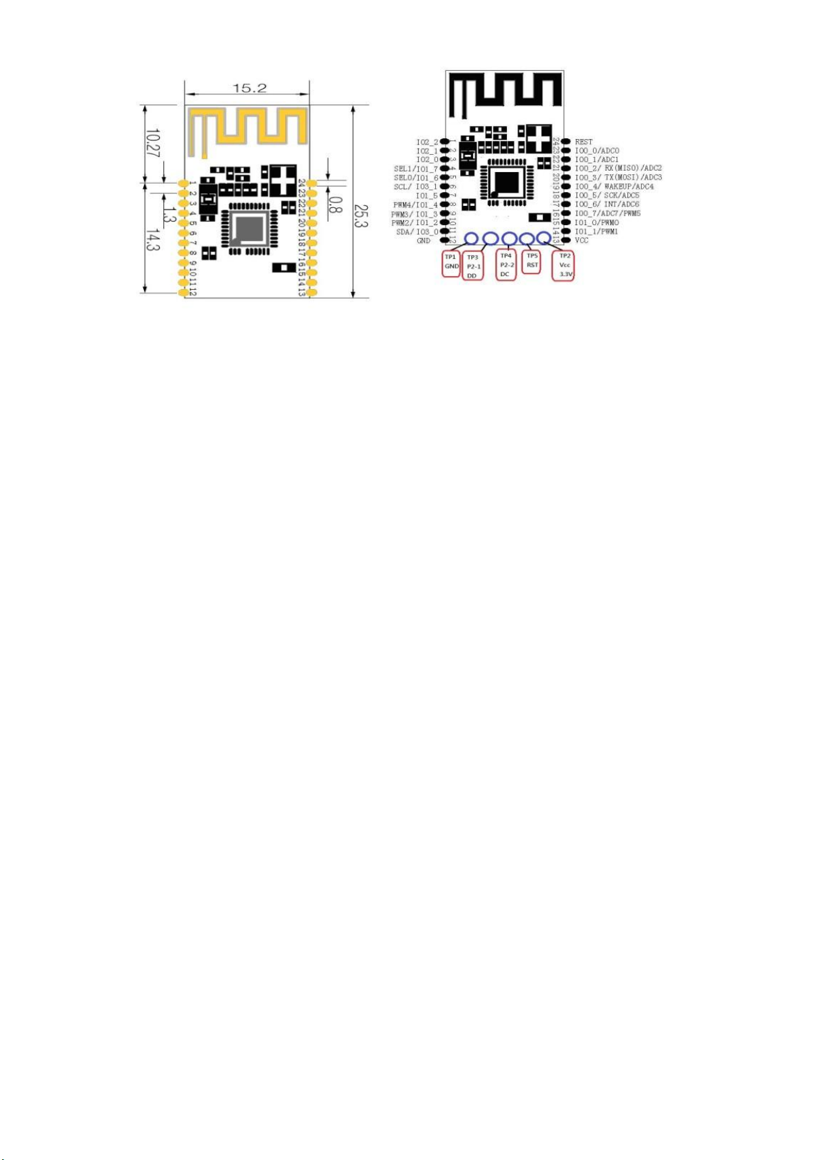
(4-2)Pin function table (Not shown in the I/O pin functions ,Please see
Table(4-3) input and output ports description)
 Loading...