

Page 1

HumDTTM Series
Master Development System
User's Guide
Page 2

Warning: Some customers may want Linx radio frequency (“RF”)
!
products to control machinery or devices remotely, including machinery
or devices that can cause death, bodily injuries, and/or property
damage if improperly or inadvertently triggered, particularly in industrial
settings or other applications implicating life-safety concerns (“Life and
Property Safety Situations”).
NO OEM LINX REMOTE CONTROL OR FUNCTION MODULE
SHOULD EVER BE USED IN LIFE AND PROPERTY SAFETY
SITUATIONS. No OEM Linx Remote Control or Function Module
should be modified for Life and Property Safety Situations. Such
modification cannot provide sufficient safety and will void the product’s
regulatory certification and warranty.
Customers may use our (non-Function) Modules, Antenna and
Connectors as part of other systems in Life Safety Situations, but
only with necessary and industry appropriate redundancies and
in compliance with applicable safety standards, including without
limitation, ANSI and NFPA standards. It is solely the responsibility
of any Linx customer who uses one or more of these products to
incorporate appropriate redundancies and safety standards for the Life
and Property Safety Situation application.
Table of Contents
1 Introduction
2 Ordering Information
2 HumDT
2 HumDT
3 HumDT
3 Programming Dock
3 Programming Dock Objects
4 Prototype Board
4 Prototype Board Objects
5 Initial Setup
6 Using the Prototype Board
8 Using the Programming Dock
10 The Development Kit Demonstration Software
17 Development Kit Demonstration Software Example
TM
Series Transceiver Carrier Board
TM
Series Transceiver Carrier Board Objects
TM
Series Carrier Board Pin Assignments
Do not use this or any Linx product to trigger an action directly
from the data line or RSSI lines without a protocol or encoder/
decoder to validate the data. Without validation, any signal from
another unrelated transmitter in the environment received by the module
could inadvertently trigger the action.
All RF products are susceptible to RF interference that can prevent
communication. RF products without frequency agility or hopping
implemented are more subject to interference. This module does not
have a frequency hopping protocol built in.
Do not use any Linx product over the limits in this data guide.
Excessive voltage or extended operation at the maximum voltage could
cause product failure. Exceeding the reflow temperature profile could
cause product failure which is not immediately evident.
Do not make any physical or electrical modifications to any Linx
product. This will void the warranty and regulatory and UL certifications
and may cause product failure which is not immediately evident.
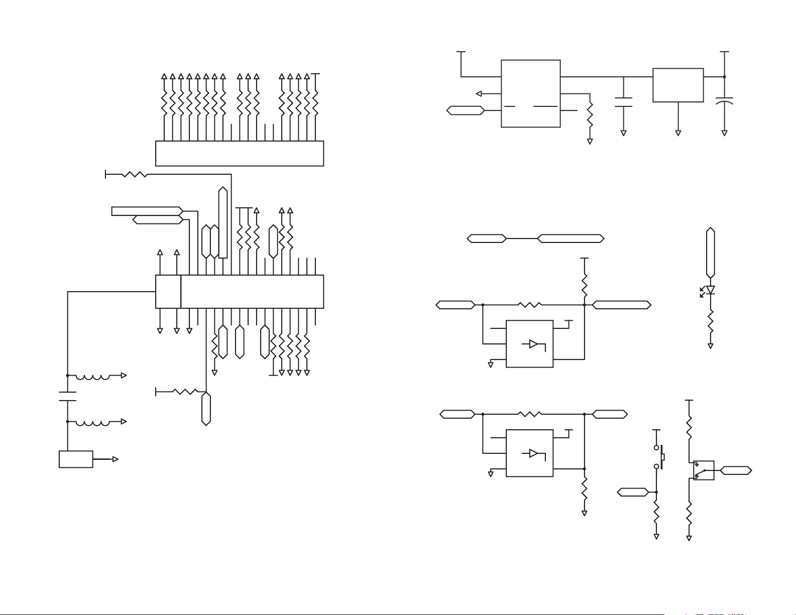
22 Carrier Board Schematic
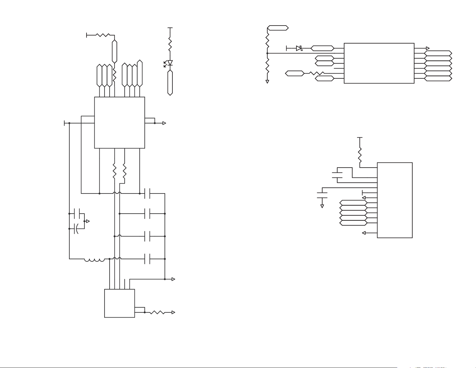
23 Programming Dock Board Schematic
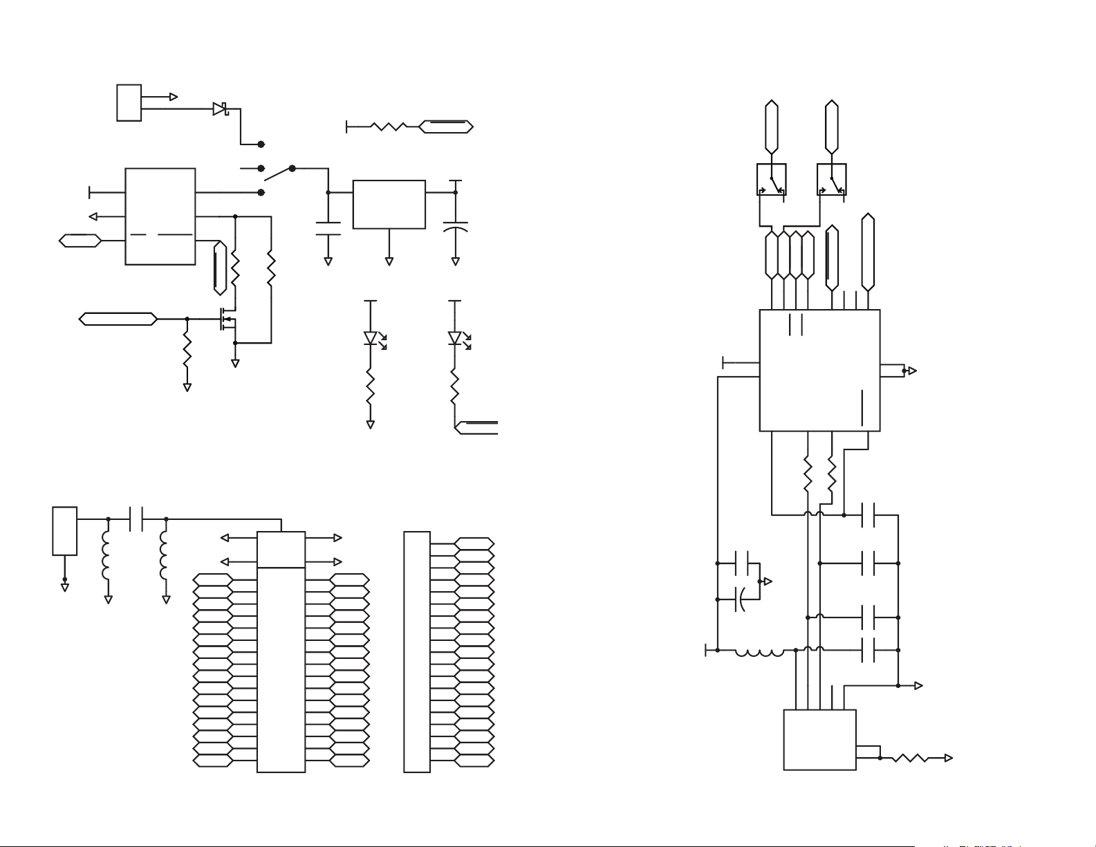
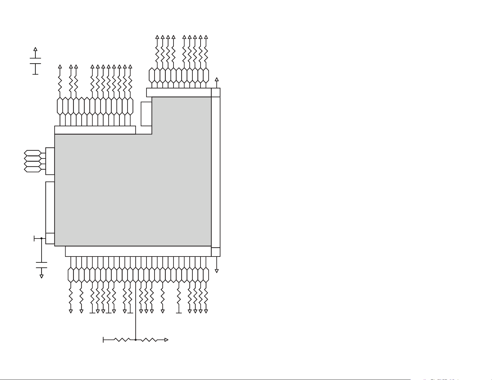
28 Prototype Board Schematic
30 Notes
Page 3
HumDTTM Master Development System
User's Guide
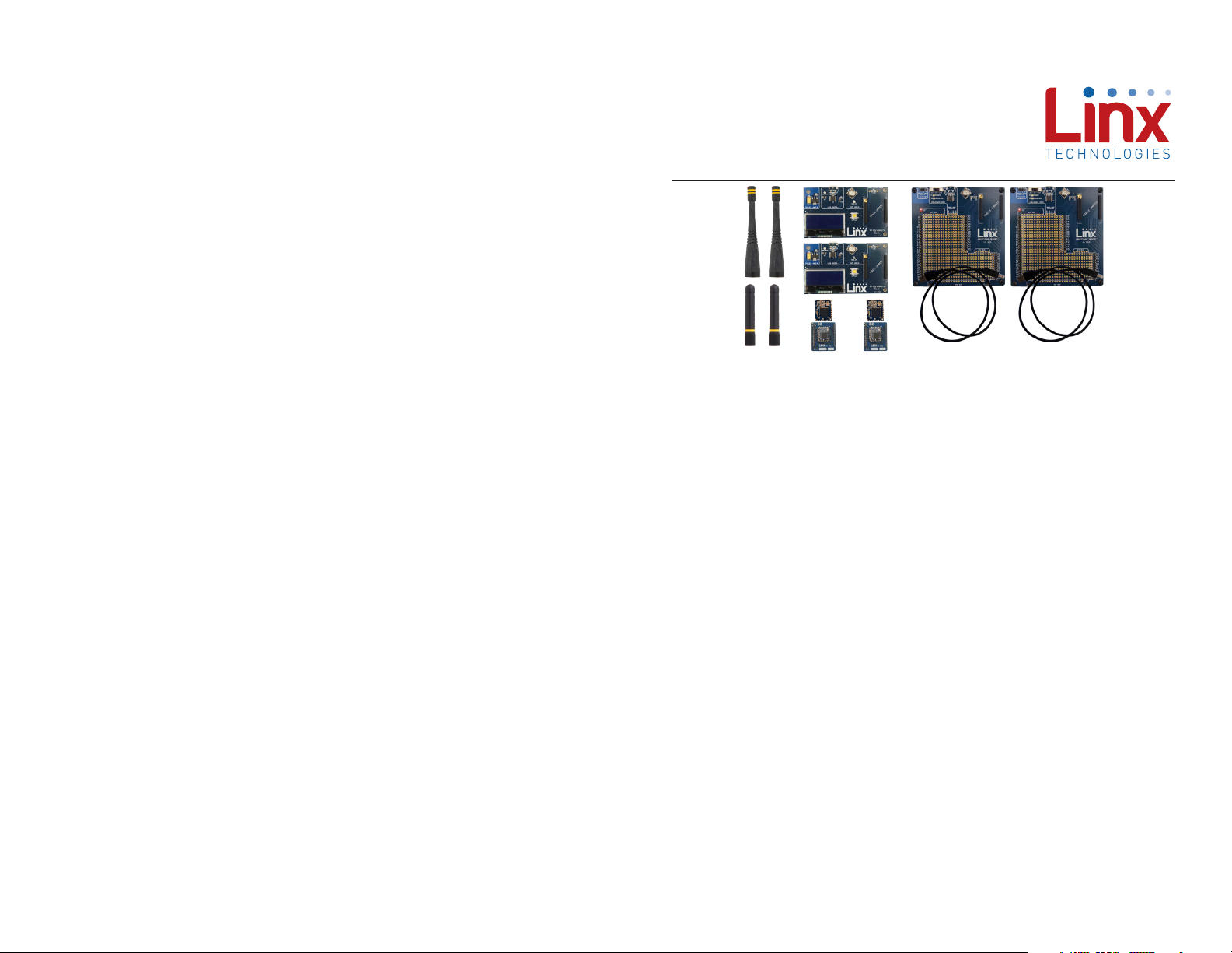
Figure 1: HumDTTM Series Master Development System
Introduction
The Linx HumDTTM Series Remote Control Transceiver modules offer
a simple, efficient and cost-effective method of adding remote control
capabilities to any product. The Master Development System provides a
designer with all the tools necessary to correctly and legally incorporate the
module into an end product. The boards serve several important functions:
• Rapid Module Evaluation: The boards allow the performance of the
Linx HumDT™ Series modules to be evaluated quickly in a user’s
environment. The development boards can be used to evaluate the
range performance of the modules.
• Application Development: A prototyping board allows the development
of custom circuits directly on the board. All signal lines are available on
headers for easy access.
• Software Development: A programming dock with a PC interface allows
development and testing of custom software applications for control of
the module.
• Design Benchmark: The boards provide a known benchmark against
which the performance of a custom design may be judged.
The Master Development System includes 2 Carrier Boards, 2
Programming Dock Boards, 2 Prototype Boards 4 HumDT™ Series
transceivers*, antennas, batteries and full documentation.
* One part is soldered to each Carrier Board
– –
1
Revised 4/23/2015
Page 4
Ordering Information
HumDTTM Series Carrier Board Pin Assignments
Ordering Information
Part Number Description
MDEV-***-DT HumDTTM Series Master Development System
HUM-***-DT HumDTTM Series Transceiver
EVM-***-DT HumDTTM Series Carrier Board
MDEV-PGDCK Development System Programming Dock
MDEV-PROTO Development System Prototype Board
CON-SOC-EVM EVM Module Socket Kit
*** = Frequency; 868MHz, 900MHz
Figure 2: Ordering Information
HumDTTM Series Transceiver Carrier Board
2
ANTENNA 1 2-5 GND (RF Connector)
GND 6
RESET 8
POWER_DOWN 10
NC 12
VCCD 14
LNA_EN 16
GPIO_0 18
PA_EN 20
NC 22
NC 24
NC 26
NC 28
NC 30
NC 32
NC 34
NC 36
7 MODE_IND
9 CMD_DATA_IN
11 VCCD
13 CTS
15 CMD_DATA_OUT
17 VCC
19 VCCD
21 VCCD
23 NC
25 NC
27 NC
29 NC
31 NC
33 NC
35 NC
37 NC
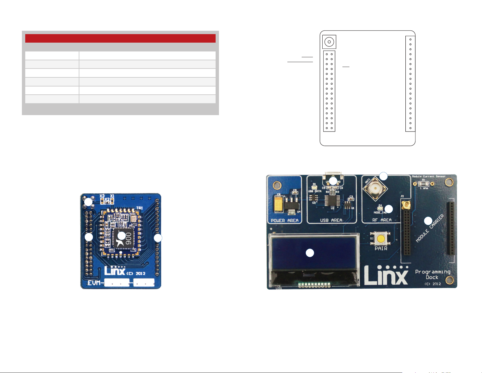
Figure 5: HumDTTM Series Transceiver Carrier Board Pin Assignments (Top View)
Programming Dock
4
2
3
38 VCCD
39 GPIO_7
40 GPIO_6
41 GPIO_5
42 GPIO_4
43 GPIO_3
44 GPIO_2
45 GPIO_1
46 ACTIVE
47 NC
48 NC
49 NC
50 NC
51 NC
52 NC
53 NC
54 NC
55 NC
56 NC
3
1
4
Figure 3: HumDTTM Series Transceiver Carrier Board
HumDTTM Series Transceiver Carrier Board Objects
1. HumDTTM Series Transceiver
2. MMCX RF Connector
3. Dual Row Header
4. Single Row Header
– –
2 3
1
5
Figure 4: Programming Dock
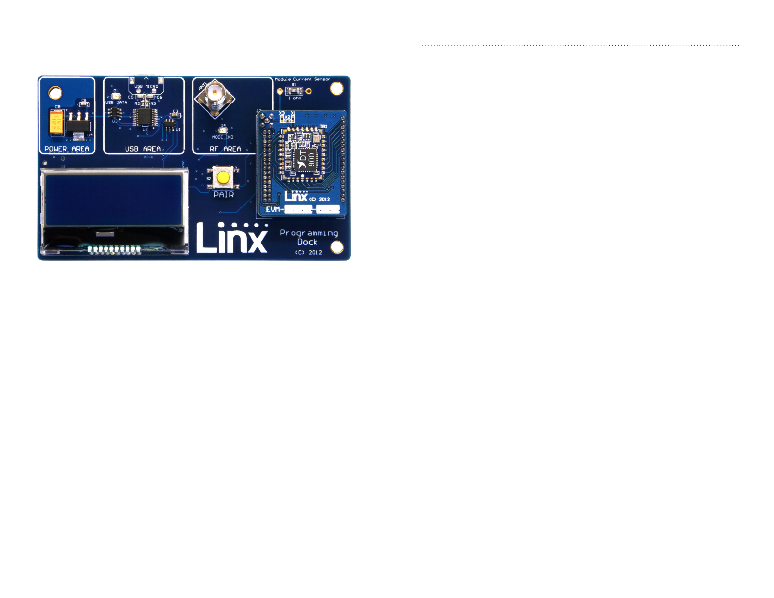
Programming Dock Objects
1. Carrier Board Socket
2. RP-SMA Antenna Connector
3. MODE_IND LED
4. Micro USB Connector
5. LCD Display
– –
Page 5
Prototype Board
6
11
4
5
8
Initial Setup
3
10
7
2
1
11
There are several boards that are included with the Development System.
The Carrier Boards have a HumDTTM Series transceiver on a daughter
board with headers. These boards snap into sockets on the other boards,
enabling the modules to be easily moved among the test boards.
There are two Programming Docks that have a socket for a Carrier
Board and a USB interface for connection to a PC. This is used with the
demonstration software included with the kit to configure the module
through its Command Data Interface.
There are two Prototype Boards that have a socket for a Carrier Board, a
USB interface and a large area of plated through holes that can be used to
develop custom circuitry. The board can be powered either from the USB
connection or an external battery.
11
9
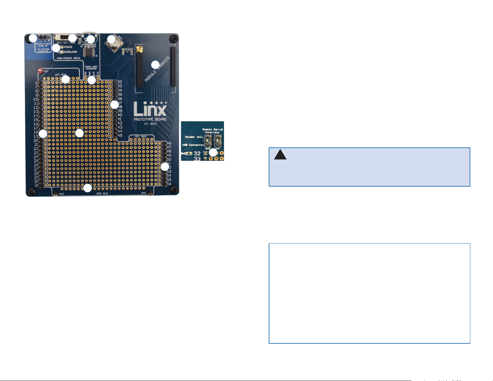
Figure 6: Prototype Board
Prototype Board Objects
1. Carrier Board Socket
2. RP-SMA Antenna Connector
3. Micro USB Connector
4. Power Switch
5. Power LED
6. External Battery Connection
7. Prototyping Area
8. 3.3V Supply Bus
9. Ground Bus
10. USB Interface Lines
11. Module Interface Headers
12. Command Data Interface Routing Switches (on back)
12
Warning: Installing or removing a Carrier Board while power is
!
applied could cause permanent damage to the module. Either turn
off power to the board or unplug the USB cable before installing or
removing a Carrier Board
The development software supports Windows XP, Vista, 7, 8, and 8.1;
OS X 10.6 ‘Snow Leopard’ or later (including Lion, Mountain Lion, and
Mavericks); any version of Linux with Java 1.6 or later.
Note: The Prototype board uses a USB to UART chip to connect the
module to the PC. This chip is powered from the 5V on the USB cable.
It has an input line that detects the voltage on Vcc and sets the UART
voltage levels to match as soon as power is applied to the chip.
It is important that the power switch (SW3) be set appropriately before
the USB cable is plugged in. If an external power supply is used and the
switch is off when the cable is plugged in, then the UART output voltage
may not be set correctly and could result in communication failures.
Set the switch to BAT when using an external supply or to USB to use
the USB bus to power the module. Then plug in the USB cable.
– –
4 5
– –
Page 6
Using the Prototype Board
Snap a Carrier Board onto the socket on the Prototype Board as shown in
Figure 7.
The overload condition is reset once the excess current draw is removed.
Supply for the module is connected through R17. This can be removed and
replaced by another supply or used to measure the current consumption of
the module.
Note: The onboard 3.3-volt regulator has approximately 400mA
available for additional circuitry when plugged into a PC. If more current
is required, the user must power the board from an external supply or a
USB charger with more current capabilities, up to 1A.
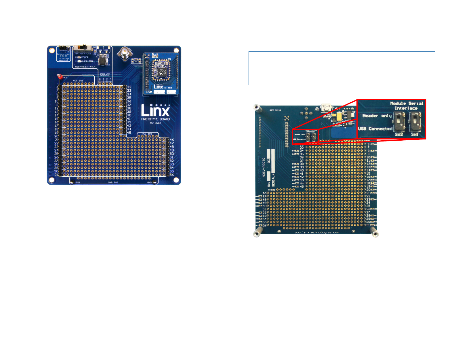
Figure 8 shows the bottom of the board.
Figure 7: Prototype Board with a Carrier Board
Set the power switch (SW3) and connect a micro USB cable into the
connector at the top of the board. Plug the other end into a PC or any
USB charger. The board is powered by the USB bus. This board features
a prototyping area to facilitate the addition of application-specific circuitry.
The prototyping area contains a large area of plated through-holes so that
external circuitry can be placed on the board. The holes are set at 0.100”
on center with a 0.040” diameter, accommodating most industry-standard
SIP and DIP packages.
At the top of the prototyping area is a row connected to the 3.3V power
supply and at the bottom is a row connected to ground. External circuitry
can be interfaced to the transceiver through the breakout headers. The
numbers next to the headers correspond to the pin numbers on the Carrier
Board. Figure 5 shows the pin assignments for the Carrier Board.
The OVERLOAD LED indicates that that too much current is being pulled
from the USB bus. This is used to prevent damage to the parts or the bus.
– –
6 7
Figure 8: Prototype Board Bottom Side
SW1 and SW2 connect the USB interface to the Command Data Interface
lines on the module. This allows the prototype board to be used with the
development kit software or a custom application. When in the “USB
Connected position”, the module is connected to the USB interface. The
“Header Only” position connects the module to the header.
Footprints for 0603 size resistors are on most lines so that pull-ups or
pull-downs can easily be added to the lines. The pads are connected to
VCC or GND based on the most common configuration for the module. The
schematic at the end of this document shows how each line is connected.
– –
Page 7
Using the Programming Dock
Snap a Carrier Board onto the socket on the Programming Dock as shown
in Figure 9.
Figure 9: Programming Dock with a Carrier Board
Connect a micro USB cable into the connector at the top of the board.
Plug the other end into a PC. The board is powered by the USB bus.
The demonstration software included with the kit or custom application
software can be used to configure the module through its Command
Data Interface. The LCD is used to display information about the module.
This includes the module’s local address and a custom nickname. The
nickname is entered using the development kit software and can be
any name that helps distinguish the modules from one another. This is
convenient when multiple programming docks are connected to the same
computer. Please see the development kit software section for more
information on the nicknames.
The HumDTTM Series transceiver has a serial Command Data Interface that
is used to configure and control the transceiver. This interface consists of a
standard UART with a serial command set.
Range Testing
Several complex mathematical models exist for determining path loss in
many environments. These models vary as the transmitter and receiver are
moved from indoor operation to outdoor operation. Although these models
can provide an estimation of range performance in the field, the most
reliable method is to simply perform range tests using the modules in the
intended operational environment.
Range testing can be performed with the Programming Docks and / or
the Prototype Boards. Data can be sent across the link using the included
software or a custom microcontroller connected to the module. The RSSI is
included with the output data messages, so this can be used to qualify the
link.
As the maximum range of the link in the test area is approached, it is not
uncommon for the signal to cut in and out as the radio moves. This is
normal and can result from other interfering sources or fluctuating signal
levels due to multipath effects. This results in cancellation of the transmitted
signal as direct and reflected signals arrive at the receiver at differing times
and phases. The areas in which this occurs are commonly called “nulls”
and simply walking a little farther usually restores the signal. If the signal is
not restored, then the maximum range of the link has been reached.
To achieve maximum range, keep objects such as your hand away from
the antenna and ensure that the antenna on the transmitter has a clear and
unobstructed line-of-sight path to the receiver board. Range performance
is determined by many interdependent factors. If the range you are able to
achieve is significantly less than specified by Linx for the products you are
testing, then there is likely a problem with either the board or the ambient
RF environment in which the board is operating. First, check the battery,
switch positions, and antenna connection. Next, check the ambient RSSI
value with the transmitter turned off to determine if ambient interference
is present. High RSSI readings while the transmitter off indicate there is
interference. If this fails to resolve the issue, please contact Linx technical
support.
– –
8 9
– –
Page 8
The Development Kit Demonstration Software
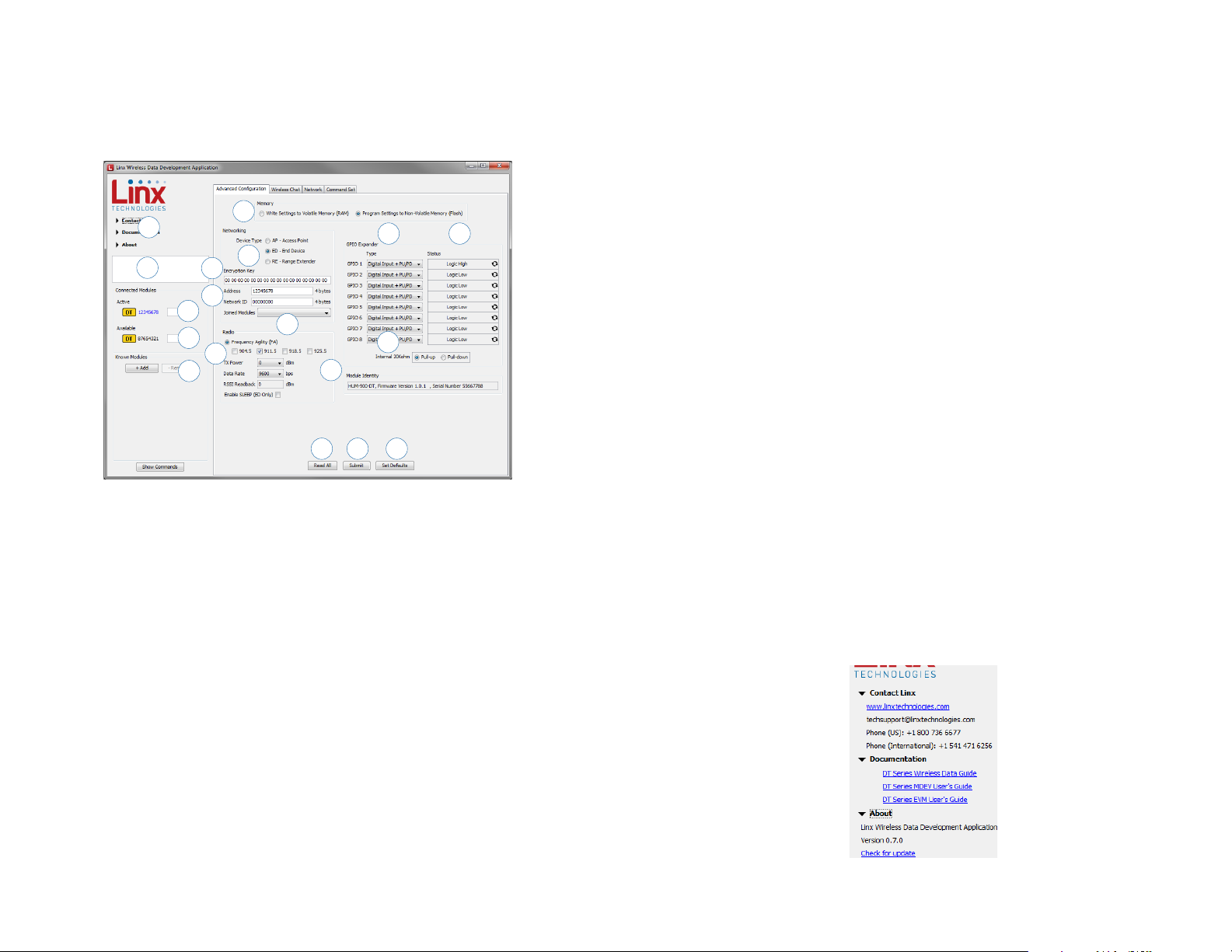
The development kit includes software that is used to configure and control
the module through the Programming Dock. The software defaults to
the Advanced Configuration tab when opened (Figure 10). This window
configures the module’s settings.
6
1
2
3
4
5
Figure 10: The Master Development System Software Advanced Configuration Tab
7
8
9
10
11
15
16 17 18
1. Clicking the Contact Linx, Documentation and About labels on the
left side expands them to show additional information and links to the
latest documentation. This is shown in Figure 11.
2. The Help window shows tips and comments about the software.
3. The active module is connected to the PC and being configured by the
software.
4. Available modules are connected to the PC but are not currently being
configured or controlled by the software.
5. Known Modules are not currently connected to the PC, but have either
been connected to the software in the past or have been manually
entered.
6. The memory setting configures the software to read and write from
either volatile memory or non-volatile memory.
7. The Device Type section configures the module as either an Access
Point, End Device or Range Extender.
8. The Encryption Key box shows the module’s 16 byte AES encryption
12 13
14
key. This can only be read from modules configured as an AP.
9. The Address box shows the module’s current local address. The
Network ID is the identifier of the network that the module is in. No
other module with the same Network ID can have the same Address.
10. The Joined Modules list shows all of the modules that have joined
with the current module. An ED and RE are only joined with an AP, so
they have one entry. An AP can be joined to up to 50 other modules,
including up to 4 REs.
11. The Radio section configures the radio functions. The checkboxes
select which RF channels are used. The TX Power menu sets the
transmitter output power. The data rate menu sets the serial UART
data rate, which the module uses to configure the over-the-air data
rate. The RSSI Readback shows the RSSI value of the last good
packet that was received.
12. The GPIO Expander Type menus configure the eight GPIOs as digital
inputs, digital outputs or analog inputs. The digital inputs are also
configured to use internal pull-up or pull-down resistors, or set to
high-impedance. High impedance deactivates the internal resistors.
13. The Status column shows the current status of all of the GPIO lines on
the active module.
14. The Internal 20kohm radio button sets the internal resistors as either
pull-up or pull-down.
15. The module identity box shows the active module’s name, firmware
version and serial number.
16. The Read All button reads all of the values.
17. The Submit button writes all changes to the active module.
18. The Set Defaults button restores all settings to the factory defaults.
Figure 11: The Master Development System Software Additional Information
– –
10 11
– –
Page 9
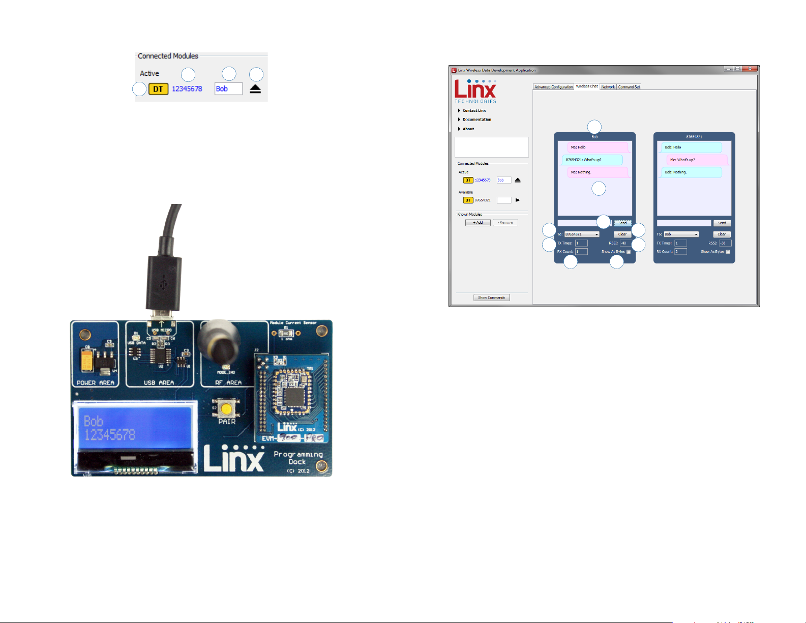
The modules are shown with four identifiers as shown in Figure 12.
3
2
1
Figure 12: The Master Development System Software Module Identifiers
4
1. The type of module (HumDT™ Series)
2. The module’s local address.
3. A custom name that can be given to the module. Type a name into
the box and press Enter to apply it. This name is shown on the LCD
display on the programming dock.
The Wireless Chat tab (Figure 14) offers a demonstration of sending data
between two modules. There is a window for each connected module.
1
2
Figure 13: The Master Development System Programming Dock with Name and Address Displayed
4. The active module has an eject symbol that disconnects the software
from that module when clicked. The Available modules have a play
symbol that makes that module active when clicked.
3
5
6
Figure 14: The Master Development System Software Wireless Chat Tab
74
8
9
1. The top of the window shows the address of the associated module.
2. The chat screen shows the chat messages that have been sent and
received.
3. The Send box is where the message text is entered. The message is
transmitted when the Send button is pressed.
4. The To menu selects the address of the connected module that is to
receive the message (the destination address).
5. The TX Times box shows how many times the module has transmitted.
6. The RX Count box counts the number of messages that the module
has received.
7. The Clear button clears all of the messages from the chat window.
8. The RSSI box indicates the signal strength of the last received
message.
9. When the Show As Bytes box is selected the messages are shown as
bytes in the chat window.
– –
12 13
– –
Page 10
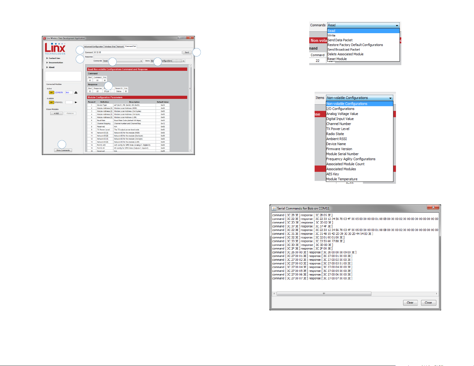
The Command Set tab (Figure 15) allows specific commands to be written
to the module.
1
2
3
4
5
6
7
Figure 15: The Master Development System Software Command Set Tab
1. The Command box shows the hexadecimal values that are written to
the module. Values can be typed into the box or a command can be
selected from the Commands menu.
2. The Response box shows the hexadecimal values that are returned
from the module in response to a command.
3. The Commands drop-down menu shows all of the commands that
are available for the active module (Figure 16). Selecting one of the
commands from this menu automatically fills in the Command box. The
values can be adjusted by typing in the box.
4. The Items drop down menu displays all of the items that are available
for the active module (Figure 17). Selecting one of the items from
this menu automatically fills in the Command box. The values can be
adjusted by typing in the box.
5. Clicking the Send button writes the values in the Command box to the
module.
6. The structure of the selected command and its response is shown in
the main window. Please see the HumDT™ Series Transceiver Data
Guide for definitions of each value.
7. The Show Commands button opens a window that shows all of the
bytes sent to the module and the responses from the module.
Figure 16: The Master Development System Software Command Set Tab Commands Menu
Figure 17: The Master Development System Software Command Set Tab Items Menu
Figure 18: The Master Development System Software Show Commands Window
– –
14 15
– –
Page 11
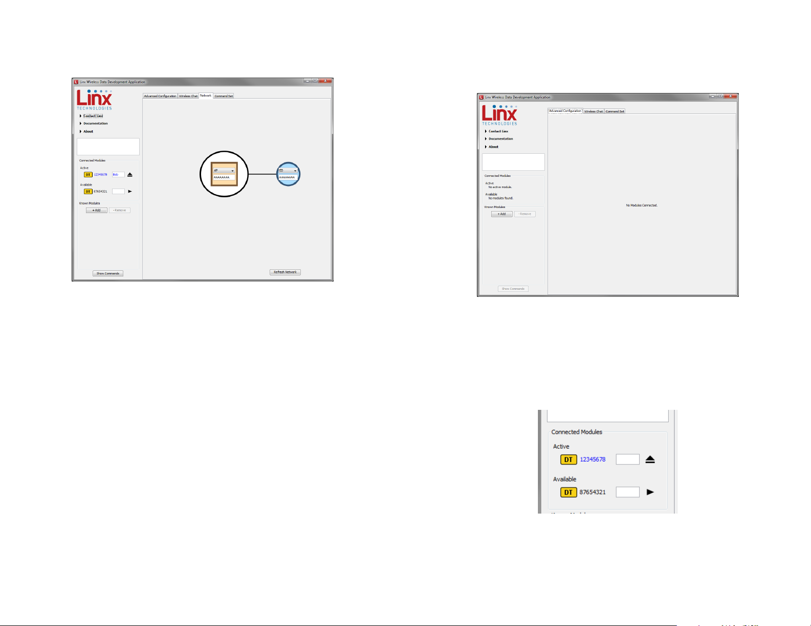
The Network tab shows the interaction of all of the connected modules
on one screen. Figure 19 shows two modules on the screen, but up to 8
modules can fit at one time.
Figure 19: The Master Development System Software Network Tab
The screen shows the network configuration of all modules that are
connected to the PC. The drop-down menu changes the module’s device
type and the text box has the module’s network ID. This screen makes it
easy to quickly set up the network and visually verify its configuration.
Development Kit Demonstration Software Example
This example shows how to configure two modules to work with each
other. The software defaults to the Advanced Configuration tab when
opened (Figure 20).
Figure 20: The Master Development System Software Advanced Configuration Tab at Start-up
Install Carrier Boards onto the Programming Docks and plug a USB cable
between the Programming Docks and the PC. The software automatically
detects attached devices. The first module that is identified appears
under the Active label. This is the module that is actively controlled by
the software. Subsequent modules are listed under the Available label as
shown in Figure 21.
Figure 21: The Master Development System Software Connected Modules
Once the modules are detected by the software, the appropriate options
are displayed on the Advanced Configurations tab and a Network tab
appears. The module’s documents appear under the Documentation link.
– –
16 17
– –
Page 12
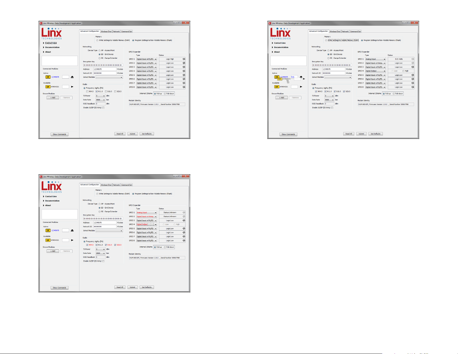
Figure 22: The Master Development System Software with Connected Modules
Figure 24: The Master Development System Software Dragging to Change the Active Module
Any changes to the current configurations are shown in red. These
changes are not written to the module until the Submit button is clicked.
Figure 23: The Master Development System Software Advanced Configuration with Changes
Changing the active module is accomplished by either clicking the play
symbol next to the desired module or dragging it from the Available list to
the Active spot. Changes can now be made to this module.
There are several settings that must match in order for the modules to be
able to communicate. This example uses the following settings.
• The Encryption Key must match on both modules. This can only be
read out of an AP.
• Network ID must match on both devices.
• The UART Baud Rate is 9600.
Other settings can be used as long as they match on both modules. Once
the settings are changed and submitted to both modules, the Network tab
can be used to graphically view the network topology and the Wireless
Chat tab can be used to transfer data.
– –
18 19
– –
Page 13
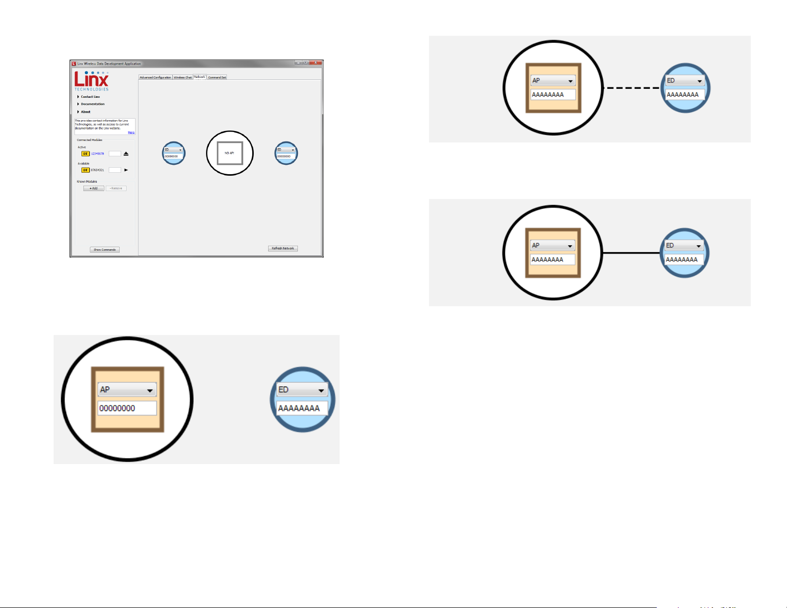
Clicking on the Network tab shows the current state of all modules
connected to the PC.
Figure 25: The Master Development System Software Network Tab
Both modules are set as End Devices. There must be at least one
Access Point in every network, so one module must be changed. This is
accomplished by clicking the drop-down menu on one of the modules and
selecting AP.
Figure 27: The Master Development System Software Network Tab
A dotted line appears between the modules indicating that they are joining
the network.
Figure 28: The Master Development System Software Network Tab
Figure 26: The Master Development System Software Network Tab
Both modules must have the same Network ID, so change the ID number
in one or both of the boxes to match.
– –
20 21
A solid line appears between the modules when they are joined and ready
to communicate. The Wireless Chat tab can now be used to send data
between the modules.
– –
Page 14
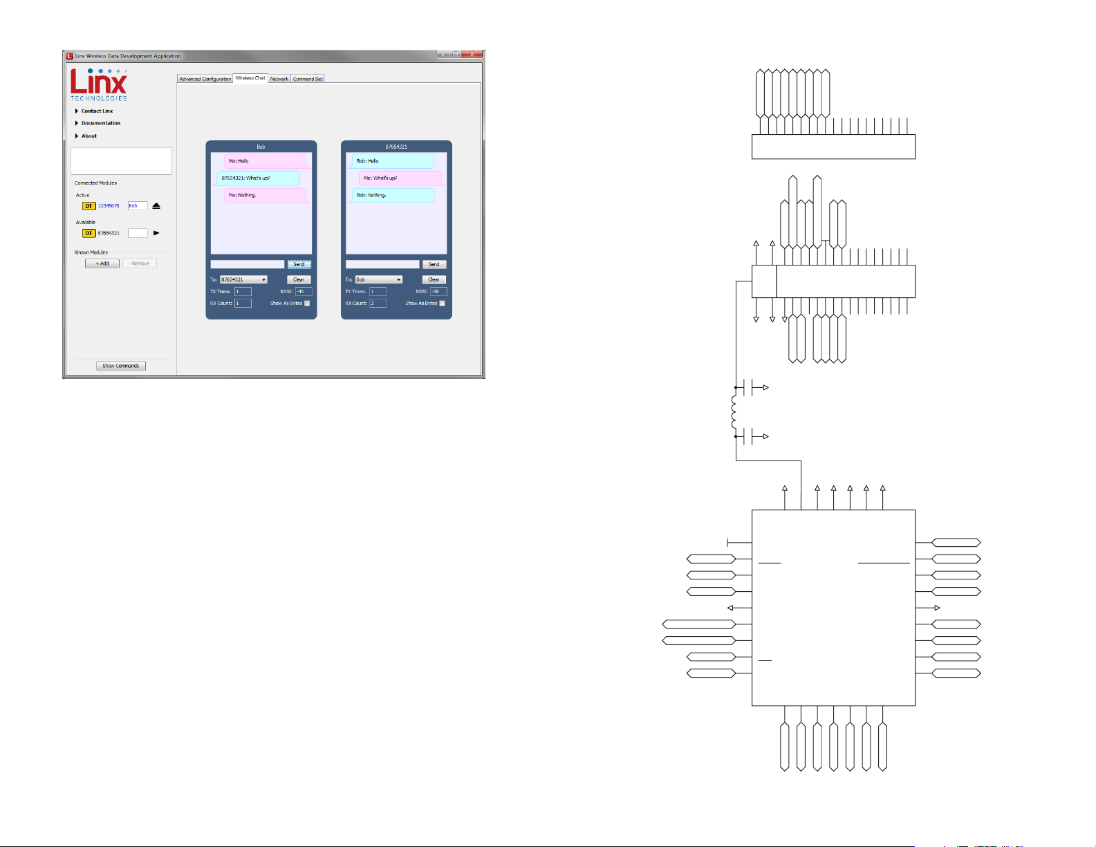
Carrier Board Schematic
Figure 29: The Master Development System Software Wireless Chat Tab
GPIO_5
GPIO_4
GPIO_3
GPIO_2
GPIO_1VCCD5
MODE_IND
VCCD4
CTS
CMD_DATA_IN
CMD_DATA_OUT
67
89
10 11
12 13
14 15
PDN
GND
RESET
GND
GND
19
18
ACTIVE
VCC
16 17
LNA_EN
17
VCCD1
GPIO_7
GPIO_6
38394041424344454647484950515253545556
GND
GND
1
23
45
GND
GND
X3
DNP
GND
X1
1.2pF
X2 5.3nH
GND
20
VCCD3
18 19
20 21
PA_EN
GPIO_0
GND
22 23
GND
24 25
26 27
28 29
30 31
32 33
34 35
36 37
J1
Carrier Interconnect
GND
GND
14
GND
VCC
21
VCC
RESETPDN
LNA_EN
PA_EN
GND
CMD_DATA_OUT
CMD_DATA_IN
CTS
VCCD5
RESET
22
LNA_EN
23
PA_EN
24
GND
25
26
27
CTS
28
VCCD
29
MODE_IND30ACTIVE31GPIO_032GPIO_33GPIO_4
TR1
MODE_IND
Figure 30: HumDTTM Series Transceiver Carrier Board Module Schematic
– –
22 23
ANT
GND
CMD_DATA_OUT
CMD_DATA_IN
1
ACTIVE
GPIO_0
– –
GND
GND16GND15GND
GPIO_1
GPIO_2
2
GPIO_2
GPIO_1 VCCD2
4
GPIO_3
GPIO_4
VCCD
POWER_DOWN
VCCD
VCCD
GND
VCCD
GPIO_7
GPIO_6
GPIO_5
VCCD4
13
21
VCCD3
11
VCCD2
10
9
GND
VCCD1
8
GPIO_7
7
GPIO_6
6
GPIO_5
5
Page 15
GND
GND
GND
GND
GND
GND
GND
GND
GND
GND
GND
GND
GND
GND
GND
VCC
GND
+
C8
100uF
VCC
GND
Vin
1
GND
2
Vout
3
U4
LM3940IMP 3.3V
C9
0.47uF
GND
IN
1
GND
2
EN3FAULT
4
ILIM
5
OUT
6
U3
TPS2552
GND
5VUSB
GND
R11
53.6k
nPWREN
SIGNAL ROUTING
R9 10k
GND
38394041424344454647484950515253545556
GND
GND
GND
GND
GND
GND
GND
GND
GND
GND
GND
GND
GND
R35 10k
R34 10k
R33 10k
R32 10k
R30 10k
R28 10k
R22 10k
R21 10k
R18 10k
R15 10k
R14 10k
R13 10k
R12 10k
R10 10k
GND
R38 10k
VCC
R16
10k
VCC
VCC
R1
1 Ohm
MODE_IND
CMD_DATA_IN
CMD_DATA_OUT
GND
GND
GND GND
GND
1
23
45
67
89
10 11
12 13
14 15
16 17
18 19
20 21
22 23
24 25
26 27
28 29
30 31
32 33
34 35
36 37
J2
Carrier Interconnect
R29 10k
GND
GND
VCC
VCC
R27 10k
R25 10k
R19 10k
R31 10k
VCC
PAIR
GND
R26 10k
GND
R37 10k
GND
R39 10k
GND
R43 10k
R44 10k
GND
R45 10k
GND
RF
1
GND
2-5
ANT1
GND
GND
X1
1nH
X3
DNP
GND
X2
DNP
LADJ
nPDN nCMD
nCTS
GPIO1
GPIO2
Programming Dock Board Schematic
GND
GND
VCC
R1
1 Ohm
R13 10k
R12 10k
R10 10k
38394041424344454647484950515253545556
CMD_DATA_IN
MODE_IND
GND
1
23
45
GND
GND GND
X3
DNP
GND
X1
1
ANT1
RF
1nH
X2
GND
DNP
2-5
VCC
GND
GND
Figure 31: Programming Dock Board RF Carrier Area Schematic
1
2
GND
GND
U3
TPS2552
IN
GND
EN3FAULT
Buffer Bypass DNP
R48 0 ohm
U1
1
2
1
2
VCC
NC
IN
GND3OUT
Buffer Bypass DNP
R49 0 ohm
U5
VCC
NC
IN
GND3OUT
OUT
ILIM
CMD_DATA_OUTRXD
VCC
5
4
VCC
5
4
6
5
4
5VUSB
VCC
GND
R22 10k
R21 10k
R18 10k
R15 10k
R14 10k
CMD_DATA_OUT
nCTS
67
89
10 11
12 13
14 15
GND
R16
10k
– –
24 25
PAIR
R19 10k
GND
nPDN nCMD
R9 10k
R25 10k
16 17
GND
GND
VCC
VCC
R27 10k
18 19
20 21
LADJ
R28 10k
R29 10k
GND
R30 10k
GND
22 23
GPIO1
24 25
26 27
GPIO2
VCC
GND
GND
GND
GND
GND
GND
R32 10k
GND
R44 10k
28 29
R31 10k
GND
GND
R33 10k
GND
30 31
R26 10k
GND
GND
R35 10k
R34 10k
R45 10k
32 33
R37 10k
R39 10k
GND
GND
R38 10k
34 35
R43 10k
GND
36 37
J2
Carrier Interconnect
GND
nPWREN
Figure 32: Programming Dock Board Power Supply Area Schematic
RTS nCMD
Figure 33: Programming Dock Board Signal Routing Schematic
R11
53.6k
R46
10k
R17
10k
CMD_DATA_INTXD
GND
GND
VCC
GND
– –
C9
0.47uF
PAIR
U4
LM3940IMP 3.3V
1
Vin
GND
VCC
S2
PAIR
R24
10k
GND
VCC
3
Vout
D4
GND
R40
0 ohm
SW1
R41
0 ohm
+
GND
MODE_IND
R8
330 ohm
GND
2
VCC
GND
C8
100uF
MODE_IND BLUE
LADJ
Page 16
USB AREA POWER SUPPLY AREA RF MODULE CARRIER AREA
MICROCONTROLLER AREA
GND
+
C1
C6
47pF
C2
0.1uF
VCC
12
VCCIO
3
3V3OUT
10
GND
5
GND
13
USBDM9USBDP8RESET#
11
TXD
1
RXD
4
RTS#2CTS#
6
CBUS015CBUS114CBUS27CBUS3
16
U2
FT230X
C5
47pF
nPWREN
C7
0.1uF
GND
5VUSB
RTS
R2 27
R3 27
TXD
RXD
nCTS
VCC
R20
10k
R47 0 ohm
GPIO2
RXTX LED
D1
R5
330 ohm
ORANGE
RXTX LED
VCC
GPIO1
GND
+
C8
100uF
VCC
GND
Vin
1
GND
2
Vout
3
U4
LM3940IMP 3.3V
C9
0.47uF
GND
IN
1
GND
2
EN3FAULT
4
ILIM
5
OUT
6
U3
TPS2552
GND
5VUSB
GND
R11
53.6k
nPWREN
USB AREA POWER SUPPLY AREA RF MODULE CARRIER AREA
SIGNAL ROUTING
R20
R17
10k
GND
NC
1
IN
2
GND3OUT
4
VCC
5
U5
VCC
GND
R49 0 ohm
Buffer Bypass DNP
RTS nCMD
CMD_DATA_OUTRXD
NC
1
IN
2
GND3OUT
4
VCC
5
U1
VCC
GND
R46
10k
VCC
R48 0 ohm
CMD_DATA_INTXD
Buffer Bypass DNP
GND
MODE_IND
R8
330 ohm
D4
MODE_IND BLUE
R24
10k
S2
VCC
PAIR
PAIR
R41
0 ohm
R40
0 ohm
VCC
SW1
LADJ
10k
VCC
RTS
TXD
RXD
1
4
6
TXD
RXD
RTS#2CTS#
3
12
5VUSB
VCCIO
VCC
3V3OUT
U2
FT230X
10
R2 27
C2
0.1uF
4.7uF
GND
L1
600R/1.3A
1
J1
Micro USB
2
5V
+
C1
Figure 34: Programming Dock Board USB Area Schematic
– –
nCTS
nPWREN
R47 0 ohm
CBUS015CBUS114CBUS27CBUS3
GPIO2
GPIO1
16
RXTX LED
GND
13
GND
5
ORANGE
VCC
GND
R5
330 ohm
D1
RXTX LED
nPDN
R36
DNP
VCC GND
R23
DNP
GND
D2
RXD
VCCP
GPIO1
PGM
R42 DNP
CSB RS
1
2
3
4
5
6
7
U8
VDC
RA5
RA4
MCLR
RC5
RC4
RC3
PIC16F1825-I/ST
USBDM9USBDP8RESET#
11
R3 27
C7
0.1uF
C6
47pF
C5
3NC4
DAT+
DAT-
5
GND
GSHD
GSHD
47pF
Figure 35: Programming Dock Board Microcontroller Area Schematic
C4
0.01uF
6
R4
0
7
GND
GND
26 27
GND
C14
1uF
C13
1uF
SI
SCL
CSB
RS
RST
VCC
GND
GND
– –
VCC
R6
0 Ohm
1
2
3
4
5
6
7
8
9
10
11
12
LCD1
2x16 LCD
LED+
C1C1+
VOUT
VCC
GND
SI
SCL
CSB
RS
RST
LED-
ICSPDAT
ICSPCLK
GND
RA2
RC0
RC1
RC2
14
13
PGD
12
PGC
11
RST
10
SCL
9
SI
8
Page 17
GND
R24
330
5VUSB
D2
POWER (GREEN)
D3
OVER CURRENT (RED)
R22
330
VCC
FAULT
U2
R5
10k
GND
5VUSB
GND
+
C7
100uF
VCC
GND
Vin
1
GND
2
Vout
3
U3
C8
0.47uF
GND
FAULT
IN
1
GND
2
EN3FAULT
4
ILIM
5
OUT
6
TPS2553
SW3
5VUSB
EN
FAULT
GND1
2
J3
100mil Header
Battery Input
D1
USB AREA POWER SUPPLY AREA
RF MODULE CARRIER AREA
GND
R7
53.6kR953.6k
GND
Q1
R3
10k
BCD Charger
RF
1
23
45
67
89
10 11
12 13
14 15
16 17
18 19
20 21
22 23
24 25
26 27
28 29
30 31
32 33
34 35
36 37
38
39
40
41
42
43
44
45
46
47
48
49
50
51
52
53
54
55
56
J2
Carrier Interconnect Female
1
GND
2-5
ANT1
CONREVSMA001
GND
GND
GND
GND
GND
7
89
10 11
12 13
14 15
16 17
18 19
20 21
22 23
24 25
26 27
28 29
30 31
32 33
34 35
36 37
38
39
40
41
42
43
44
45
46
47
48
49
50
51
52
53
54
55
56
X1
0 Ohm
6
X3
DNP
GND
GND
X2
DNP
FAULT
GND BUS
1
TP3
39404142434445
4647484950515253545556
38
37
36
35
323334
1
2
3
4
J6
100mil Header
TXD
RXD
RTS
CTS
VCC BUS
123456789
10
11
J7 100mil Header
123456789
1011121314
J4
100mil Header
R45DNP
GND
R44DNP
R43DNP
R42DNP
R41DNP
R40DNP
R39DNP
R38DNP
GND
GND
GND
GND
GND
GND
GND
GND
R52DNP
R50DNP
GND
R47DNP
GND
R48DNP
GND
R49DNP
GND
PROTOTYPE AREA
C10
0.1uF
GNDVCC
R32 DNP
GND
R34 DNP
GND
R35 DNP
GND
R53 DNP
GND
R54 DNP
GND
R55 DNP
GND
R56 DNP
GND
GND
R24
330
5VUSB
D2
POWER (GREEN)
D3
OVER CURRENT (RED)
R22
330
VCC
FAULT
VCC BUS
GND BUS
1
TP3
1
TP2
GND GND
1
TP4
VCC
39404142434445
4647484950515253545556
38
37
36
35
293031
323334
789101112131415161718192021222324252627
28
1
2
3
4
J6
100mil Header
TXD
RXD
RTS
CTS
12345678910111213141516171819202122232425
26
J5
100mil Header
VCC BUS
6
R6 0
GND
VCC
R10 DNP
VCC
123456789
10
11
J7 100mil Header
123456789
1011121314
J4
100mil Header
R45DNP
GND
R44DNP
R43DNP
R42DNP
R41DNP
R40DNP
R39DNP
R38DNP
GND
GND
GND
GND
GND
GND
GND
GND
R52DNP
R19 DNP
GND
VCC
R11 DNP
GND
R50DNP
GND
R14 DNP
GND
R170
VCC
R12 DNP
GND
R26 DNP
R23 DNP
GND
R21 DNP
GND
R47DNP
GND
R48DNP
GND
R49DNP
GND
R15
DNP
VCC
R18
DNP
GND
R13 DNP
U2
R5
10k
GND
5VUSB
GND
+
C7
100uF
VCC
GND
Vin
1
GND
2
Vout
3
U3
C8
0.47uF
GND
FAULT
IN
1
GND
2
EN3FAULT
4
ILIM
5
OUT
6
TPS2553
SW3
EN
FAULT
GND1
2
J3
100mil Header
Battery Input
D1
RF MODULE CARRIER AREA
PROTOTYPE AREA
PROTOTYPE AREA
GND
R7
53.6kR953.6k
GND
Q1
R3
10k
BCD Charger
C10
0.1uF
GNDVCC
R8 DNP
GND
R16 DNP
GND
R20 DNP
GND
R28 DNP
GND
R29 DNP
VCC
R30 DNP
GND
R31 DNP
GND
C9
0.1uF
GND
R32 DNP
GND
R34 DNP
GND
R35 DNP
GND
R53 DNP
GND
R54 DNP
GND
R55 DNP
GND
R56 DNP
GND
Prototype Board Schematic
J3
GND1
OUT
ILIM
GND
X3
DNP
GND
2
100mil Header
Battery Input
U2
1
IN
2
GND
EN3FAULT
TPS2553
BCD Charger
5VUSB
GND
EN
Figure 36: Prototype Board Power Supply Area Schematic
CONREVSMA001
ANT1
1
RF
GND
2-5
GND
X1
0 Ohm
X2
DNP
GND
Figure 37: Prototype Board RF Carrier Area Schematic
D1
SW3
6
5
4
R3
10k
GND
GND
6
89
10 11
12 13
14 15
16 17
18 19
20 21
22 23
24 25
26 27
28 29
30 31
32 33
34 35
36 37
R7
53.6kR953.6k
FAULT
Q1
GND
23
45
67
89
10 11
12 13
14 15
16 17
18 19
20 21
22 23
24 25
26 27
28 29
30 31
32 33
34 35
36 37
– –
5VUSB
C8
0.47uF
GND
J2
Carrier Interconnect Female
1
28 29
R5
10k
U3
1
Vin
GND
VCC
D2
R22
330
POWER (GREEN)
GND
GND
GND
7
FAULT
VCC
3
Vout
GND
2
+
C7
100uF
GND
5VUSB
38
39
40
41
42
43
44
45
46
47
48
49
50
51
52
53
54
55
56
R24
330
OVER CURRENT (RED)
38
39
40
41
42
43
44
45
46
47
48
49
50
51
52
53
54
55
56
D3
Figure 38: Prototype Board USB Area Schematic
9
CMD_DATA_IN
SW1
VCC
TXD
1
TXD
3
12
3V3OUT
U6
10
4
CMD_DATA_OUT
SW2
RXD
RTS
CTS
6
2
CTS
RTS
RXD
VCCIO
VCC
USBDM9USBDP8RESET
R1 27
R2 27
C2
0.1uF
5VUSB
+
C1
4.7uF
L1
600R/1.3A
GND
1
2
3NC4
5V
DAT+
DAT-
J1 Micro USB
– –
15
PWREN#
BCD Charger
16
CBUS015CBUS114CBUS27CBUS3
GND
GND
11
C6
0.1uF
C5
C4
C3
5
GND
GSHD
6
GSHD
7
FT230X
13
5
GND
47pF
47pF
0.01uF
GND
R4
0
GND
Page 18
TP3
PROTOTYPE AREA
C10
GNDVCC
CTS
RTS
RXD
TXD
GND
0.1uF
R32 DNP
R34 DNP
323334
123456789
J4
100mil Header
4
3
2
1
J6
100mil Header
Notes
GND
GND
GND
GND
GND
GND
GND
GND
R53 DNP
R52DNP
R48DNP
R49DNP
R50DNP
GND
GND
R35 DNP
R38DNP
37
36
35
GND
GND
GND
GND
R41DNP
R40DNP
R39DNP
39404142434445
38
1011121314
R42DNP
GND
GND
GND
GND
R45DNP
R44DNP
R43DNP
R47DNP
4647484950515253545556
123456789
J7 100mil Header
VCC BUS
GND
R54 DNP
R55 DNP
R56 DNP
1
10
11
GND BUS
VCC BUS
0.1uF
1
VCC
TP4
C9
GND
12345678910111213141516171819202122232425
J5
100mil Header
789101112131415161718192021222324252627
6
R8 DNP
R6 0
R10 DNP
R11 DNP
R12 DNP
R13 DNP
VCC
GND
GND
VCC
GND
GND
VCC
Figure 39: Prototype Board Prototype Area Schematic
PROTOTYPE AREA
1
26
TP2
293031
28
GND GND
R16 DNP
R14 DNP
GND
R15
DNP
– –
30 31
R170
GND
R20 DNP
R19 DNP
VCC
GND
GND
R18
R21 DNP
GND
DNP
R23 DNP
GND
GND
R26 DNP
VCC
R28 DNP
GND
R29 DNP
VCC
R30 DNP
GND
R31 DNP
GND
– –
Page 19

Linx Technologies
159 Ort Lane
Merlin, OR, US 97532
Phone: +1 541 471 6256
Fax: +1 541 471 6251
www.linxtechnologies.com
Disclaimer
Linx Technologies is continually striving to improve the quality and function of its products. For this reason, we
reserve the right to make changes to our products without notice. The information contained in this Data Guide
is believed to be accurate as of the time of publication. Specifications are based on representative lot samples.
Values may vary from lot-to-lot and are not guaranteed. “Typical” parameters can and do vary over lots and
application. Linx Technologies makes no guarantee, warranty, or representation regarding the suitability of any
product for use in any specific application. It is the customer’s responsibility to verify the suitability of the part for
the intended application. NO LINX PRODUCT IS INTENDED FOR USE IN ANY APPLICATION WHERE THE SAFETY
OF LIFE OR PROPERTY IS AT RISK.
Linx Technologies DISCLAIMS ALL WARRANTIES OF MERCHANTABILITY AND FITNESS FOR A PARTICULAR
PURPOSE. IN NO EVENT SHALL LINX TECHNOLOGIES BE LIABLE FOR ANY OF CUSTOMER’S INCIDENTAL OR
CONSEQUENTIAL DAMAGES ARISING IN ANY WAY FROM ANY DEFECTIVE OR NON-CONFORMING PRODUCTS
OR FOR ANY OTHER BREACH OF CONTRACT BY LINX TECHNOLOGIES. The limitations on Linx Technologies’
liability are applicable to any and all claims or theories of recovery asserted by Customer, including, without
limitation, breach of contract, breach of warranty, strict liability, or negligence. Customer assumes all liability
(including, without limitation, liability for injury to person or property, economic loss, or business interruption) for
all claims, including claims from third parties, arising from the use of the Products. The Customer will indemnify,
defend, protect, and hold harmless Linx Technologies and its officers, employees, subsidiaries, affiliates,
distributors, and representatives from and against all claims, damages, actions, suits, proceedings, demands,
assessments, adjustments, costs, and expenses incurred by Linx Technologies as a result of or arising from any
Products sold by Linx Technologies to Customer. Under no conditions will Linx Technologies be responsible for
losses arising from the use or failure of the device in any application, other than the repair, replacement, or refund
limited to the original product purchase price. Devices described in this publication may contain proprietary,
patented, or copyrighted techniques, components, or materials. Under no circumstances shall any user be
conveyed any license or right to the use or ownership of such items.
©2015 Linx Technologies. All rights reserved.
The stylized Linx logo, Wireless Made Simple, WiSE, CipherLinx and the stylized CL logo are trademarks of Linx Technologies.
 Loading...