

Page 1

F4 Series
Evaluation Module
User's Guide
Page 2

Warning: Some customers may want Linx radio frequency (“RF”)
!
products to control machinery or devices remotely, including machinery
or devices that can cause death, bodily injuries, and/or property
damage if improperly or inadvertently triggered, particularly in industrial
settings or other applications implicating life-safety concerns (“Life and
Property Safety Situations”).
Table of Contents
1 Description
2 Ordering Information
2 ElectricalSpecications
NO OEM LINX REMOTE CONTROL OR FUNCTION MODULE
SHOULD EVER BE USED IN LIFE AND PROPERTY SAFETY
SITUATIONS. No OEM Linx Remote Control or Function Module
should be modified for Life and Property Safety Situations. Such
modification cannot provide sufficient safety and will void the product’s
regulatory certification and warranty.
Customers may use our (non-Function) Modules, Antenna and
Connectors as part of other systems in Life Safety Situations, but
only with necessary and industry appropriate redundancies and
in compliance with applicable safety standards, including without
limitation, ANSI and NFPA standards. It is solely the responsibility
of any Linx customer who uses one or more of these products to
incorporate appropriate redundancies and safety standards for the Life
and Property Safety Situation application.
Do not use this or any Linx product to trigger an action directly
from the data line or RSSI lines without a protocol or encoder/
decoder to validate the data. Without validation, any signal from
another unrelated transmitter in the environment received by the module
could inadvertently trigger the action.
All RF products are susceptible to RF interference that can prevent
communication. RF products without frequency agility or hopping
implemented are more subject to interference. This module does not
have a frequency hopping protocol built in.
3 Pin Assignments
3 Pin Descriptions
4 Schematic
5 PCB Layout
5 Power Supply Requirements
Do not use any Linx product over the limits in this data guide.
Excessive voltage or extended operation at the maximum voltage could
cause product failure. Exceeding the reflow temperature profile could
cause product failure which is not immediately evident.
Do not make any physical or electrical modifications to any Linx
product. This will void the warranty and regulatory and UL certifications
and may cause product failure which is not immediately evident.
Page 3
F4 Series GPS Receiver
Evaluation Module
User's Guide
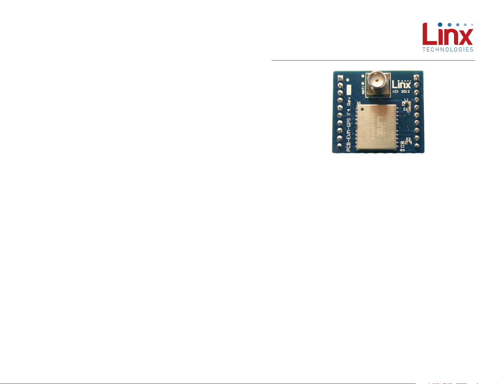
Figure 1: F4 Series Evaluation Module
Description
The F4 Series GPS receiver module is a self-contained high-performance
GPS receiver with an on-board LNA and SAW filter. Based on the SiRFstar
IV chipset, it provides exceptional sensitivity, even in dense foliage
and urban canyons. The module’s very low power consumption helps
maximize runtimes in battery powered applications. With over 200,000
effective correlators, the F4 Series receiver can acquire and track up to 48
satellites simultaneously in just seconds, even at the lowest signal levels.
These features, along with the module’s standard NMEA data output,
make it easy to integrate, even by engineers without previous RF or GPS
experience. The Linx F4 Series GPS modules offer a simple, efficient and
costeffective method of adding GPS capabilities to any product.
The evaluation module contains the surface mount F4 Series GPS module,
an SMA connector, a 1.8V regulator, voltage level shifters (voltage level
protection for RXM and TXM lines), a microcontroller (performs F4 power
up sequence), a power source switch (switches to VBACKUP when VCC
is removed) and a ferrite bead (used to supply power to an external active
antenna, such as the Linx SH Series active GPS antenna), all on a single
board with through-hole headers. This small board makes prototyping with
the F4 Series module very easy.
– –
1
Revised 3/18/2015
Page 4
Ordering Information
Pin Assignments
Ordering Information
Part Number Description
EVM-GPS-F4 F4 Series Evaluation Module
RXM-GPS-F4 F4 Series GPS Receiver Module
Figure 2: Ordering Information
ElectricalSpecications
Ordering Information
Parameter Designation Min. Typ. Max. Units Notes
POWER SUPPLY
Supply Voltage V
Input Pin Voltage 3.6 VDC
Output Pin Voltage 1.8 VDC
Supply Current I
Peak 130 mA 1
Acquisition 46 mA 1
Tracking 27.5 mA 1
Hibernate 20 µA 2
Ready-to-Start 9 µA 2
ANTENNA PORT
RF Input Impedance R
ENVIRONMENTAL
Operating Temperature Range –30 +85 °C
Storage Temperature Range –40 +85 °C
Notes:
1. VCC = 1.8V
2. Initial state after power us applied
Figure 3: Electrical Specifications
CC
CC
IN
Warning: This product incorporates numerous static-sensitive
components. Always wear an ESD wrist strap and observe proper ESD
handling procedures when working with this device. Failure to observe
this precaution may result in module damage or failure.
1.71 1.8 1.89 VDC
50 Ω
GND
GPIOD
GPIOE
TXM
RXM
1PPS
RESET
RFPWRUP
ON_OFF
GND
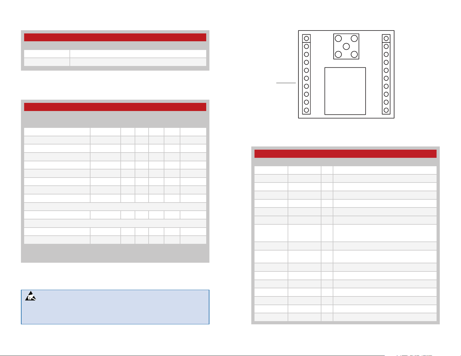
Figure 4: EVM-GPS-F4 Pin Assignments
Pin Descriptions
Pin Descriptions
Pin Number Name I/O Description
1 GPIOD I/O General Purpose I/O. 3.6V tolerant.
2 GPIOE I/O General Purpose I/O. 3.6V tolerant.
3 1PPS O 1 Pulse Per Second. 1.8V level.
4 TX O Serial output (default NMEA)
5 RX I Serial input (default NMEA). 3.6V tolerant.
6 GPIOC I/O General Purpose I/O. 3.6V tolerant.
7, 11 P1, P2 I Pull to 1.8V VCC through 2.2k resistors.
8 /RESET I
9 RFPWRUP O Power State Indicator
10 ON_OFF I
12 VCC P Supply Voltage
13 G1 I Pull to GND through a 100k resistor.
14 GPIOA I/O General Purpose I/O. 3.6V tolerant.
15 GPIOB I/O General Purpose I/O. 3.6V tolerant.
16, 17 NC − No electrical connection.
18, 20, 21, 22 GND P Ground
19 RFIN I GPS RF signal input
Reset Input. Active low with an internal pull-up.
Internal reset is preferred; external reset will clear all
RAM. 3.6V tolerant.
Power Control Pin. Internal 10k pull-down resistor.
3.6V tolerant.
GND
NC
NC
VCC
NC
VBACKUP
GPIOC
GPIOB
GPIOA
GND
Figure 5: F4 Series GPS Receiver Pin Descriptions
– –
2 3
– –
Page 5
Schematic
1.20”
(2.54)
ANT1
PCB Layout
GND
2-5
RF
1
CONSMA001
GND
(47.24)
Ø0.04” x 10
(1.02)
U4
VCCNC
5
VCC
1IN2
V1.8
U3
U6
TXM
2
1
4,7
TX_SHIFT
4
OUT
GND
MC74VHC1GT50
3
GND
C3
1uF
Vout
GND
Vin
C2
1uF
VCC
5S63,8
C
G
A1NC2D
VCC
V1.8NC
5
VCC
U5
1IN2
J3
GND
3
GND
GND
FDFMA2P857
VBACKUP
RX_SHIFT
1
VPP MCLR
4
OUT
GND
3
GND RXM
PGC
4
5NC6
PGC
VDD2GND
3
VPRG
MC74VHC1GT50
PGD
PGD
GND
Program Header
L1
300ohm BEAD
VCC
C1
18pF
GND
20
U1
123456789
J2
VCC
GND
123456789
J1
GND
GPIOE
GPIOD
TX_SHIFT
V1.8
GND
17
10
10
GND GND
GND
GPIOA
GPIOBGPIOC
15
22
NC16NC
GND
GPIOA14GPIOB
GND
21
TXM
RXM
GND
R2
V1.8
V1.8
R1
VPRG
VPPRFPWRUP
5
6
VCC
GP3/P
GP0/D1GND2GP1/C
U2
D1
GND
PGD
R3
2.2K
/RESET
0
4
GP2
3
R5
VCC ON_OFF
100K
12G113
VCC
RFPWRUP
100K
R4
11
P2
10
ON_OFF
R6
100K
2.2K
RXM-GPS-F4
PGC
GND
GND
18
19
GND
GND
RFIN
GPIOD1GPIOE21PPS3TX4RX5GPIOC6P17/RESET8RFPWRUP9ON_OFF
1PPS
GPIOE
GPIOD
GPIOB
GPIOA
GPIOC
/RESET
VBACKUP
1PPS
/RESET
ON_OFF
RX_SHIFT
RFPWRUP
GND
0.10”
(2.54)
1.10”
(27.94)
0.10”
(2.54)
1.00”
0.10”
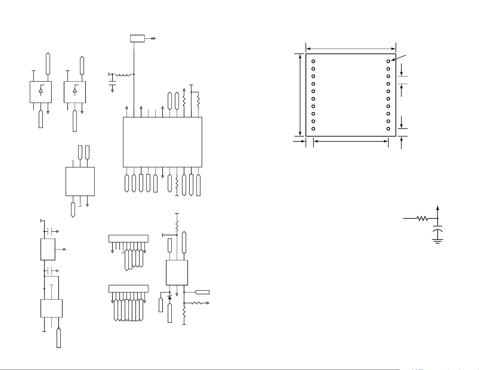
Figure 6: EVM-GPS-F4 PCB Layout Dimensions
(25.40)
Power Supply Requirements
The transceiver incorporates a precision
low-dropout regulator which allows operation
over a wide input voltage range. Despite this
regulator, it is still important to provide a supply
Vcc IN
that is free of noise. Power supply noise can
significantly affect the module’s performance, so
providing a clean power supply for the module
should be a high priority during design.
Figure 7: Supply Filter
A 10Ω resistor in series with the supply followed by a 10µF tantalum
capacitor from Vcc to ground helps in cases where the quality of supply
power is poor (Figure 7). This filter should be placed close to the module’s
supply lines. These values may need to be adjusted depending on the
noise present on the supply line.
Vcc TO
MODULE
10Ω
+
10µF
– –
4 5
– –
Page 6

(This page is intentionally blank.)(This page is intentionally blank.)
– –
6 7
– –
Page 7

Linx Technologies
159 Ort Lane
Merlin, OR, US 97532
Phone: +1 541 471 6256
Fax: +1 541 471 6251
www.linxtechnologies.com
Disclaimer
Linx Technologies is continually striving to improve the quality and function of its products. For this reason, we
reserve the right to make changes to our products without notice. The information contained in this Data Guide
is believed to be accurate as of the time of publication. Specifications are based on representative lot samples.
Values may vary from lot-to-lot and are not guaranteed. “Typical” parameters can and do vary over lots and
application. Linx Technologies makes no guarantee, warranty, or representation regarding the suitability of any
product for use in any specific application. It is the customer’s responsibility to verify the suitability of the part for
the intended application. NO LINX PRODUCT IS INTENDED FOR USE IN ANY APPLICATION WHERE THE SAFETY
OF LIFE OR PROPERTY IS AT RISK.
Linx Technologies DISCLAIMS ALL WARRANTIES OF MERCHANTABILITY AND FITNESS FOR A PARTICULAR
PURPOSE. IN NO EVENT SHALL LINX TECHNOLOGIES BE LIABLE FOR ANY OF CUSTOMER’S INCIDENTAL OR
CONSEQUENTIAL DAMAGES ARISING IN ANY WAY FROM ANY DEFECTIVE OR NON-CONFORMING PRODUCTS
OR FOR ANY OTHER BREACH OF CONTRACT BY LINX TECHNOLOGIES. The limitations on Linx Technologies’
liability are applicable to any and all claims or theories of recovery asserted by Customer, including, without
limitation, breach of contract, breach of warranty, strict liability, or negligence. Customer assumes all liability
(including, without limitation, liability for injury to person or property, economic loss, or business interruption) for
all claims, including claims from third parties, arising from the use of the Products. The Customer will indemnify,
defend, protect, and hold harmless Linx Technologies and its officers, employees, subsidiaries, affiliates,
distributors, and representatives from and against all claims, damages, actions, suits, proceedings, demands,
assessments, adjustments, costs, and expenses incurred by Linx Technologies as a result of or arising from any
Products sold by Linx Technologies to Customer. Under no conditions will Linx Technologies be responsible for
losses arising from the use or failure of the device in any application, other than the repair, replacement, or refund
limited to the original product purchase price. Devices described in this publication may contain proprietary,
patented, or copyrighted techniques, components, or materials. Under no circumstances shall any user be
conveyed any license or right to the use or ownership of such items.
©2015 Linx Technologies. All rights reserved.
The stylized Linx logo, Wireless Made Simple, WiSE, CipherLinx and the stylized CL logo are trademarks of Linx Technologies.
 Loading...