

Page 1

R4 Series
GPS Receiver Module
Data Guide
Page 2

Table of Contents
1 Description
1 Features
1 Applications
2 Ordering Information
2 Absolute Maximum Ratings
2 Electrical Specications
4 Pin Assignments
4 Pin Descriptions
5 A Brief Overview of GPS
5 Client Generated Extended Ephemeris (CGEE)
6 Time To First Fix (TTFF)
6 Module Description
7 Backup Battery
7 Power Supply Requirements
7 The 1PPS Output
8 Antenna Considerations
9 Power Control
10 Slow Start Time
10 Protocols
11 Interfacing with NMEA Messages
12 Interfacing with NMEA Messages
17 NMEA Input Messages
24 Typical Applications
25 Master Development System
26 Board Layout Guidelines
27 Pad Layout
28 Microstrip Details
29 Production Guidelines
29 Hand Assembly
Warning: Some customers may want Linx radio frequency (“RF”)
products to control machinery or devices remotely, including machinery
or devices that can cause death, bodily injuries, and/or property
damage if improperly or inadvertently triggered, particularly in industrial
settings or other applications implicating life-safety concerns (“Life and
Property Safety Situations”).
NO OEM LINX REMOTE CONTROL OR FUNCTION MODULE
SHOULD EVER BE USED IN LIFE AND PROPERTY SAFETY
SITUATIONS. No OEM Linx Remote Control or Function Module
should be modified for Life and Property Safety Situations. Such
modification cannot provide sufficient safety and will void the product’s
regulatory certification and warranty.
Customers may use our (non-Function) Modules, Antenna and
Connectors as part of other systems in Life Safety Situations, but
only with necessary and industry appropriate redundancies and
in compliance with applicable safety standards, including without
limitation, ANSI and NFPA standards. It is solely the responsibility
of any Linx customer who uses one or more of these products to
incorporate appropriate redundancies and safety standards for the Life
and Property Safety Situation application.
Do not use this or any Linx product to trigger an action directly
from the data line or RSSI lines without a protocol or encoder/
decoder to validate the data. Without validation, any signal from
another unrelated transmitter in the environment received by the module
could inadvertently trigger the action.
All RF products are susceptible to RF interference that can prevent
communication. RF products without frequency agility or hopping
implemented are more subject to interference. This module does not
have a frequency hopping protocol built in.
Do not use any Linx product over the limits in this data guide.
Excessive voltage or extended operation at the maximum voltage could
cause product failure. Exceeding the reflow temperature profile could
cause product failure which is not immediately evident.
Do not make any physical or electrical modifications to any Linx
product. This will void the warranty and regulatory and UL certifications
and may cause product failure which is not immediately evident.
!
Page 3
– –
1
Description
The R4 Series GPS receiver module is
a self-contained high-performance GPS
receiver. Based on the SiRFstar IV chipset,
it provides exceptional sensitivity, even
in dense foliage and urban canyons. The
module’s very low power consumption
helps maximize runtimes in battery
powered applications. With over 200,000
effective correlators, the R4 Series
receiver can acquire and track up to 48
satellites simultaneously in just seconds,
even at the lowest signal levels. Housed in a compact reflow-compatible
SMD package, the receiver requires no programming or additional RF
components (except an antenna) to form a complete GPS solution. The
module’s standard NMEA data output makes the R4 Series easy to
integrate, even by engineers without previous RF or GPS experience.
Features
• SiRF Star IV chipset
• Built-in jammer remover
• High sensitivity (–160dBm)
• 48 channels
• Fast TTFF at low signal levels
• Battery-backed SRAM
• CGEE allows 3-day prediction
• No programming necessary
• No external RF components
needed (except an antenna)
• No production tuning
• Direct serial interface
• Power down feature
• Compact surface-mount
package
• Manual or reflow compatible
Applications
• Positioning and Navigation
• Location and Tracking
• Security/Loss-Prevention
• Surveying
• Logistics
• Fleet Management
R4 Series GPS Receiver
Data Guide
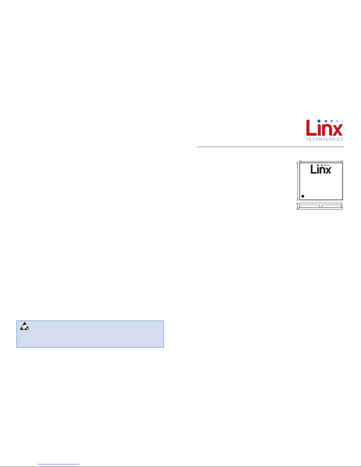
Figure 1: Package Dimensions
Revised 6/1/2016
GPS MODULE
RXM-GPS-R4
LOT GRxxxx
0.591
(15.00)
0.512
(13.00)
0.087
(2.20)
29 Automated Assembly
31 Resources
Warning: This product incorporates numerous static-sensitive
components. Always wear an ESD wrist strap and observe proper ESD
handling procedures when working with this device. Failure to observe
this precaution may result in module damage or failure.
Page 4
– –
– –
2 3
Ordering Information
Ordering Information
Part Number Description
RXM-GPS-R4-x R4 Series GPS Receiver Module
MDEV-GPS-R4 R4 Series GPS Receiver Master Development System
EVM-GPS-R4 R4 Series GPS Receiver Evaluation Module
x = “T” for Tape and Reel, “B” for Bulk
Reels are 1,000 pieces
Quantities less than 1,000 pieces are supplied in bulk
Figure 2: Ordering Information
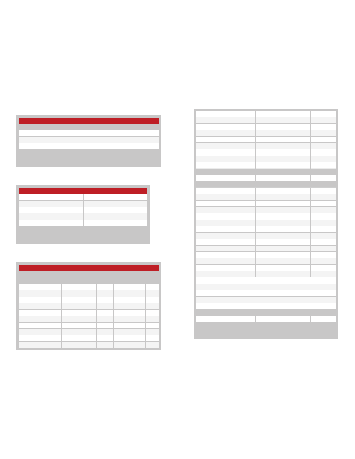
Figure 4: Figure 3: Electrical Specifications
Absolute Maximum Ratings
Supply Voltage V
CC
+4.3 VDC
Input Battery Backup Voltage +7.0 VDC
Operating Temperature −40 to +85 ºC
Storage Temperature −40 to +85 ºC
Soldering Temperature +225°C for 10 seconds
Exceeding any of the limits of this section may lead to permanent damage to the
device. Furthermore, extended operation at these maximum ratings may reduce
the life of this device.
Absolute Maximum Ratings
Figure 3: Absolute Maximum Ratings
R4 Series GPS Receiver Specifications
Parameter Symbol Min. Typ. Max. Units Notes
Power Supply
Operating Voltage V
CC
3.0 3.3 3.6 VDC
Supply Current l
CC
Peak 122 mA 1
Acquisition 56 mA 1
Tracking 33 mA 1
Hibernate 0.43 mA 1
Backup Battery Voltage V
BAT
2.0 6.0 VDC
Backup Battery Current I
BAT
660 830 µA 2
VOUT Output Voltage V
OUT
VCC 3
Output Low Voltage V
OL
0.4 VDC
Electrical Specications
Output High Voltage V
OH
TX Pin 0.7*VCC VCC VCC VDC
1.8V Level Pin 1.2 1.8 1.85 VDC
Output Low Current I
OL
2.0 mA
Output High Current I
OH
TX Pin 0.05 mA
1.8V Level Pin 2.0 mA
Input Low Voltage V
IL
–0.4 0.45 VDC
Input High Voltage V
IH
1.3 3.6 VDC
LNA Section
Input Power P
IN
18 dB
Receiver Section
Receiver Sensitivity
Tracking –160 dBm
Navigation –157 dBm
Cold Start –145 dBm
Acquisition Time
Hot Start (Open Sky) 1 s
Hot Start (Indoor) 15 s
Cold Start 32 s
Cold Start, CGEE 15 s
Position Accuracy
Autonomous 2.5 m
SBAS 2.5 m
Altitude 18,000 m
Velocity 515 m/s
Chipset SiRF Star IV, GSD4e ROM
Frequency L1 1575.42MHz, C/A Code
Channels 48
Update Rate 1Hz default, up to 5Hz
Protocol Support NMEA 0183 ver 3.0, SiRF Binary
Antenna Port
RF Impedance R
IN
50 Ω
1. VCC = 3.3V, without active antenna
2. VCC = 0V
3. VOUT current is directly sourced from VCC.
Page 5
– –
– –
4 5
NC1
NC2
1PPS3
TX4
RX5
GND21
NC6
1PPS7
/RESET8
RFPWRUP9
ON_OFF10
GND 20
RFIN 19
GND 18
VOUT 17
NC 16
GND 22
NC 15
NC 14
NC 13
VCC 12
VBACKUP 11
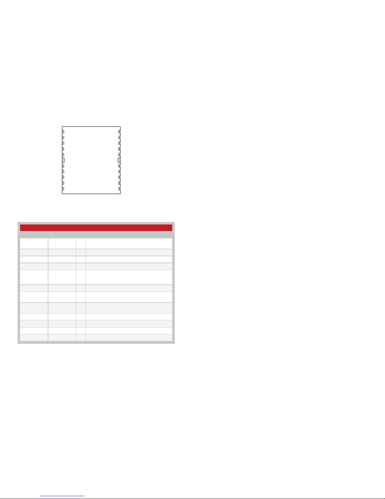
Figure 5: R4 Series GPS Receiver Pinout (Top View)
Figure 6: R4 Series GPS Receiver Pin Descriptions
Pin Assignments
Pin Descriptions
Pin Descriptions
Pin Number Name I/O Description
1, 2, 6, 13,
14, 15, 16
NC − No electrical connection.
3, 7 1PPS O 1 Pulse Per Second. 1.8V level.
4 TX O Serial output (default NMEA)
5 RX I Serial input (default NMEA)
8 /RESET I
Reset input, active low. The module has an
internal power-on reset circuit so this pin can be
left floating
9 RFPWRUP O Power State Indicator. 1.8V level.
10 ON_OFF I
Power Control Pin. If this pin is not used, leave it
floating.
11 VBACKUP P
Backup battery supply voltage. This line must be
powered to enable the module.
12 VCC P Supply Voltage
18, 20, 21, 22 GND P Ground
17 VOUT O VCC voltage to supply an active antenna.
19 RFIN I GPS RF signal input
A Brief Overview of GPS
The Global Positioning System (GPS) is a U.S.-owned utility that freely and
continuously provides positioning, navigation, and timing (PNT) information.
Originally created by the U.S. Department of Defense for military
applications, the system was made available without charge to civilians
in the early 1980s. The global positioning system consists of a nominal
constellation of 24 satellites orbiting the earth at about 12,000 nautical
miles in height. The pattern and spacing of the satellites allow at least four
to be visible above the horizon from any point on the Earth. Each satellite
transmits low power radio signals which contain three different bits of
information; a pseudorandom code identifying the satellite, ephemeris data
which contains the current date and time as well as the satellite’s health,
and the almanac data which tells where each satellite should be at any time
throughout the day.
A GPS receiver receives and times the signals sent by multiple satellites
and calculates the distance to each satellite. If the position of each satellite
is known, the receiver can use triangulation to determine its position
anywhere on the earth. The receiver uses four satellites to solve for four
unknowns; latitude, longitude, altitude and time. If any of these factors is
already known to the system, an accurate position (fix) can be obtained
with fewer satellites in view. Tracking more satellites improves calculation
accuracy. In essence, the GPS system provides a unique address for every
square meter on the planet.
A faster Time To First Fix (TTFF) is also possible if the satellite information
is already stored in the receiver. If the receiver knows some of this
information, then it can accurately predict its position before acquiring an
updated position fix. For example, aircraft or marine navigation equipment
may have other means of determining altitude, so the GPS receiver would
only have to lock on to three satellites and calculate three equations to
provide the first position fix after power-up.
Client Generated Extended Ephemeris (CGEE)
CGEE is a type of assisted GPS (AGPS) where the receiver uses the
ephemeris data broadcast by the satellites to calculate models of each
visible satellite’s future location. This allows the receiver to store up to 3
days worth of ephemeris data and results in faster TTFF.
Page 6

– –
– –
6 7
Time To First Fix (TTFF)
TTFF is often broken down into three parts:
Cold: A cold start is when the receiver has no accurate knowledge of its
position or time. This happens when the receiver’s internal Real Time Clock
(RTC) has not been running or it has no valid ephemeris or almanac data.
In a cold start, the receiver takes 35 to 40 seconds to acquire its position.
Warm or Normal: A typical warm start is when the receiver has valid
almanac and time data and has not significantly moved since its last valid
position calculation. This happens when the receiver has been shut down
for more than 2 hours, but still has its last position, time, and almanac
saved in memory, and its RTC has been running. The receiver can predict
the location of the current visible satellites and its location; however, it
needs to wait for an ephemeris broadcast (every 30 seconds) before it can
accurately calculate its position.
Hot or Standby: A hot start is when the receiver has valid ephemeris, time,
and almanac data. This happens when the receiver has been shut down
for less than 2 hours and has the necessary data stored in memory with
the RTC running. In a hot start, the receiver takes 1 second to acquire its
position. The time to calculate a fix in this state is sometimes referred to as
Time to Subsequent Fix or TTSF.
Module Description
The R4 Series GPS Receiver module is based on the SiRFstarIV chipset,
which consumes less power than competitive products while providing
exceptional performance even in dense foliage and urban canyons. No
external RF components are needed other than an antenna. The simple
serial interface and industry standard NMEA protocol make integration of
the R4 Series receiver into an end product extremely straightforward.
The module’s high-performance RF architecture allows it to receive GPS
signals that are as low as –160dBm. The R4 Series can track up to 48
satellites at the same time. Once locked onto the visible satellites, the
receiver calculates the range to the satellites and determines its position
and the precise time. It then outputs the data through a standard serial port
using several standard NMEA protocol formats.
The GPS core handles all of the necessary initialization, tracking, and
calculations autonomously, so no programming is required. The RF section
is optimized for low level signals, and requires no production tuning.
Backup Battery
The module is designed to work with a backup battery that keeps the
SRAM memory and the RTC powered when the RF section and the main
GPS core are powered down. This enables the module to have a faster
Time To First Fix (TTFF) when it is powered back on. The memory and
clock pull about 660µA. This means that a small lithium battery is sufficient
to power these sections. This significantly reduces the power consumption
and extends the main battery life while allowing for fast position fixes when
the module is powered back on.
The backup battery must be installed for CGEE start. If the serial command
is used to place the receiver into hibernate while keeping VCC powered,
then the battery backup current is 15µA while the current through the VCC
line is about 170µA.
Power Supply Requirements
The module requires a clean, well-regulated power source. While it is
preferable to power the unit from a battery, it can operate from a power
supply as long as noise is less than 20mV. Power supply noise can
significantly affect the receiver’s sensitivity, therefore providing clean power
to the module should be a high priority during design. Bypass capacitors
should be placed as close as possible to the module. The values should be
adjusted depending on the amount and type of noise present on the supply
line.
The 1PPS Output
The 1PPS line outputs 1 pulse per second on the rising edge of the GPS
second when the receiver has an over-solved navigation solution from
five or more satellites. The pulse has a duration of 200ms with the rising
edge on the GPS second. This line is low until the receiver acquires an
over-solved navigation solution (a lock on more than 4 satellites). The
GPS second is based on the atomic clocks in the GPS satellites, which
are monitored and set to Universal Time master clocks. This output and
the time calculated from the GPS satellite transmissions can be used as a
clock feature in an end product.
Page 7

– –
– –
8 9
Antenna Considerations
The R4 Series module is designed to utilize a wide variety of external
antennas. The module has a regulated power output which simplifies
the use of GPS antenna styles which require external power. This allows
the designer great flexibility, but care must be taken in antenna selection
to ensure optimum performance. For example, a handheld device may
be used in many varying orientations so an antenna element with a wide
and uniform pattern may yield better overall performance than an antenna
element with high gain and a correspondingly narrower beam. Conversely,
an antenna mounted in a fixed and predictable manner may benefit from
pattern and gain characteristics suited to that application. Evaluating
multiple antenna solutions in real-world situations is a good way to rapidly
assess which will best meet the needs of your application.
For GPS, the antenna should have good right hand circular polarization
characteristics (RHCP) to match the polarization of the GPS signals.
Ceramic patches are the most commonly used style of antenna, but
there are many different shapes, sizes and styles of antennas available.
Regardless of the construction, they will generally be either passive or
active types. Passive antennas are simply an antenna tuned to the correct
frequency. Active antennas add a Low Noise Amplifier (LNA) after the
antenna and before the module to amplify the weak GPS satellite signals.
For active antennas, a 300 ohm ferrite bead can be used to connect the
VOUT line to the RFIN line. This bead prevents the RF from getting into the
power supply, but allows the DC voltage onto the RF trace to feed into the
antenna. A series capacitor inside the module prevents this DC voltage
from affecting the bias on the module’s internal LNA. The VOUT line is
connected to the VCC line, so the voltage is the module supply voltage and
the current sourcing depends on the module’s power supply.
Maintaining a 50 ohm path between the module and antenna is critical.
Errors in layout can significantly impact the module’s performance. Please
review the layout guidelines elsewhere in this guide carefully to become
more familiar with these considerations.
Power Control
The R4 Series GPS Receiver module offers two power control modes: Full
Power and Hibernate. In Full Power mode the module is fully active and
and continuously tracking. Measurements are of the highest quality and are
continuously output by the module. This is the highest current consumption
state.
Hibernate mode is the lowest power setting. The tracking and processor
blocks are powered down, but the RTC is still running and the memory
blocks are still powered enabling a hot start.
The module switches between these states by toggling the ON_OFF line.
The ON_OFF line must go high for at least 100ms to trigger the change of
state and must remain low for at least 100ms to reset the edge detector.
If the module is in Full Power mode, a pulse on the ON_OFF line will initiate
an orderly shutdown into Hibernate mode. If the module is in Hibernate
mode, a pulse on the ON_OFF line will transistion the module into Full
Power Mode.
ON_OFF
Full PowerHibernate Full Power
Module
Power
100ms 100ms
Figure 7: R4 Series GPS Receiver Power Control
Page 8

– –
– –
10 11
Slow Start Time
The most critical factors in start time are current ephemeris data, signal
strength and sky view. The ephemeris data describes the path of each
satellite as they orbit the earth. This is used to calculate the position of
a satellite at a particular time. This data is only usable for a short period
of time, so if it has been more than a few hours since the last fix or if the
location has significantly changed (a few hundred miles), then the receiver
may need to wait for a new ephemeris transmission before a position can
be calculated. The GPS satellites transmit the ephemeris data every 30
seconds. Transmissions with a low signal strength may not be received
correctly or be corrupted by ambient noise. The view of the sky is important
because the more satellites the receiver can see, the faster the fix and the
more accurate the position will be when the fix is obtained.
If the receiver is in a very poor location, such as inside a building, urban
canyon, or dense foliage, then the time to first fix can be slowed. In very
poor locations with poor signal strength and a limited view of the sky with
outdated ephemeris data, this could be on the order of several minutes.
In the worst cases, the receiver may need to receive almanac data, which
describes the health and course data for every satellite in the constellation.
This data is transmitted every 15 minutes. If a lock is taking a long time, try
to find a location with a better view of the sky and fewer obstructions. Once
locked, it is easier for the receiver to maintain the position fix.
Protocols
Linx GPS modules use the SiRFstar IV chipset. This chipset allows two
protocols to be used, NMEA-0183 and SiRF Binary. Switching between the
two is handled using a single serial command. The NMEA protocol uses
ASCII characters for the input and output messages and provides the most
common features of GPS development in a small command set. The SiRF
Binary protocol uses BYTE data types and allows more detailed control
over the GPS receiver and its functionality using a much larger command
set. Although both protocols have selectable baud rates, it’s recommended
that SiRF Binary use 115,200bps. For a detailed description of the SiRF
Binary protocol, see the SiRF Binary Protocol Reference Manual, available
from SiRF Technology, Inc.
Note: Although SiRF Binary protocol may be used with the module,
Linx only offers tech support for the NMEA protocol.
Interfacing with NMEA Messages
Linx modules default to the NMEA protocol. Output messages are sent
from the receiver on the TX pin and input messages are sent to the receiver
on the RX pin. By default, output messages are sent once every second.
Details of each message are described in the following sections.
The NMEA message format is as follows: <Message-ID + Data Payload +
Checksum + End Sequence>. The serial data structure defaults to
9,600bps, 8 data bits, 1 start bit, 2 stop bits, and no parity. Each message
starts with a $ character and ends with a <CR> <LF>. All fields within
each message are separated by a comma. The checksum follows the *
character and is the last two characters, not including the <CR> <LF>.
It consists of two hex digits representing the exclusive OR (XOR) of all
characters between, but not including, the $ and * characters. When
reading NMEA output messages, if a field has no value assigned to it, the
comma will still be placed following the previous comma. For example,
{,04,,,,,2.0,} shows four empty fields between values 04 and 2.0. When
writing NMEA input messages, all fields are required, none are optional. An
empty field will invalidate the message and it will be ignored.
Reading NMEA output messages:
• Initialize a serial interface to match the serial data structure of the GPS
receiver.
• Read the NMEA data from the TX pin into a receive buffer.
• Separate it into six buffers, one for each message type. Use the
characters ($) and <CR> <LF> as end points for each message.
• For each message, calculate the checksum as mentioned above to
compare with the received checksum.
• Parse the data from each message using commas as field separators.
• Update the application with the parsed field values.
• Clear the receive buffer and be ready for the next set of messages.
Writing NMEA input messages:
• Initialize a serial interface to match the serial data structure of the GPS
receiver.
• Assemble the message to be sent with the calculated checksum.
• Transmit the message to the receiver on the RX pin.
Page 9

– –
– –
12 13
NMEA Output Messages
The following sections outline the data structures of the various NMEA
messages that are supported by the module. By default, the commands
are at 9,600bps, 8 data bits, 1 start bit, 2 stop bits, and no parity.
GGA – Global Positioning System Fixed Data
Figure 8 contains the values for the following example:
$GPGGA,053740.000,2503.6319,N,12136.0099,E,1,08,1.1,63.8,M,15.2,M,,0000*64
Global Positioning System Fixed Data Example
Name Example Units Description
Message ID $GPGGA GGA protocol header
UTC Time 053740.000 hhmmss.sss
Latitude 2503.6319 ddmm.mmmm
N/S Indicator N N=north or S=south
Longitude 12136.0099 dddmm.mmmm
E/W Indicator E E=east or W=west
Position Fix Indicator 1 See Figure 9
Satellites Used 08 Range 0 to 12.
HDOP 1.1 Horizontal Dilution of Precision
MSL Altitude 63.8 meters
Units M meters
Geoid Separation 15.2 meters
Units M meters
Age of Diff. Corr. second Null fields when DGPS is not used
Diff. Ref. Station 0000
Checksum *64
<CR> <LF> End of message termination
Figure 8: Global Positioning System Fixed Data Example
Position Indicator Values
Value Description
0 Fix not available or invalid
1 GPS SPS Mode, fix valid
2 Differential GPS, SPS Mode, fix valid
3–5 Not supported
6 Dead Reckoning Mode, fix valid
Figure 9: Position Indicator Values
GLL – Geographic Position – Latitude / Longitude
Figure 10 contains the values for the following example:
$GPGLL,2503.6319,N,12136.0099,E,053740.000,A,A*52
GSA – GPS DOP and Active Satellites
Figure 11 contains the values for the following example:
$GPGSA,A,3,24,07,17,11,28,08,20,04,,,,,2.0,1.1,1.7*35
GPS DOP and Active Satellites Example
Name Example Units Description
Message ID $GPGSA GSA protocol header
Mode 1 A See Figure 12
Mode 2 3 1=No fix, 2=2D, 3=3D
ID of satellite used 24 Sv on Channel 1
ID of satellite used 07 Sv on Channel 2
... ...
ID of satellite used Sv on Channel 12
PDOP 2.0 Position Dilution of Precision
HDOP 1.1 Horizontal Dilution of Precision
VDOP 1.7 Vertical Dilution of Precision
Checksum *35
<CR> <LF> End of message termination
Figure 10: Geographic Position – Latitude / Longitude Example
Geographic Position – Latitude / Longitude Example
Name Example Units Description
Message ID $GPGLL GLL protocol header
Latitude 2503.6319 ddmm.mmmm
N/S Indicator N N=north or S=south
Longitude 12136.0099 dddmm.mmmm
E/W Indicator E E=east or W=west
UTC Time 053740.000 hhmmss.sss
Status A A=data valid or V=data not valid
Mode A
A=autonomous, D=DGPS, N=Data
not valid
Checksum *52
<CR> <LF> End of message termination
Figure 11: GPS DOP and Active Satellites Example
Page 10

– –
– –
14 15
GSV – GPS Satellites in View
Figure 13 contains the values for the following example:
$GPGSV,3,1,12,28,81,285,42,24,67,302,46,31,54,354,,20,51,077,46*73
$GPGSV,3,2,12,17,41,328,45,07,32,315,45,04,31,250,40,11,25,046,41*75
$GPGSV,3,3,12,08,22,214,38,27,08,190,16,19,05,092,33,23,04,127,*7B
Mode 1 Values
Value Description
M Manual – forced to operate in 2D or 3D mode
A Automatic – allowed to automatically switch 2D/3D
Figure 13: GPS Satellites in View Example
GPS Satellites in View Example
Name Example Units Description
Message ID $GPGSV GSV protocol header
Total number of
messages
1
3 Range 1 to 3
Message number
1
1 Range 1 to 3
Satellites in view 12
Satellite ID 28 Channel 1 (Range 01 to 196)
Elevation 81 degrees Channel 1 (Range 00 to 90)
Azimuth 285 degrees Channel 1 (Range 000 to 359)
SNR (C/No) 42 dB-Hz
Channel 1 (Range 00 to 99, null when
not tracking)
Satellite ID 20 Channel 4 (Range 01 to 32)
Elevation 51 degrees Channel 4 (Range 00 to 90)
Azimuth 077 degrees Channel 4 (Range 00 to 359)
SNR (C/No) 46 dB-Hz
Channel 4 (Range 00 to 99, null when
not tracking.
Checksum *73
<CR> <LF> End of message termination
1. Depending on the number of satellites tracked, multiple messages of GSV data
may be required.
Figure 12: Mode 1 Values
RMC – Recommended Minimum Specific GPS Data
Figure 14 contains the values for the following example:
$GPRMC,053740.000,A,2503.6319,N,12136.0099,E,2.69,79.65,100106,,,A*53
Recommended Minimum Specific GPS Data Example
Name Example Units Description
Message ID $GPRMC RMC protocol header
UTC Time 053740.000 hhmmss.sss
Status A A=data valid or V=data not valid
Latitude 2503.6319 ddmm.mmmm
N/S Indicator N N=north or S=south
Longitude 12136.0099 dddmm.mmmm
E/W Indicator E E=east or W=west
Speed over ground 2.69 knots TRUE
Course over ground 79.65 degrees
Date 100106 ddmmyy
Magnetic Variation degrees Not available, null field
Variation Sense E=east or W=west (not shown)
Mode A
A=autonomous, D=DGPS, N= Data
not valid
Checksum *53
<CR> <LF> End of message termination
Figure 14: Recommended Minimum Specific GPS Data Example
Page 11

– –
– –
16 17
VTG – Course Over Ground and Ground Speed
Figure 15 contains the values for the following example:
$GPVTG,79.65,T,,M,2.69,N,5.0,K,A*38
Course Over Ground and Ground Speed Example
Name Example Units Description
Message ID $GPVTG VTG protocol header
Course over ground 79.65 degrees Measured heading
Reference T TRUE
Course over ground degrees Measured heading (N/A, null field)
Reference M Magnetic
Speed over ground 2.69 knots Measured speed
Units N Knots
Speed over ground 5.0 km/hr Measured speed
Units K Kilometer per hour
Mode A
A=autonomous, D=DGPS, N= Data
not valid
Checksum *38
<CR> <LF> End of message termination
Figure 15: Course Over Ground and Ground Speed Example
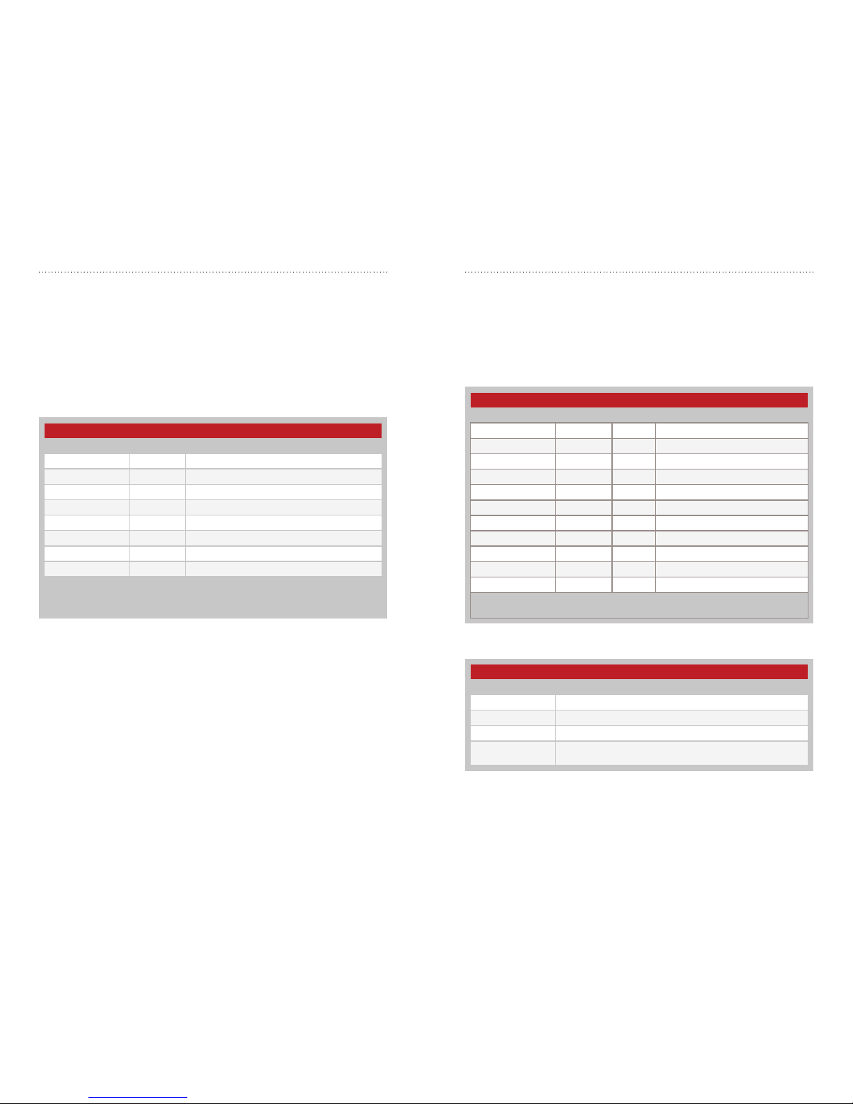
NMEA Input Messages
The following outlines the serial commands input into the module for
configuration. By default, the commands are input at 9,600bps, 8 data bits,
1 start bit, 2 stop bits, and no parity.
All fields in all proprietary NMEA messages are required; none are optional.
All NMEA messages are comma delimited. Figure 17 outlines the message
identifiers supported by the module.
Serial Data Structure
Name Example Description
Start Sequence $PSRF
Message ID <MID>
Message Identifier consisting of three numeric
characters. Input messages begin at MID 100.
Payload DATA Message specific data.
Checksum CKSUM
CKSUM is a two-hex character checksum as
defined in the NMEA specification, NMEA-0183
Standard for Interfacing Marine Electronic Devices.
Checksums are required on all input messages.
End Sequence <CR> <LF>
Each message must be terminated using Carriage
Return (CR) Line Feed (LF) (\r\n, 0x0D0A) to cause
the receiver to process the input message. They
are not printable ASCII characters, so are omitted
from the examples.
Figure 16: Serial Data Structure
Message ID Values
Name MID Description
SetSerialPort 100 Set PORT A parameters and protocol
NavigationInitialization 101 Reset the modules
Query/Rate Control 103
Query standard NMEA message and/or set
output rate
LLANavigationInitialization 104 Reset the modules
Development Data On/Off 105 Development Data messages On/Off
System Turn Off 117
Performs an orderly shut down of the module
and switches into hibernation mode
Figure 17: Message ID Values
Page 12
– –
– –
18 19
100 – SetSerialPort
This command message is used to set the protocol (SiRF binary or NMEA)
and/or the communication parameters (baud rate). Generally, this
command is used to switch the module back to SiRF binary protocol mode
where a more extensive command message set is available. When a valid
message is received, the parameters are stored in battery-backed SRAM
and the receiver restarts using the saved parameters.
Figure 18 contains the values for the following example:
Switch to SiRF binary protocol at 9600,8,N,1
$PSRF100,0,9600,8,1,0*0C
For details on the SiRF binary protocol, please refer to SiRF’s Binary
Protocol Reference Manual.
SetSerialPort Example
Name Example Description
Message ID $PSRF100 PSRF100 protocol header
Protocol 0 0=SiRF binary, 1=NMEA
Baud 9600 4800, 9600, 19200, 38400, 57600, 115200
DataBits 8 8
1
StopBits 1 0, 1
1
Parity 0 0=None, 1=Odd, 2=Even
1
Checksum *0C
<CR> <LF> End of message termination
1. SiRF protocol is only valid for 8 data bits, 1 stop bit and no parity.
2. Default settings are NMEA protocol using 9,600 baud, 8 data bits, 2 stop bits and no
parity.
Figure 18: SetSerialPort Example
101 – NavigationInitialization
This command is used to initialize the receiver with the current position (in
X, Y, Z coordinates), clock offset, and time, enabling a faster fix. Increased
receiver sensitivity and the removal of Selective Availability (SA) have made
this unneccessary. The command is retained for its ability to reset the
module, but the initialization fields are no longer supported.
Figure 19 contains the values for the following example:
$PSRF101,-2686700,-4304200,3851624,96000,497260,921,12,3*1C
Figure 19: NavigationInitialization Example
NavigationInitialization Example
Name Example Units Description
Message ID $PSRF101 PSRF101 protocol header
ECEF X -2686700 meters X coordinate position
ECEF Y -4304200 meters Y coordinate position
ECEF Z 3851624 meters Z coordinate position
ClkOffset 96000 Hz Clock Offset
1
TimeOfWeek 497260 seconds GPS Time Of Week
WeekNo 921 GPS Week Number
ChannelCount 12 Range 1 to 12
ResetCfg 3 See Figure 20
Checksum *1F
<CR> <LF> End of message termination
1. Use 0 for the last saved value if available. If this is unavailable, a default value of
96000 is used.
ResetCfg Values
Hex Description
0x01 Hot Start – All data valid
0x02 Warm Start – Ephemeris cleared
0x04 Cold Start – Clears all data in memory
0x08
Clear Memory – Clears all data in memory and resets the receiver
back to factory defaults
Figure 20: ResetCfg Values
Page 13

– –
– –
20 21
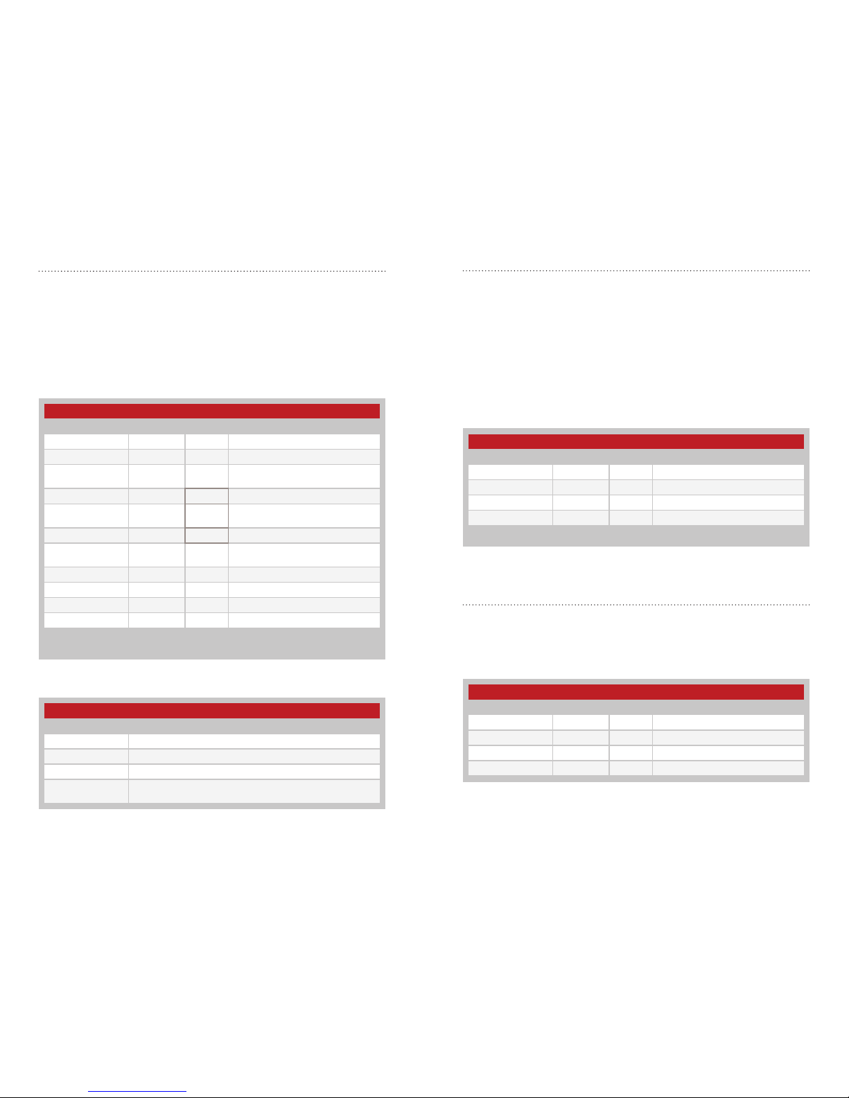
Update Rate Control Example
1
Name Example Units Description
Message ID $PSRF103 PSRF103 protocol header
Msg 00 See Figure 22
Mode 01
0=SetRate, 1=Query, 6=Enable
divider2, 7=Disable divider
Rate
3
00 seconds Output: off=0, max=255
CksumEnable 01 0=Disable, 1=Enable Checksum
Checksum *25
<CR> <LF> End of message termination
1. Default setting is GGA, GLL, GSA, GSV, RMC and VTG NMEA messages are enabled
with checksum at a rate of 1 second.
2. Enabling the rate divider divides the rate value by 5.
3. Rate value sets the period of a single transmission. For maximum update rate (5Hz)
enter a value of 1 and enable the rate divider.
103 – Update Rate Control
This command is used to control the output of standard NMEA messages
GGA, GLL, GSA, GSV, RMC and VTG. Using this command message,
standard NMEA messages may be polled once, or setup for periodic
output. Checksums may also be enabled or disabled depending on the
needs of the receiving program. NMEA message settings are saved in
battery-backed memory for each entry when the message is accepted.
Figure 21 contains the values for the following example:
1. Query the GGA message with checksum enabled
$PSRF103,00,01,00,01*25
2. Enable VTG message for a 1Hz constant output with checksum
enabled
$PSRF103,05,00,01,01*20
3. Disable VTG message
$PSRF103,05,00,00,01*21
4. Enable 5Hz mode
$PSRF103,0,6,0,0*23
5. Disable 5Hz mode
$PSRF103,0,7,0,0*22
Figure 21: Update Rate Control Example
Note: When using 5Hz mode, it is recommended to disable any
unused NMEA message types (see example 3) and set the serial port
to maximum baud rate (see Figure 18). The rate divider takes effect
only after a fix is established
MSGValues
Value Description
0 GGA
1 GLL
2 GSA
3 GSV
4 RMC
5 VTG
6 MSS (not supported)
7 Not defined
8 ZDA
9 Not defined
Figure 22: MSG Values
Page 14
– –
– –
22 23
104 – LLANavigationInitialization
This command is used to initialize the receiver with the current position
(in lattitude, longitude and altitude coordinates), clock offset, and time,
enabling a faster fix. Increased receiver sensitivity and the removal of
Selective Availability (SA) have made this unneccessary. The command is
retained for its ability to reset the module, but the initialization fields are no
longer supported.
Figure 23 contains the values for the following example:
$PSRF104,37.3875111,-121.97232,0,96000,237759,1946,12,1*07
Figure 23: NavigationInitialization Example
LLANavigationInitialization Example
Name Example Units Description
Message ID $PSRF104 PSRF104 protocol header
Latitude 37.3875111 degrees Latitude position (Range 90 to –90)
Longitude
–121.97232 degrees
Longitude position (Range 180 to
–180)
Altitude 0 meters Altitude position
ClkOffset 96000 Hz
Clock Offset of the Evaluation
Receiver1
TimeOfWeek 237759 seconds GPS Time Of Week
WeekNo 1946
Extended GPS Week Number (1024
added)
ChannelCount 12 Range 1 to 12
ResetCfg 1 See Figure 24
Checksum *07
<CR> <LF> End of message termination
1. Use 0 for the last saved value if available. If this is unavailable, a default value of
96000 is used.
Figure 24: ResetCfg Values
ResetCfg Values
Hex Description
0x01 Hot Start – All data valid
0x02 Warm Start – Ephemeris cleared
0x04 Cold Start – Clears all data in memory
0x08
Clear Memory – Clears all data in memory and resets the receiver
back to factory defaults
105 – Development Data On / Off
Use this command to enable development data information if you are
having trouble getting commands accepted. Invalid commands generate
debug information that helps to determine the source of the command
rejection. Common reasons for input command rejection are invalid
checksum or parameter out of specified range.
Figure 25 contains the values for the following example:
1. Debug On
$PSRF105,1*3E
2. Debug Off
$PSRF105,0*3F
117 – System Turn Off
This message requests that the GPS receiver perform an orderly shutdown
and switch to hibernate mode.
Figure 26 contains the values for the following example:
$PSRF117,16*0B
Figure 25: Development Data On / Off Example
Development Data On / Off Example
1
Name Example Units Description
Message ID $PSRF105 PSRF105 protocol header
Debug 1 0=Off, 1=On
Checksum *3E
<CR> <LF> End of message termination
1. Default setting is debug mode off.
System Turn Off Example
Name Example Units Description
Message ID $PSRF117 PSRF117 protocol header
Sub ID 16 16: System turn off
Checksum *0B
<CR> <LF> End of message termination
Figure 26: System Turn Off Example
Page 15
– –
– –
24 25
Typical Applications
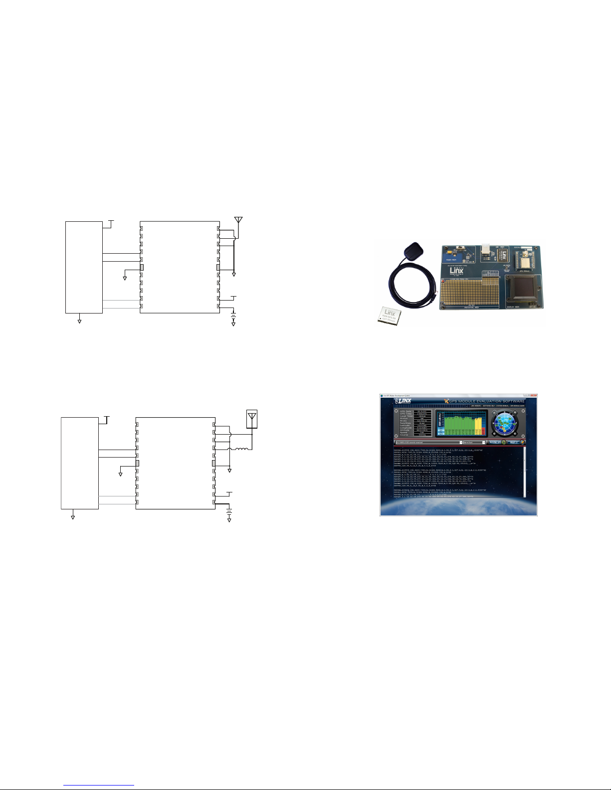
Figure 27 shows the R4 Series GPS receiver in a typical application using a
passive antenna.
A microcontroller UART is connected to the receiver’s UART for passing
data and commands. A 3.3V coin cell battery is connected to the
VBACKUP line to provide power to the module’s memory when main
power is turned off.
Figure 28 shows the module using an active antenna.
A 300Ω ferrite bead is used to put power from VOUT onto the antenna line
to power the active antenna.
Master Development System
The R4 Series Master Development System provides all of the tools
necessary to evaluate the R4 Series GPS receiver module. The system
includes a fully assembled development board, an active antenna,
development software and full documentation.
The development board includes a power supply, a prototyping area for
custom circuit development, and an OLED display that shows the GPS
data without the need for a computer. A USB interface is also included
for use with a PC running custom software or the included development
software.
The Master Development System software enables configuration of the
receiver and displays the satellite data output by the receiver. The software
can select from among all of the supported NMEA protocols for display of
the data.
Full documentation for the board and software is included in the
development system, making integration of the module straightforward.
Figure 29: The R4 Series Master Development System
Figure 30: The R4 Series Master Development System Software
NC
1
NC
2
1PPS
3
TX
4
RX
5
GND
21
NC
6
1PPS
7
/RESET
8
RFPWRUP
9
ON_OFF
10
GND
20
RFIN
19
GND
18
VOUT
17
NC
16
GND
22
NC
15
NC
14
NC
13
VCC
12
VBACKUP
11
µP
TX
RX
GND
VCC
GND
GND
VCC
GND
VCC
GND
300Ω
Ferrite Bead
Optional
OUT
IN
NC
1
NC
2
1PPS
3
TX
4
RX
5
GND
21
NC
6
1PPS
7
/RESET
8
RFPWRUP
9
ON_OFF
10
GND
20
RFIN
19
GND
18
VOUT
17
NC
16
GND
22
NC
15
NC
14
NC
13
VCC
12
VBACKUP
11
µP
TX
RX
GND
VCC
GND
GND
VCC
GND
VCC
GND
Optional
OUT
IN
Figure 27: Circuit Using the R4 Series Module with a Passive Antenna
Figure 28: Circuit Using the R4 Series Module with a an Active Antenna
Page 16
– –
– –
26 27
Board Layout Guidelines
The module’s design makes integration straightforward; however, it
is still critical to exercise care in PCB layout. Failure to observe good
layout techniques can result in a significant degradation of the module’s
performance. A primary layout goal is to maintain a characteristic
50-ohm impedance throughout the path from the antenna to the module.
Grounding, filtering, decoupling, routing and PCB stack-up are also
important considerations for any RF design. The following section provides
some basic design guidelines which may be helpful.
During prototyping, the module should be soldered to a properly laid-out
circuit board. The use of prototyping or “perf” boards will result in poor
performance and is strongly discouraged.
The module should, as much as reasonably possible, be isolated from
other components on your PCB, especially high-frequency circuitry such as
crystal oscillators, switching power supplies, and high-speed bus lines.
When possible, separate RF and digital circuits into different PCB regions.
Make sure internal wiring is routed away from the module and antenna, and
is secured to prevent displacement.
Do not route PCB traces directly under the module. There should not be
any copper or traces under the module on the same layer as the module,
just bare PCB. The underside of the module has traces and vias that could
short or couple to traces on the product’s circuit board.
The Pad Layout section shows a typical PCB footprint for the module. A
ground plane (as large and uninterrupted as possible) should be placed on
a lower layer of your PC board opposite the module. This plane is essential
for creating a low impedance return for ground and consistent stripline
performance.
Use care in routing the RF trace between the module and the antenna or
connector. Keep the trace as short as possible. Do not pass under the
module or any other component. Do not route the antenna trace on
multiple PCB layers as vias will add inductance. Vias are acceptable for
tying together ground layers and component grounds and should be used
in multiples.
Each of the module’s ground pins should have short traces tying
immediately to the ground plane through a via.
Bypass caps should be low ESR ceramic types and located directly
adjacent to the pin they are serving.
A 50-ohm coax should be used for connection to an external antenna.
A 50-ohm transmission line, such as a microstrip, stripline or coplanar
waveguide should be used for routing RF on the PCB. The Microstrip
Details section provides additional information.
In some instances, a designer may wish to encapsulate or “pot” the
product. There is a wide variety of potting compounds with varying
dielectric properties. Since such compounds can considerably impact
RF performance and the ability to rework or service the product, it is
the responsibility of the designer to evaluate and qualify the impact and
suitability of such materials.
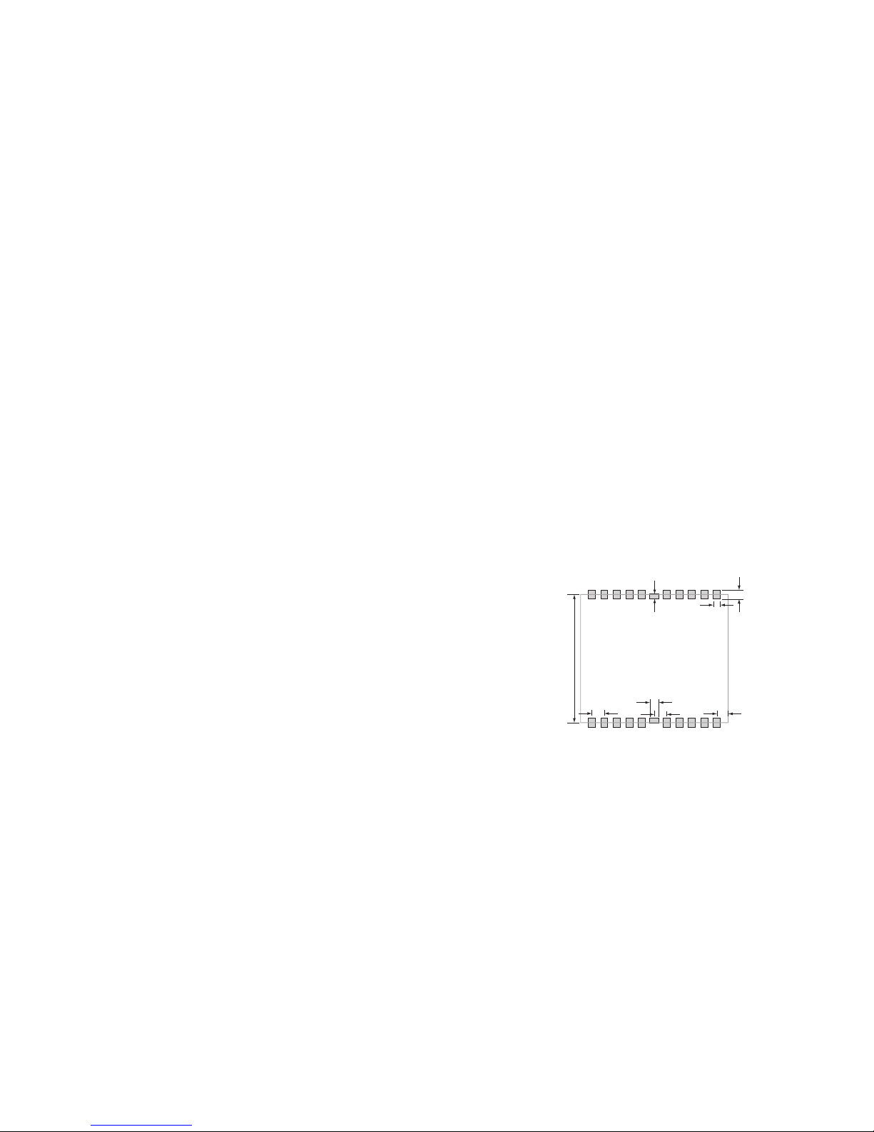
Pad Layout
The pad layout diagram in Figure 31 is designed to facilitate both hand and
automated assembly.
0.028
(0.70)
0.036
(0.92)
0.512
(13.00)
0.050
(1.27)
0.050
(1.27)
0.036
(0.92)
0.020
(0.50)
0.045
(1.15)
Figure 31: Recommended PCB Layout
Page 17
– –
– –
28 29
Microstrip Details
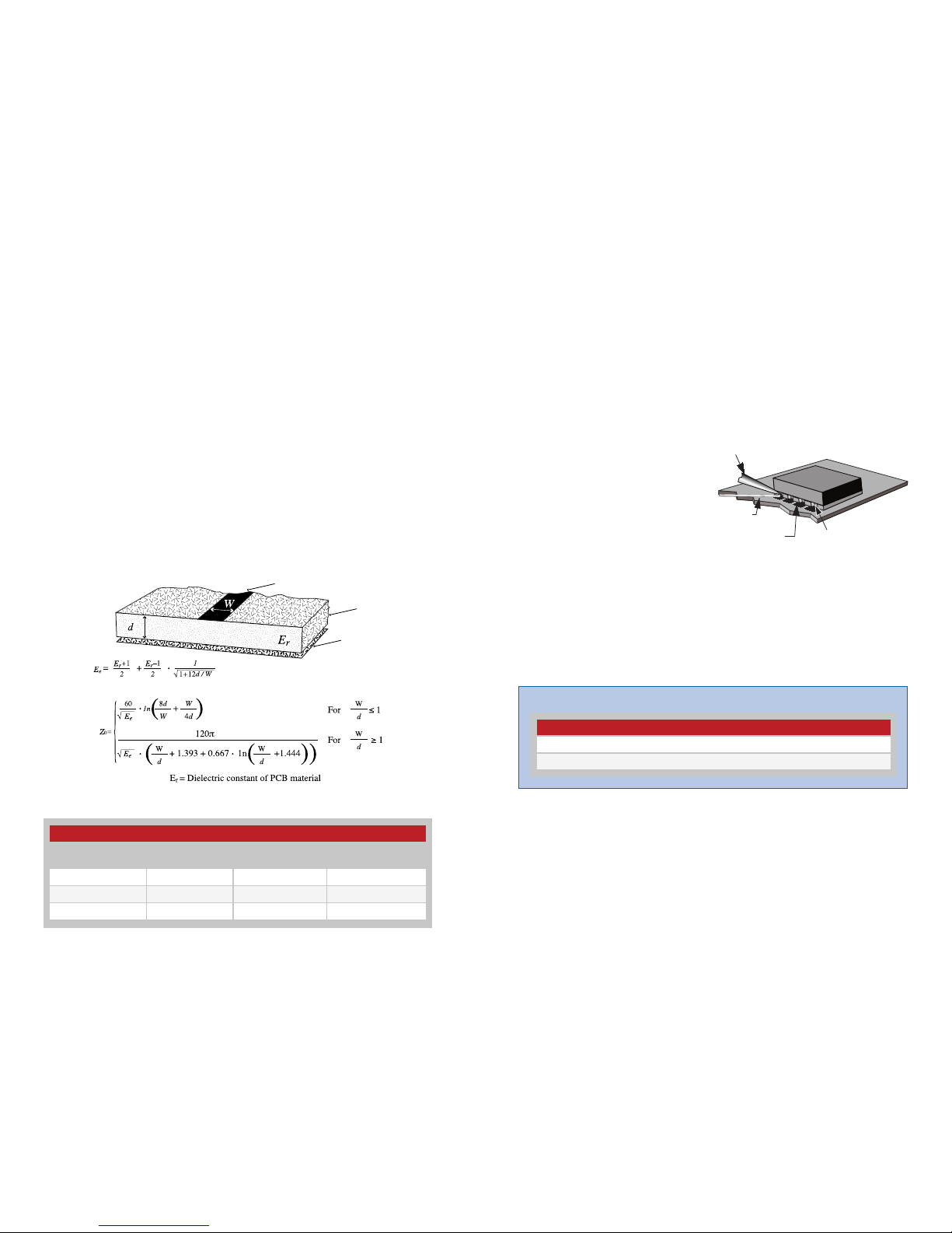
A transmission line is a medium whereby RF energy is transferred from
one place to another with minimal loss. This is a critical factor, especially in
high-frequency products like Linx RF modules, because the trace leading
to the module’s antenna can effectively contribute to the length of the
antenna, changing its resonant bandwidth. In order to minimize loss and
detuning, some form of transmission line between the antenna and the
module should be used unless the antenna can be placed very close (<1⁄8in)
to the module. One common form of transmission line is a coax cable and
another is the microstrip. This term refers to a PCB trace running over a
ground plane that is designed to serve as a transmission line between the
module and the antenna. The width is based on the desired characteristic
impedance of the line, the thickness of the PCB and the dielectric constant
of the board material. For standard 0.062in thick FR-4 board material, the
trace width would be 111 mils. The correct trace width can be calculated
for other widths and materials using the information in Figure 32 and
examples are provided in Figure 33. Software for calculating microstrip lines
is also available on the Linx website.
Trace
Board
Ground plane
Example Microstrip Calculations
Dielectric Constant
Width/Height
Ratio (W/d)
Effective Dielectric
Constant
Characteristic
Impedance (Ω)
4.80 1.8 3.59 50.0
4.00 2.0 3.07 51.0
2.55 3.0 2.12 48.0
Figure 32: Microstrip Formulas
Figure 33: Example Microstrip Calculations
Production Guidelines
The module is housed in a hybrid SMD package that supports hand and
automated assembly techniques. Since the modules contain discrete
components internally, the assembly procedures are critical to ensuring
the reliable function of the modules. The following procedures should be
reviewed with and practiced by all assembly personnel.
Hand Assembly
Pads located on the bottom
of the module are the primary
mounting surface (Figure 34).
Since these pads are inaccessible
during mounting, castellations
that run up the side of the
module have been provided to
facilitate solder wicking to the
module’s underside. This allows
for very quick hand soldering
for prototyping and small volume production. If the recommended pad
guidelines have been followed, the pads will protrude slightly past the
edge of the module. Use a fine soldering tip to heat the board pad and the
castellation, then introduce solder to the pad at the module’s edge. The
solder will wick underneath the module, providing reliable attachment. Tack
one module corner first and then work around the device, taking care not
to exceed the times in Figure 35.
Automated Assembly
For high-volume assembly, the modules are generally auto-placed.
The modules have been designed to maintain compatibility with reflow
processing techniques; however, due to their hybrid nature, certain aspects
of the assembly process are far more critical than for other component
types. Following are brief discussions of the three primary areas where
caution must be observed.
Castellations
PCB Pads
Soldering Iron
Tip
Solder
Figure 34: Soldering Technique
Figure 35: Absolute Maximum Solder Times
Warning: Pay attention to the absolute maximum solder times.
Absolute Maximum Solder Times
Hand Solder Temperature: +427ºC for 10 seconds for lead-free alloys
Reflow Oven: +240°C max (see Figure 36)
Page 18
– –
– –
30 31
Resources
Support
For technical support, product documentation, application notes, regulatory
guidelines and software updates, visit www.linxtechnologies.com
RF Design Services
For customers who need help implementing Linx modules, Linx offers
design services including board layout assistance, programming,
certification advice and packaging design. For more complex RF solutions,
Apex Wireless, a division of Linx Technologies, creates optimized designs
with RF components and firmware selected for the customer’s application.
Call +1 800 736 6677 (+1 541 471 6256 if outside the United States) for
more information.
Antenna Factor Antennas
Linx’s Antenna Factor division has the
industry’s broadest selection of antennas
for a wide variety of applications. For
customers with specialized needs, custom
antennas and design services are available
along with simulations of antenna performance to speed development.
Learn more at www.linxtechnologies.com.
by
Reflow Temperature Profile
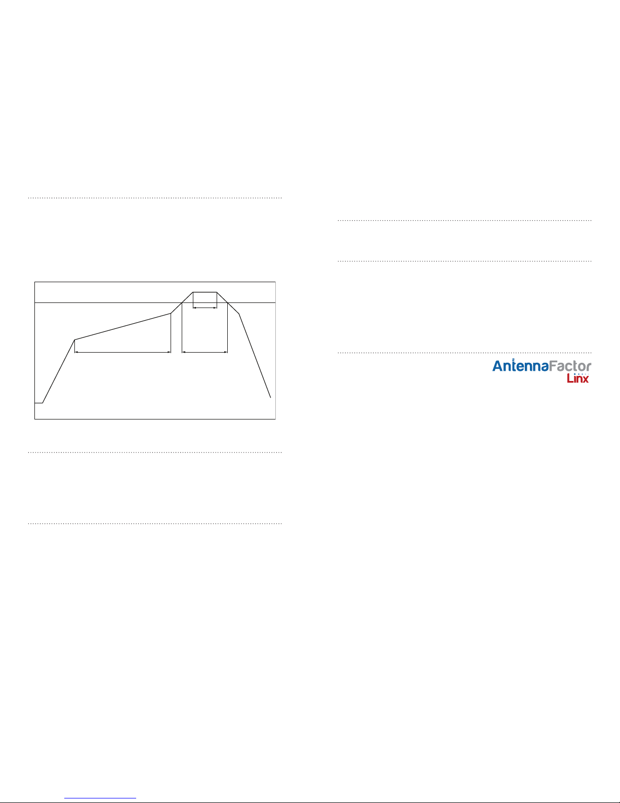
The single most critical stage in the automated assembly process is the
reflow stage. The reflow profile in Figure 36 should not be exceeded
because excessive temperatures or transport times during reflow will
irreparably damage the modules. Assembly personnel need to pay careful
attention to the oven’s profile to ensure that it meets the requirements
necessary to successfully reflow all components while still remaining
within the limits mandated by the modules. The figure below shows the
recommended reflow oven profile for the modules.
Shock During Reflow Transport
Since some internal module components may reflow along with the
components placed on the board being assembled, it is imperative that
the modules not be subjected to shock or vibration during the time solder
is liquid. Should a shock be applied, some internal components could be
lifted from their pads, causing the module to not function properly.
Washability
The modules are wash-resistant, but are not hermetically sealed. Linx
recommends wash-free manufacturing; however, the modules can be
subjected to a wash cycle provided that a drying time is allowed prior
to applying electrical power to the modules. The drying time should be
sufficient to allow any moisture that may have migrated into the module
to evaporate, thus eliminating the potential for shorting damage during
power-up or testing. If the wash contains contaminants, the performance
may be adversely affected, even after drying.
Preheat:
150 - 200°C
Peak: 240+0/-5°C
25 - 35sec
220°C
2 - 4°C/sec
120 - 150sec
2 - 3°C/sec
60 - 80sec
30°C
Figure 36: Maximum Reflow Temperature Profile
Page 19

Disclaimer
Linx Technologies is continually striving to improve the quality and function of its products. For this reason, we
reserve the right to make changes to our products without notice. The information contained in this Data Guide
is believed to be accurate as of the time of publication. Specifications are based on representative lot samples.
Values may vary from lot-to-lot and are not guaranteed. “Typical” parameters can and do vary over lots and
application. Linx Technologies makes no guarantee, warranty, or representation regarding the suitability of any
product for use in any specific application. It is the customer’s responsibility to verify the suitability of the part for
the intended application. NO LINX PRODUCT IS INTENDED FOR USE IN ANY APPLICATION WHERE THE SAFETY
OF LIFE OR PROPERTY IS AT RISK.
Linx Technologies DISCLAIMS ALL WARRANTIES OF MERCHANTABILITY AND FITNESS FOR A PARTICULAR
PURPOSE. IN NO EVENT SHALL LINX TECHNOLOGIES BE LIABLE FOR ANY OF CUSTOMER’S INCIDENTAL OR
CONSEQUENTIAL DAMAGES ARISING IN ANY WAY FROM ANY DEFECTIVE OR NON-CONFORMING PRODUCTS
OR FOR ANY OTHER BREACH OF CONTRACT BY LINX TECHNOLOGIES. The limitations on Linx Technologies’
liability are applicable to any and all claims or theories of recovery asserted by Customer, including, without
limitation, breach of contract, breach of warranty, strict liability, or negligence. Customer assumes all liability
(including, without limitation, liability for injury to person or property, economic loss, or business interruption) for
all claims, including claims from third parties, arising from the use of the Products. The Customer will indemnify,
defend, protect, and hold harmless Linx Technologies and its officers, employees, subsidiaries, affiliates,
distributors, and representatives from and against all claims, damages, actions, suits, proceedings, demands,
assessments, adjustments, costs, and expenses incurred by Linx Technologies as a result of or arising from any
Products sold by Linx Technologies to Customer. Under no conditions will Linx Technologies be responsible for
losses arising from the use or failure of the device in any application, other than the repair, replacement, or refund
limited to the original product purchase price. Devices described in this publication may contain proprietary,
patented, or copyrighted techniques, components, or materials. Under no circumstances shall any user be
conveyed any license or right to the use or ownership of such items.
©2016 Linx Technologies. All rights reserved.
The stylized Linx logo, Wireless Made Simple, WiSE, CipherLinx and the stylized CL logo are trademarks of Linx Technologies.
Linx Technologies
159 Ort Lane
Merlin, OR, US 97532
Phone: +1 541 471 6256
Fax: +1 541 471 6251
www.linxtechnologies.com
 Loading...