

Page 1

NT Series
Master Development System
User's Guide
Page 2

A large-print version of this document is available at
www.linxtechnologies.com.
Page 3

Table of Contents
1 Introduction
2 Ordering Information
2 NT Series Transceiver Development Board
2 Board Objects
3 Initial Setup
3 Troubleshooting
4 The Prototyping Area
5 The TX Power Select Switch
5 The Transceiver Area
6 The Power Area
6 The Evaluation Area
8 The Range Test Area
9 The PC Control Area
10 The PC Software
13 Using the Boards as a Design Reference
13 About Antennas
14 Board Control
14 Transmitter Output Power Selection
15 Transceiver Area
15 Header Section
16 Range Test Area
16 Power Area
17 Evaluation Area
17 LEDs
18 Single Routing
19 Online Resources
Page 4

Page 5
– –
Introduction
The Linx NT Series RF transceiver modules offer a simple, efficient and
cost-effective method of adding wireless communication capabilities
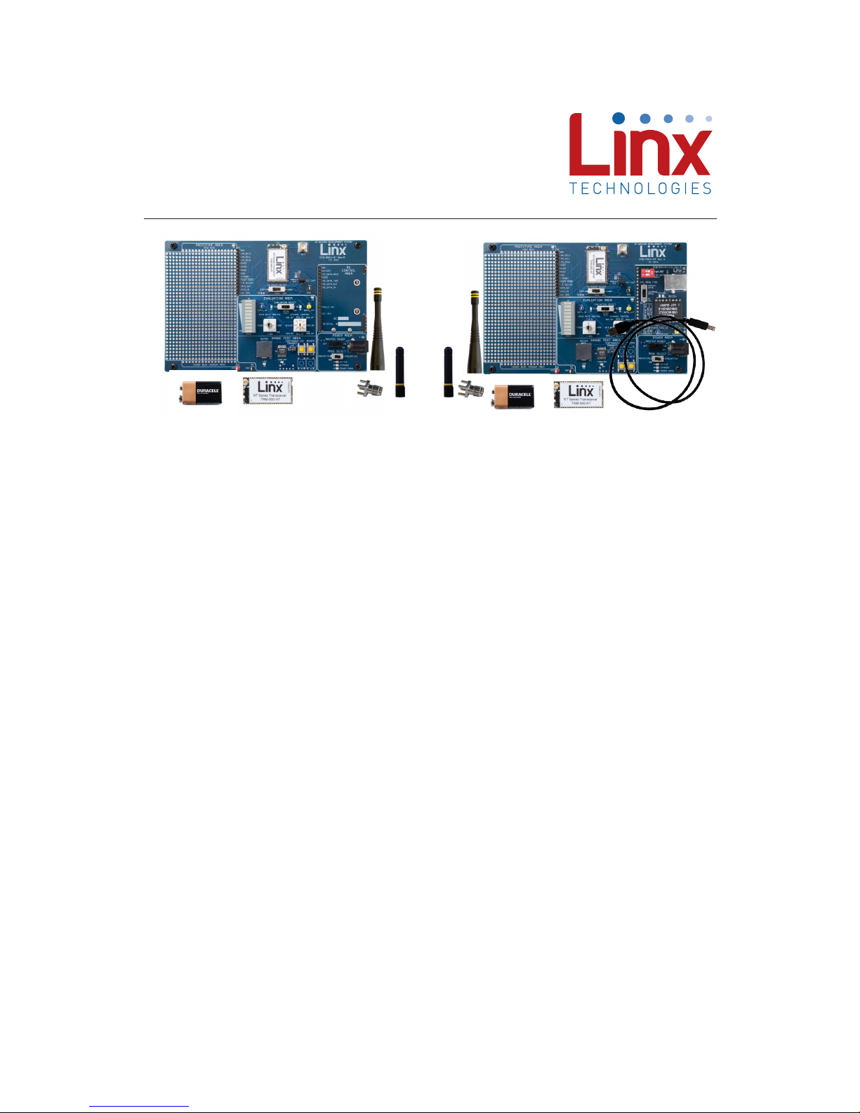
to any product. The Master Development System (Figure 1) provides a
designer with all the tools necessary to correctly and legally incorporate
the NT Series into an end product. The development boards serve several
important functions:
• Rapid Module Evaluation: The boards allow the performance of the Linx
NT Series modules to be evaluated quickly in a user’s environment.
Using the onboard transcoders, a pair of development boards can be
used to evaluate the range performance of the modules.
• Application Development: An onboard prototyping area allows for the
development of custom circuits directly on the development board. All
signal lines are available on a header for easy access.
• Software Development: A PC interface allows for development and
testing of custom software applications for control of the module.
• Design Benchmark: The boards provide a known benchmark against
which the performance of a custom design may be judged.
The Master Development System includes two assembled development
boards, four NT Series transceivers*, two CW Series antennas, two 9V
batteries, four reverse polarity SMA connectors*, a USB interface board
and full documentation.
NT Series Master Development System
User's Guide
Figure 1: NT Series Master Development System
* One part is soldered to each board
1
Revised 5/31/2013
Page 6
– –
Board Objects
NT Series Transceiver Development Board
1
2
3
4
5
6
7
8
9
10
11
12
13
14
15
17
16
Ordering Information
Ordering Information
Part Number Description
MDEV-868-NT 868MHz NT Series Master Development System
MDEV-900-NT 900MHz NT Series Master Development System
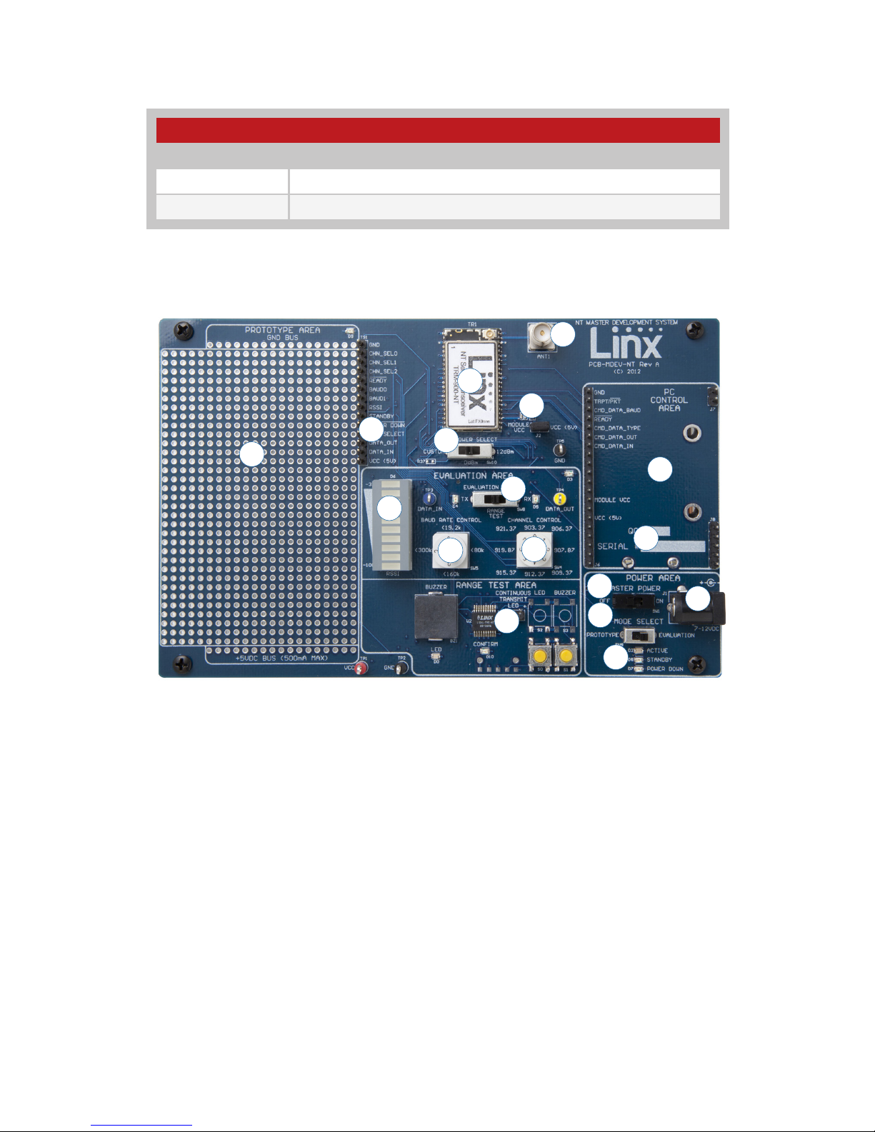
1. Prototype Area
2. Break-Out Header
3. RSSI Level
4. NT Series Transceiver
5. RP-SMA Antenna Connector
6. Module Power Header
7. Output Power Level
Selection Switch
8. Evaluation Selection Switch
9. Baud Rate Selection Dial
10. Channel (Frequency)
Selection Dial
11. Transcoder Range Test Area
12. PC Control Area
13. 9V Battery (on the back of
the board)
14. DC Power Jack
15. Master Power Switch
16. Mode Selection Switch
17. Module Mode Indicator LEDs
Figure 2: Ordering Information
Figure 3: NT Series Transceiver Development Board
2
Page 7

– –
3
Initial Setup
Unpack the development system, attach the antennas and install a 9V
battery on each development board. The boards can be used in two
different configurations: Prototype and Evaluation. The Mode Selection
switch sets the configuration. By default, the boards are set to Range Test
in the Evaluation configuration.
Evaluation Configuration
Setting the Mode Select switch to the EVALUATION (right) position enables
the Evaluation Configuration. In this configuration, the module’s signal lines
are routed to the Evaluation Area for control. This enables the module to be
configured by the controls on the board while allowing custom data to be
sent over the link.
Range Test
The development boards feature an onboard Linx MT Series transcoder
which facilitates range testing. Buttons on one board activate a light or
buzzer on the other. A confirmation LED provides visual acknowledgment
that a transmission was received across the wireless link.
Range Test is part of the Evaluation configuration and is the default
configuration out of the box. To use the boards this way, place the Mode
Select switch to Evaluation and the Evaluation Select switch to the RANGE
TEST (middle) position. This routes the DATA_IN, DATA_OUT and T/R_SEL
lines to the MT Series Transcoder.
Prototype Configuration
Setting the Mode Select switch to the PROTOTYPE (left) position enables
the Prototype Configuration. In the Prototype configuration, the module’s
signal lines are routed to the break-out header next to the Prototype Area.
This allows the module to be controlled with custom application circuitry.
Software Development
The kit includes one USB interface board for connection to a PC. Included
software demonstrates use of the module’s Command Data Interface (CDI).
Troubleshooting
If the boards fail to work out of the box, then try the following:
• Make sure that the Master Power, Mode Select and Evaluation Select
switches are in the correct positions. The Active LED should be on
Page 8
– –
• Make sure that the Baud Rate and Channel switches are set the same
on both boards
• Check that the antennas are connected
• Make sure that a jumper is installed on the Module Power Header
• Make sure that the batteries are not dead
If all of these appear to be in order, please call +1 800 736 6677 or e-mail
[email protected] for technical support.
The Prototyping Area
In addition to its evaluation functions, the board may also be used for
product development. It features a prototyping area to facilitate the addition
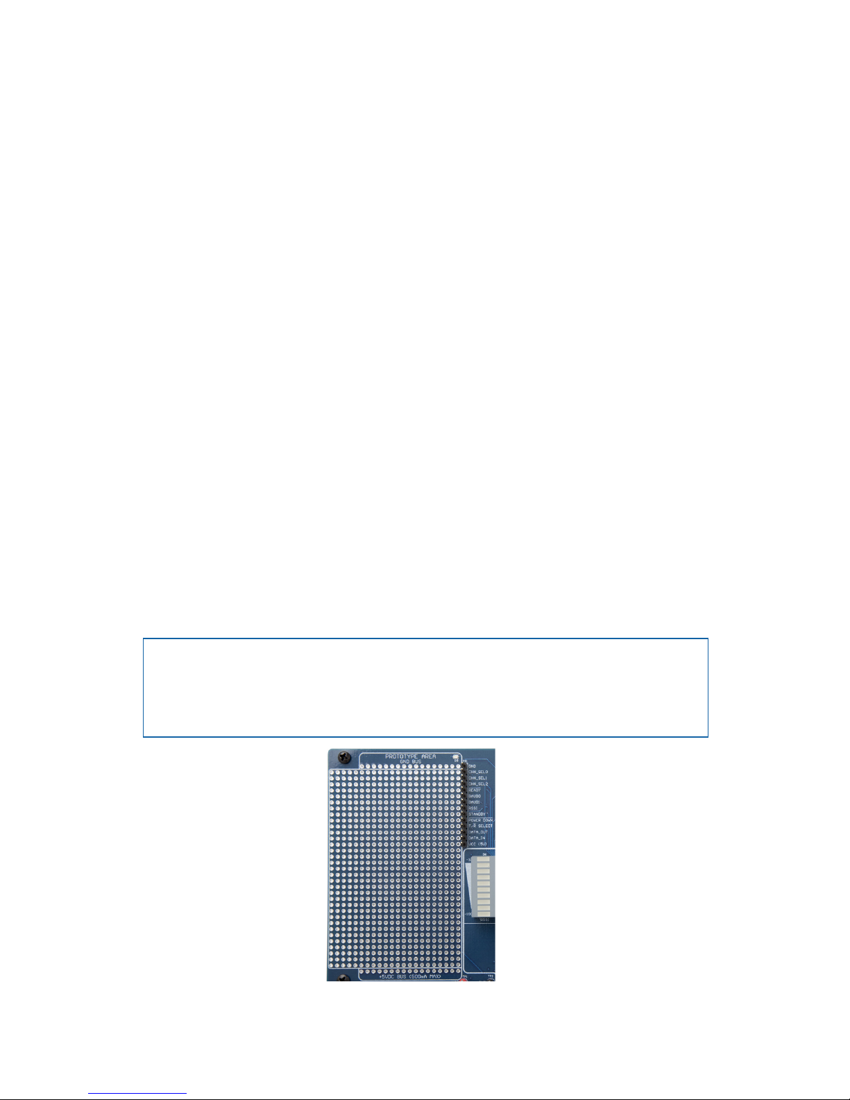
of application-specific circuitry (Figure 4). The prototyping area contains a
large area of plated through-holes so that external circuitry can be placed
on the board. The holes are set at 0.100" on center with a 0.040" diameter,
accommodating most industry-standard SIP and DIP packages.
External circuitry can be easily interfaced to the NT transceiver through the
breakout header (TS1) to the right of the prototyping area. The Mode Select
switch should be set to the left position to enable the module’s lines to
be controlled from the prototyping area. At the bottom of the prototyping
area is a row connected to the 5V power supply and at the top is a row
connected to ground.
Note: The onboard 5-volt regulator has approximately 600mA available
for additional circuitry. If more current is required, the user must add an
additional regulator or power the board from an external supply.
Figure 4: The Development Board
Prototyping Area
4
Page 9
– –
5
The TX Power Select Switch
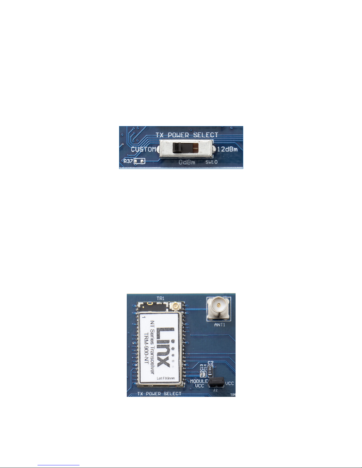
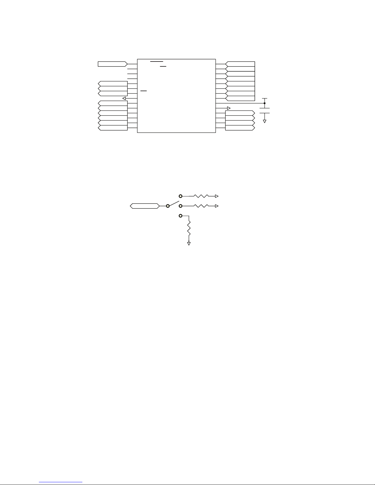
The board has a switch to select among three different transmitter output
power levels (Figure 5). The right position sets the module to full power of
about 12dBm. The center position sets the output power to about 0dBm,
which is the legal limit for most applications. The left position uses resistor
R37 to set the power. This position is an unpopulated 0603 size resistor
location. A resistor can be placed here to set the output power to any
available level. Please see the NT Series Data Guide for more information
on resistor values. A power cycle is required for changes to take effect.
The Transceiver Area
The transceiver section consists of the transceiver module and a reversepolarity SMA connector as shown in Figure 6. The RP-SMA connector
is FCC compliant and reverses the center pin and socket. RP-SMA
connectors will mate with but not provide electrical connection to standard
SMA connectors or SMA equipped antennas. A header next to the module
disconnects the module’s power from the main board power. This can
be used for current measurements or to power the module alone from an
external power source. A jumper must be installed to power the module
from the board.
Figure 5: The Development Board TX Power Select Switch
Figure 6: The Development Board Transceiver Area
Page 10
– –
6
The Power Area
The Power Area has two switches that control power to the board and the
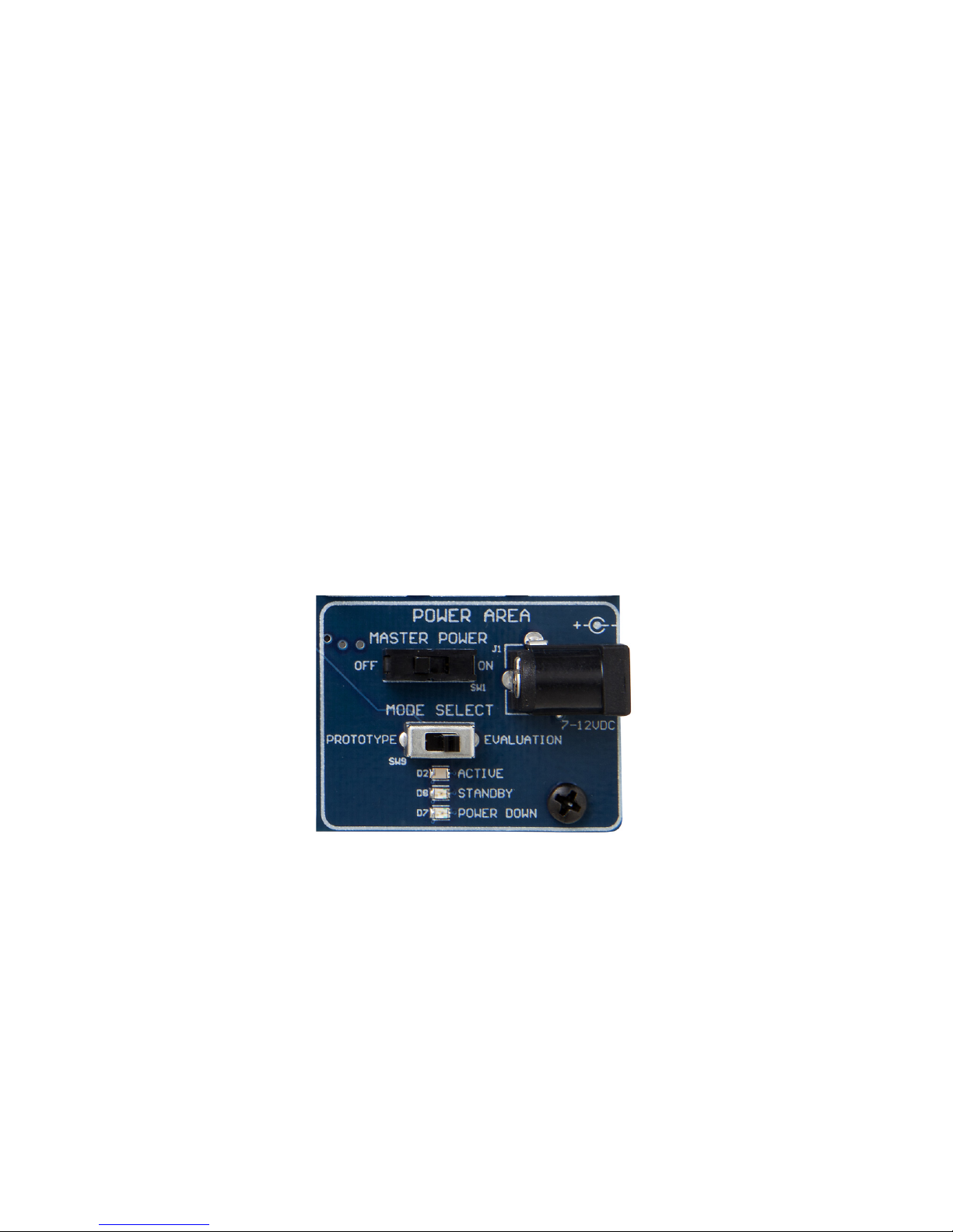
type of operation (Figure 7). The Master Power switch supplies power from
the 9V battery or the power jack to the board. The power jack accepts a
2.5mm plug with the tip ground and the shell 7 to 12VDC.
The Mode Select switch configures the board for either Prototype operation
(left position) or Evaluation operation (right position). In Prototype operation,
the module’s signal lines are routed to the header next to the Prototype
Area. This allows custom circuits to easily interface with the module.
In Evaluation operation, the module’s signal lines are routed to the
Evaluation Area. The controls in this area allow the module to be operated
without any other circuits, microcontrollers or a PC.
Three LEDs show the state of the module. Active shows the module is
on and ready for operation. Standby and Power Down indicate that the
low power modes have been entered and the module is not ready for
operation.
The Evaluation Area
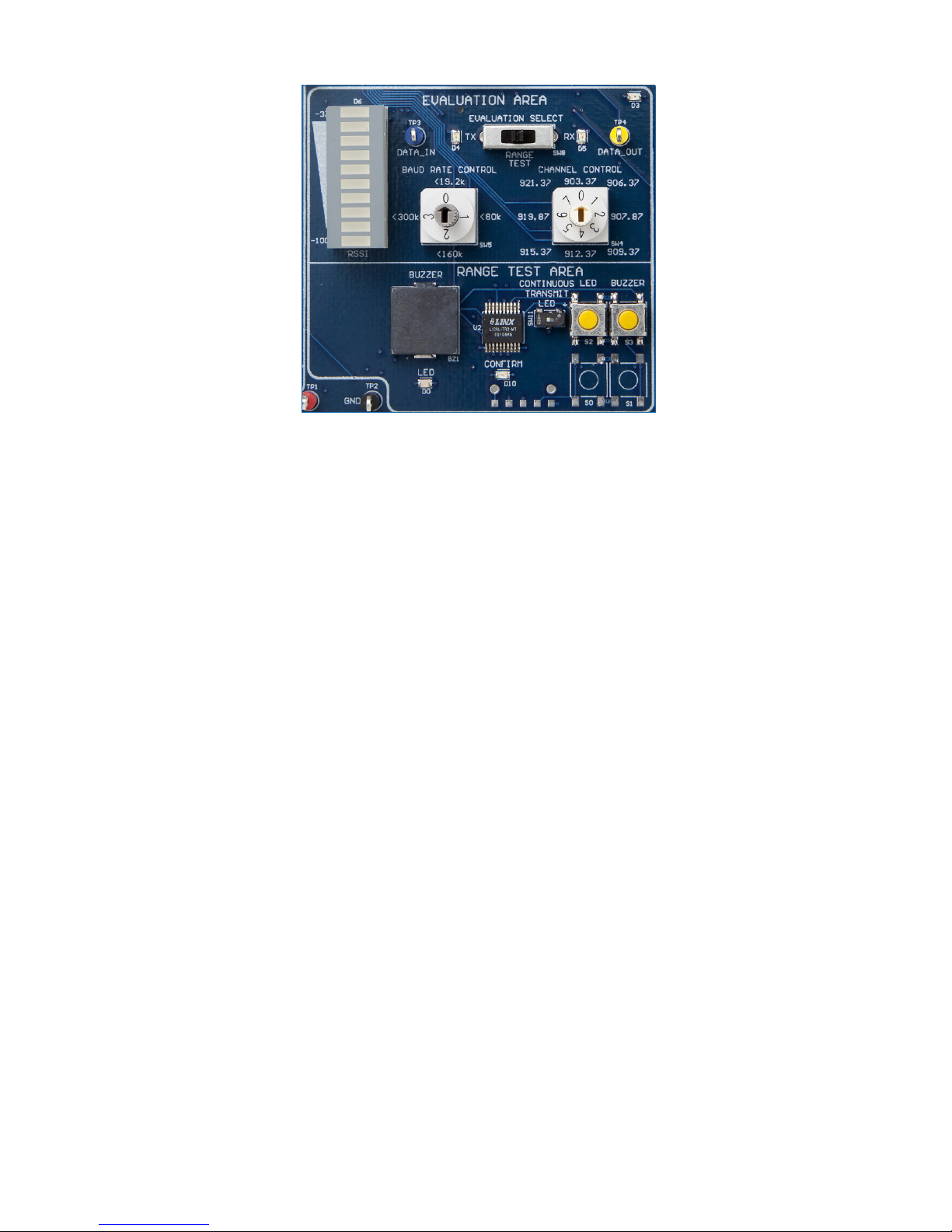
The Evaluation Area is activated by setting the Mode Select switch to the
right position. Figure 8 shows the Evaluation Area.
The Evaluation Select switch configures the area for different types of
evaluation. The left position puts the module into transmit mode.
The orange TX LED lights up and any data present on the blue DATA_IN
test point is transmitted by the module.
Figure 7: The Development Board Power Area
Page 11
– –
7
The right position puts the module into receive mode. The yellow RX LED
lights up and data received by the module is output on the yellow
DATA_OUT test point.
These two configurations allow the module to transmit and receive custom
data while controlling the baud band and channel with the frequency dials
on the board. It is similar to the Prototype Area, but requires less external
circuitry to configure the module. The switches on the board are used for
hardware configuration in this mode.
The Baud Rate Control dial sets the BAUD0 and BAUD1 lines to configure
the module’s baud band. This should be set the same on both boards for
proper operation.
The Channel Control dial sets the CHAN_SEL0, CHAN_SEL1 and
CHAN_SEL2 lines to configure the module’s channel. This should be set
the same on both boards for proper operation.
An LED bar is used to provide a general indication of the RF signal
strength. The closer the active LED is to the top, the stronger the received
signal level. The receiver must be active for at least one second for the
RSSI level to update.
The center position on the Evaluation Select switch activates the Range
Test Area, allowing the link’s range to be evaluated. This area is described
in detail in the Range Test Area section of this user’s guide.
Figure 8: The Development Board Level Adjust Section
Page 12
– –
8
The Range Test Area
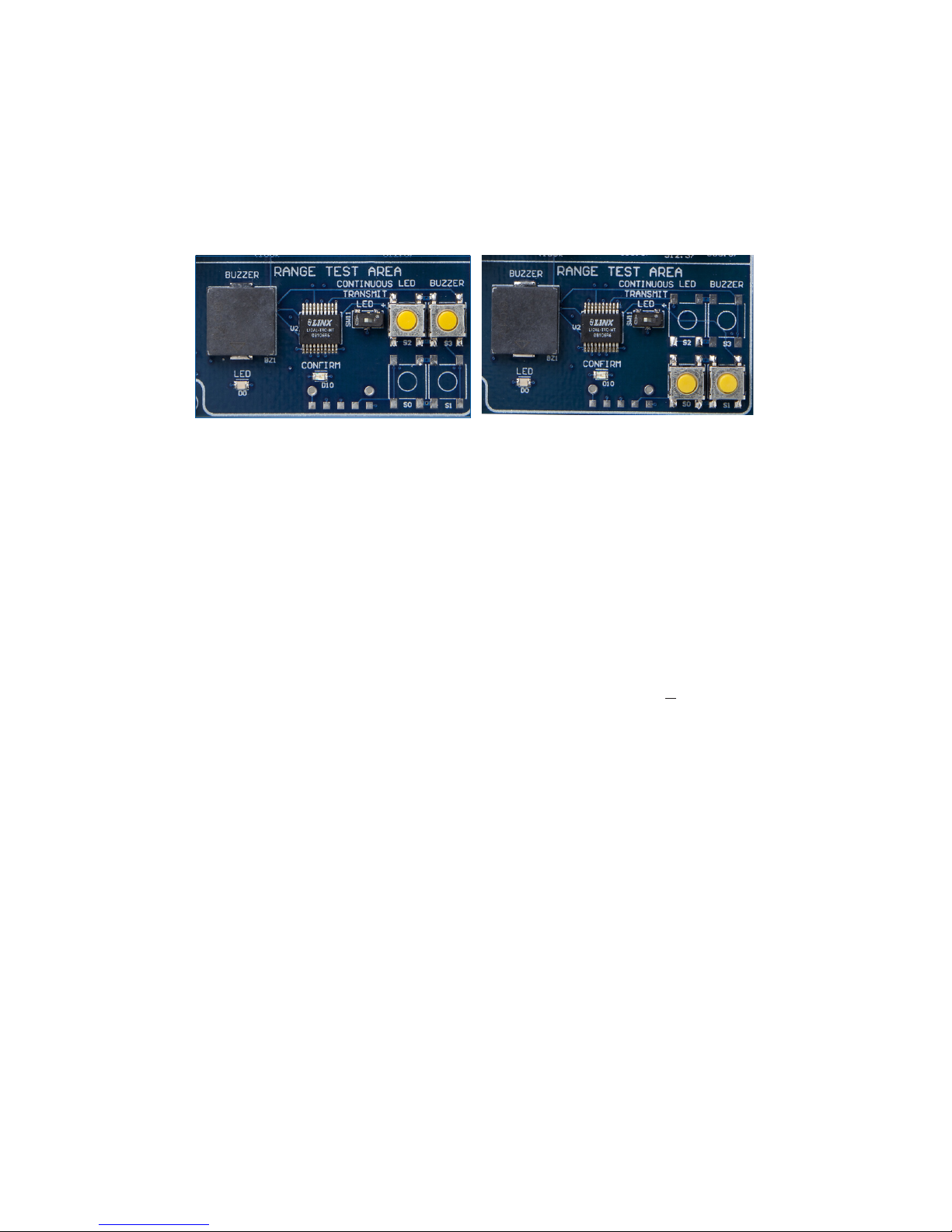
The board features an MT Series remote control transcoder with two push
buttons, a buzzer and an LED. The two boards in the kit are populated
differently so that the button inputs on one board are outputs on the other
board. Figure 9 shows the differences.
When a button is pressed on one board, the status of both buttons is
captured, encoded into a data stream, and transmitted. The data
recovered by the receiving board is decoded and the transcoder’s data
lines are set to replicate the states of the buttons, driving either the buzzer
or the LED. A confirmation packet is then sent to the transmitting board
activating the Confirm LED.
To activate this area of the board, the module’s DATA and T/R_SEL lines
must be routed to the transcoder. This is accomplished by setting the
Mode Select switch to the right position and the Evaluation Select switch to
the middle position.
After the boards have been configured, place Board A on a flat surface
and turn it on. Turn on Board B and press button S1. The buzzer on Board
A will sound and the Confirm LED on Board B will light up. The usable
range of the link in your environment can be ascertained by carrying Board
B away from Board A. Switch SW11 has been provided to continuously
transmit the LED activation without having to hold down a button.
As you near the maximum range of the link in your area, it is common for
the signal to cut in and out as you move. This is normal and can result from
other interfering sources or fluctuating signal levels due to multipath effects.
The areas in which this occurs are commonly called “nulls” and simply
walking a little farther will often restore the signal.
Figure 9: The Development Board Range Test Section
Board A Board B
Page 13
– –
To achieve maximum range, keep objects such as your hand away
from the antennas and ensure that the antennas on the boards have
an unobstructed line-of-sight path to each other. Range performance is
determined by many interdependent factors. If the range you are able to
achieve is significantly less than specified by Linx for the products you are
testing, then there is likely a problem with either the board or the ambient
RF environment in which the board is operating. First, check the battery,
switch positions, TX output power setting and antenna connection.
Check the range performance on different channels. Next, measure the
receiver’s RSSI voltage with the transmitter turned off to determine if
ambient interference is present. If this fails to resolve the issue, please
contact Linx technical support.
The PC Control Area
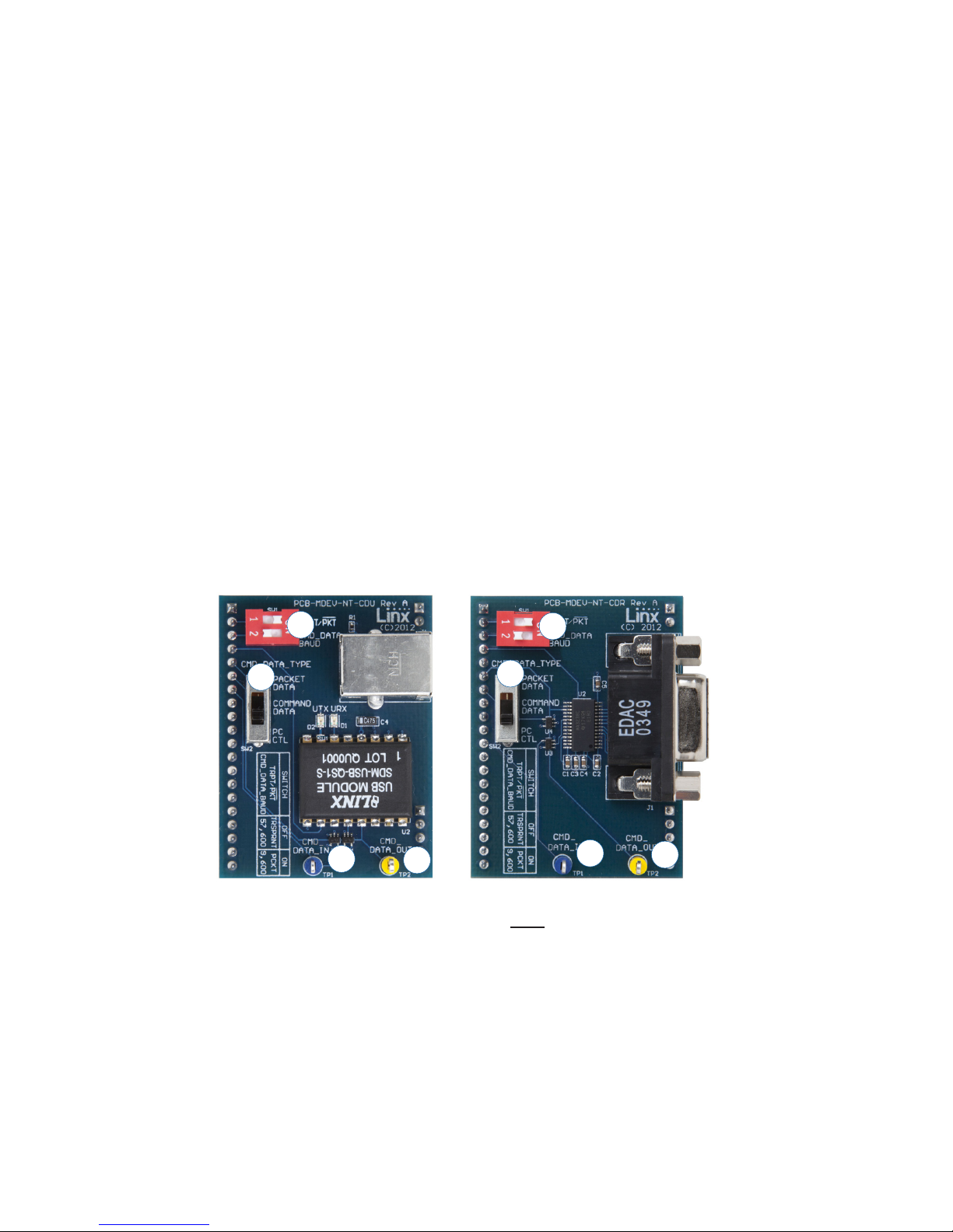
The PC Control Area is used with a daughter board to connect the
module’s Command Data Interface to a PC. This advanced feature is a
serial data interface for configuration and data transfer. One USB interface
board is included with the development kit. Additional USB interface boards
or an RS-232 interface board can be purchased separately.
The top DIP switch (1) controls the TRPT/PKT line on the module. This
line selects between transparent data transmission and packet data
transmission. Slide it to the left for transparent data and to the right for
packet data.
The bottom DIP switch (1) controls the CMD_DATA_BAUD line on
the module. This is the data rate for the CDI and has no effect on the
over-the-air data rate. Slide to the left for 57,600bps and to the right for
9,600bps.
9
Figure 10: PC Interface Boards
1
2
3
4
1
3
4
2
Page 14
– –
The three position slide switch (2) controls the CMD_DATA_TYPE line. This
line tells the module that the data coming in on the CDI is either command
data for configuring the module (middle position) or packet data to be
transmitted over the air (top position). The bottom position connects this
line to the DTR line on the USB or RS-232 interface. This allows the PC
software to control the line, giving it the ability to configure the module and
send data.
Test points for CMD_DATA_IN (3) and CMD_DATA_OUT (4) are provided so
that the communications can be monitored.
The PC Software
The kit includes PC software that can be used to configure the module
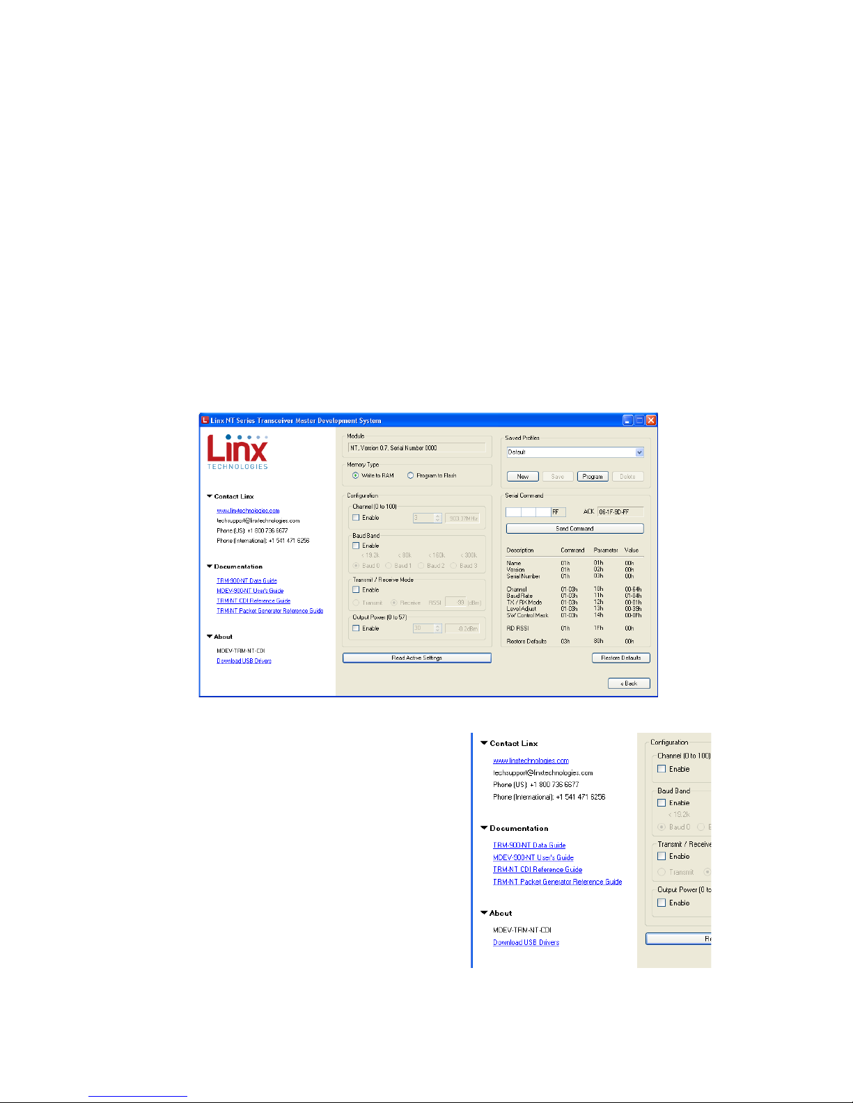
through the PC interface daughter board. Figure 11 shows the software.
The left side of the window contains
labels that expand to show links to useful
information (Figure 12). This includes the
Linx Technologies contact information
and links to the website for the latest
product documentation and software
updates. Clicking on these links opens
the page in the computer’s default web
browser.
Figure 11: Development Kit PC Software
Figure 12: Development Kit PC Software
10
Page 15
– –
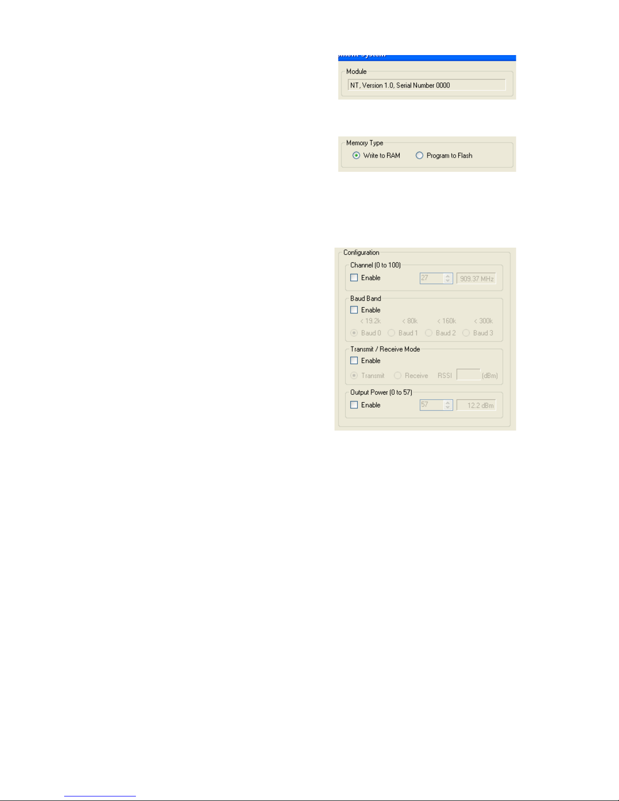
The command portion of the window
starts in the middle of the window (Figure
13). At the top is a box that states the
product name, firmware version and
serial number.
Below this is a selection that determines
how the module is configured (Figure 14).
Writing to RAM is faster, but the settings
are lost when power is cycled to the module. Programming to flash takes a
bit longer (5ms/byte), but the settings are retained when power is cycled to
the module.
Below this are the configuration settings
(Figure 15). These allow the software to
change the channel, baud band, transmit
and receive mode and the output
power. By default the module looks to
its hardware pins for these configuration
settings, so software control must be
enabled for it to take control. This is
done by checking the Enable checkbox
in each section.
The Channel configuration allows the
user to select from among all 101 channels offered by the module rather
than just the eight available with the hardware lines. A selection box shows
the channel and a text box shows the channel’s frequency.
The Baud Band setting adjusts internal filters and other settings to set
the transceiver’s maximum over-the-air data rate. The Baud Band section
allows for the selection from among the four baud bands.
The Transmit/Receive Mode selection activates the transceiver’s transmitter
or receiver. When the receiver is active the measured RSSI level is shown in
the text box.
The Output Power section allows the module’s transmitter output power
level to be adjusted. The NT Series has 57 power levels that drop the
power in approximately 0.5dB increments. The adjacent text box shows
the approximate power. This is not a measured value, but an approximate
value based on characterization of the modules.
11
Figure 13: Development Kit PC Software
Figure 14: Development Kit PC Software
Figure 15: Development Kit PC Software
Page 16
– –
12
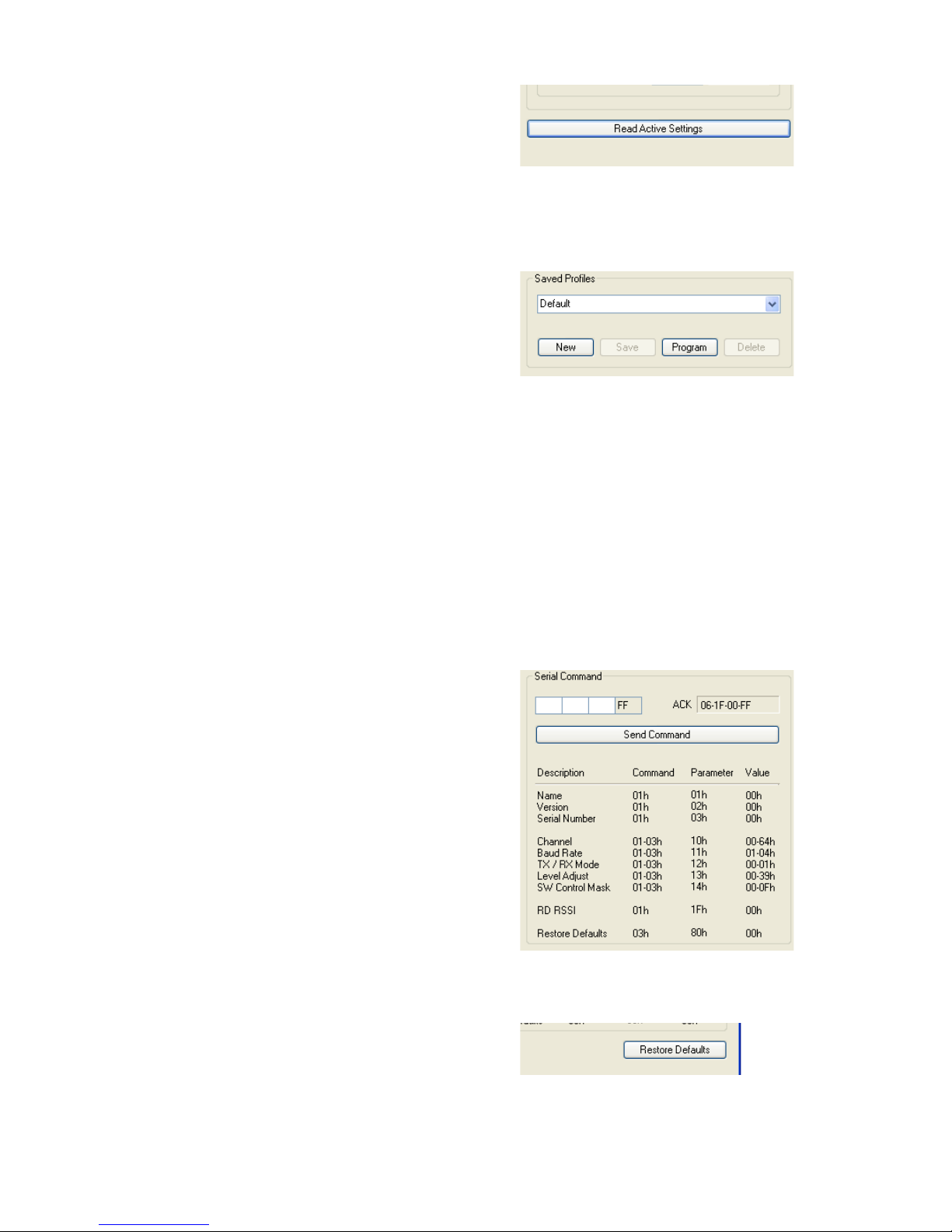
The “Read Active Settings” button
at the bottom (Figure 16) reads the
existing configuration settings from the
module and adjusts the values in the
configuration sections based on the
module’s current configuration.
The right column in the window starts
with the Profile section (Figure 17).
Specific configuration settings can be
saved as a profile and loaded into a
connected module. This allows the
software to be used in small-scale
production lines for products that provide
connection to the CDI.
Select the “New” button to create a new profile and give it a name. Set
the configuration controls as desired and click the “Save” button to save
the profile. Click the “Program” button to send the profile to the module.
All of the profiles saved on the PC can be viewed in the drop down menu
and sent to the module with the “Program” button. The “Delete” button
removes the selected profile from the computer.
The Serial Command section (Figure 18)
provides the ability to send a specific
packet to the module. Byte values are
typed into the boxes to create the packet
and the “Send Command” button sends
the packet to the module. The ACK text
box displays the module’s response. The
possible values for each byte are shown
in the table below the “Send Command”
button.
The “Restore Defaults” button (Figure 19)
writes the factory default values to the
transceiver. This is an easy way to restore
the module to a known configuration.
Figure 16: Development Kit PC Software
Figure 17: Development Kit PC Software
Figure 18: Development Kit PC Software
Figure 19: Development Kit PC Software
Page 17

– –
13
Using the Boards as a Design Reference
From a layout perspective, the master development boards included in this
kit are quite simple, yet they illustrate some important techniques that can
be incorporated into a design. The module’s mounting pads extend slightly
past the edge of the part. This eases hand assembly and allows for better
heat conduction under the part if rework is necessary. The use of a full
ground plane fill on the lower side of the board serves three important
purposes.
First, since a ¼-wave antenna is employed, the ground plane is critical to
serve as a counterpoise. Application Note AN-00500 and AN-00501
provide additional details on how a ground plane affects antenna function.
Second, a ground plane suppresses the transfer of noise between stages
of a product as well as unintentional radiation of noise into free space.
Third, a ground plane allows for the implementation of a microstrip feed
to the antenna. The term microstrip refers to a PCB trace running over
a ground plane that is designed to serve as a 50-ohm transmission line
between the module and the antenna. A microstrip is implemented on this
evaluation board. The module’s data guide and a calculator available on the
Linx Technologies website provide more information on the microstrip
implementation and calculations.
About Antennas
The choice of antennas is one of the most critical and often overlooked
design considerations. The range, performance and legality of an RF link
are critically dependent upon the type of antenna employed. Linx offers a
variety of antenna styles that may be considered for a design. Included with
the development system is a Linx CW Series connectorized whip antenna
that should be connected prior to using the kit. Despite the fact that the
antenna is not centered on the board’s ground plane, it exhibits a VSWR of
<1.7 and demonstrates the module’s best practical performance.
Page 18
– –
BOARD CONTROL
MODE_SEL
TX_SEL
RNG_SEL
RX_SELCH_BD_CTL
PDN
RX_LED
STDBY
ACTV_LED
PDN_LED
STBY_LED
DACOUT/AN2/RA2
4
AN3/RA3
5
RA4
6
SS/AN4/RA5
7
VSS
8
OSC1/RA7
9
OSC2/RA6
10
RC0
11
RC1
12
RC2
13
RA0/AN0/SS
2
RA1/AN1
3
RB3/AN9
24
RB4/AN11
25
RB5/AN13
26
RB6/PGC
27
20
RB0/AN12/INT
21
RB1/AN10
22
RB2/AN8
23
RX/RC7
18
19
RB7/PGD
28
RE3/MCLR/VPP
1
SCL/SCK/RC3
14
SDA/SDI/RC4
15
SDO/RC5
16
TX/RC6
17
U11
PIC16F1938
GND
VCC
PGC
PGDVPP
C7
0.1uF
GND
VDD
VSS
R2097.6k 1%
LADJ
R30 NS/DNP
GND
GND
SW10
R37
NS/DNP
GND
Transmitter Output Power Selection
BOARD CONTROL
MODE_SEL
TX_SEL
RNG_SEL
RX_SELCH_BD_CTL
ALL_EN
TR_CTL1
TR_CTL2
DATA_CTL1
DATA_CTL2
PROTO_LED
PDN
TX_LED
RX_LED
STDBY
ACTV_LED
PDN_LED
STBY_LED
GND
DACOUT/AN2/RA2
4
AN3/RA3
5
RA4
6
SS/AN4/RA5
7
VSS
8
OSC1/RA7
9
OSC2/RA6
10
RC0
11
RC1
12
RC2
13
RA0/AN0/SS
2
RA1/AN1
3
RB3/AN9
24
RB4/AN11
25
RB5/AN13
26
RB6/PGC
27
20
RB0/AN12/INT
21
RB1/AN10
22
RB2/AN8
23
RX/RC7
18
19
RB7/PGD
28
RE3/MCLR/VPP
1
SCL/SCK/RC3
14
SDA/SDI/RC4
15
SDO/RC5
16
TX/RC6
17
U11
PIC16F1938
GND
VCC
PGC
PGDVPP
C7
0.1uF
GND
EVAL_LED
VDD
VSS
Board Control
Figure 20: Board Control
14
Figure 21: Transmitter Output Power Selection
Page 19
– –
15
Transceiver Area
1
2
J2
VCCM
VCC
IN
1
VCC
2
GND3NC
COM
NO
U4
MAX4544EUT
T/R_SEL_R
GND
VCC
GND
LED
GREEN
R18
620
D0
LED-0805-GRN
B
3
A`
2
A
1
F`
12
F
13
VCC
14
U3
R16
100K
R17
TRANSCEIVER AREA RANGE TEST AREA
D10
GND
GND
GND
T/R_SEL_R
DATA_MT
GND
GND
GND
R8
100K
R9
100K
R10
100K
R11
100K
R12
100K
BLUE
R13
200 ohm
VCC
SW-SMT-SPDT
VCC
GND GND
GND
GNDGND
GNDGND
VCCM
BAUD1
RSSI
STDBY
CD_IN
CD_OUT
CD_TYPE
CD_BAUD
DATA_OUT
DATA_IN
PDN
CS1
CS2
LADJ
RDY
T/R_SEL
BAUD0
CS0
TRPT/PKT
RF
1
GND
2-5
ANT1
CONREVSMA001
GND
GND
GND
GND
GND GND
R21
100K
R22
100K
NC0
NC
2
GND
3
NC
4
NC
5
GND
6
NC
7
TRPT/PKT
9
CHN_SEL0
10
GND
11
T/R_SEL
18
BAUD0
19
RSSI
21
GND
22
GND
23
POWER_DOWN
24
VCC
25
STANDBY
26
CMD_DATA_IN
27
CHN_SEL1
12
GND
17
CHN_SEL2
13
LVL_ADJ
14
READY
15
NC
16
NC
8
BAUD1
20
GND
1
GND
28
CMD_DATA_OUT
29
CMD_DATA_TYPE
30
CMD_DATA_BAUD
31
NC
32
NC
33
GND
34
NC
35
NC
36
DATA_OUT
37
DATA_IN
38
GND
39
NC
40
NC
41
GND
42
ANTENNA
43
GND
44
TR1
TRM-XXX-NT
VCC2
VCC2
R36
100K
VCC
R35
2.2K
GND
C13
0.01uF
C14
100pF
GND GND
R43
100K
VCC2
Header Section
1
2
J2
VCCM
VCC
IN
1
VCC
2
GND
3
U4
MAX4544EUT
T/R_SEL_R
GND
VCC
GND
LED
GREEN
R18
620
D0
LED-0805-GRN
GND
B`
4
C
5
C`
6
GND
7
B
3
A`
2
A
1
VCC
U3
CD4069UB
R16
100K
R17
10k
C4
0.01uF
TRANSCEIVER AREA RANGE TEST AREA
J1
PWRJACK
D1
B1
SW1
HEADER SECTION
GND 1
2
J7
GND
GND
CD_IN
CD_OUT
CD_BAUD
TRPT/PKT
1
2
3
4
5
6
7
8
9
10
11
12
13
14
15
16
17
18
19
20
J6
CD_TYPE
VCC
GND
1
2
3
4
5
J8
D10
GND
GND
GND
GND
GND
GND
R8
100K
R9
100K
R10
100K
R11
100K
R12
100K
BLUE
R13
200 ohm
VCC2
RDY
VCC
GND
DATA_OUT_P
DATA_IN_P
RDY
T/R_SEL_P
PDN
STDBY
CS0_P
CS1_P
CS2_P
BAUD0_P
BAUD1_P
1
2
3
4
5
6
7
8
9
10
11
12
13
14
TS1
RSSI_P
GND GND
GND
GNDGND
GNDGND
VCCM
BAUD1
RSSI
STDBY
CD_IN
CD_OUT
CD_TYPE
CD_BAUD
DATA_OUT
DATA_IN
PDN
CS1
CS2
LADJ
RDY
T/R_SEL
BAUD0
CS0
TRPT/PKT
RF
1
GND
2-5
ANT1
CONREVSMA001
GND
GND
GND
GND
GND GND
R21
100K
R22
100K
NC0
NC
2
GND
3
NC
4
NC
5
GND
6
NC
7
TRPT/PKT
9
CHN_SEL0
10
GND
11
T/R_SEL
18
BAUD0
19
RSSI
21
GND
22
GND
23
POWER_DOWN
24
VCC
25
STANDBY
26
CMD_DATA_IN
27
CHN_SEL1
12
GND
17
CHN_SEL2
13
LVL_ADJ
14
READY
15
NC
16
NC
8
BAUD1
20
GND
1
GND
28
CMD_DATA_OUT
29
CMD_DATA_TYPE
30
CMD_DATA_BAUD
31
NC
32
NC
33
GND
34
NC
35
NC
36
DATA_OUT
37
DATA_IN
38
GND
39
NC
40
NC
41
GND
42
ANTENNA
43
GND
44
TR1
TRM-XXX-NT
VCC2
VCC2
R36
100K
VCC
R35
2.2K
GND
C13
0.01uF
C14
100pF
GND GND
R43
100K
VCC2
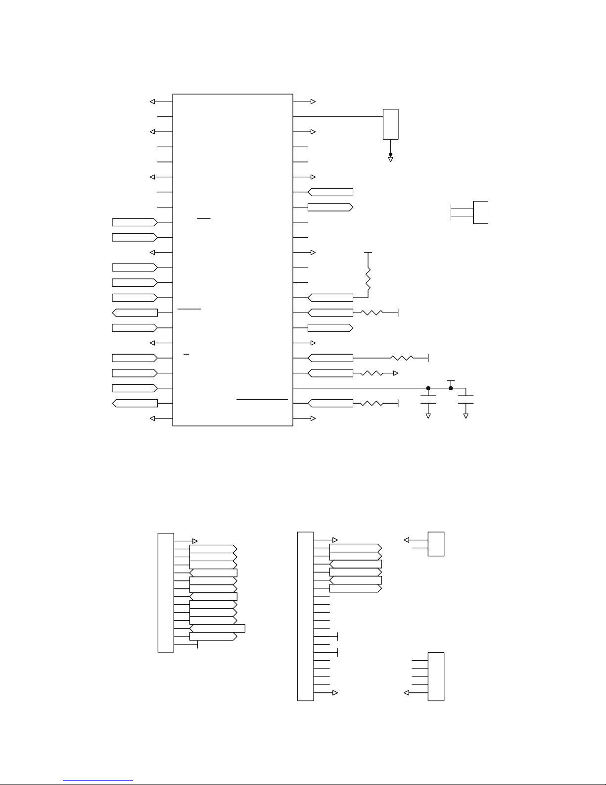
Figure 22: Transceiver Area
Figure 23: Header Section
Page 20
– –
Range Test Area
IN
1
VCC
2
GND3NC
4
COM
5
NO
6
U4
MAX4544EUT
T/R_SEL_R
DATA_MT
GND
VCC
DATA_IN_R
DATA_OUT_R
GND
LED
GREEN
R18
620
D0
LED-0805-GRN
VCC
GND
GND
VCC
BUZZER
VCC
GND
GND
VCC
BUZZER
LED
LED
BOARD A =
NS/DNP
BOARD B = 100K
BOARD A =
NS/DNP
BOARD B = 100K
BOARD A = 100K
BOARD B =
NS/DNP
BOARD A = 100K
BOARD B =
NS/DNP
BOARD A =
NS/DNP
BOARD B =
NS/DNP
BOARD A =
NS/DNP
BOARD B =
NS/DNP
BOARD A = 0 ohm
BOARD B =
NS/DNP
BOARD A = 0 ohm
BOARD B =
NS/DNP
BOARD A =
NS/DNP
BOARD B = 0 ohm
BOARD A =
NS/DNP
BOARD B = 0 ohm
D3
D2
D1
D0
R0 R4
R2
R6
R3
R1
R5
R7
S0
S1
S2
S3
GND
BUZZER
B`
4
C
5
C`
6
GND
7
B
3
A`
2
A
1
E
11
F`
12
F
13
VCC
14
E`
10
D
9
D`
8
U3
CD4069UB
BZ1
AUD-S-BUZ-12MM-4K
R16
100K
R17
10k
C4
0.01uF
D10
GND
GND
GND
GND
D3
D2
D1
D0
GND
GND
GND
T/R_SEL_R
DATA_MT
GND
GND
GND
VCC
1
D6
2
D7
3
CRT/LRN
4
ENC_SEL
5
SER_IO
6
CONFIRM
7
TR_PDN
8
TR_SEL
9
TR_DATA
10
D0
11
D1
12
D2
13
MODE_IND
14
SEL_BAUD
15
LATCH
16
D3
17
D4
18
D5
19
GND
20
U2
LICAL-TRC-MT
R8
100K
R9
100K
R10
100K
R11
100K
R12
100K
R14
100K
R15
100K
BLUE
R13
200 ohm
VCC
C12
0.1uF
GND
GND
VCC
R32
0 ohm
R31
NS/DNP
SW11
SW-SMT-SPDT
VCC
BOARD A =
NS/DNP
BOARD B = 0 ohm
BOARD A = 0 ohm
BOARD B =
NS/DNP
R33
R34
Power Area
IN
1
VCC
2
GND3NC
4
COM
5
NO
6
U4
MAX4544EUT
T/R_SEL_R
DATA_MT
GND
VCC
DATA_IN_R
DATA_OUT_R
GND
LED
GREEN
R18
620
D0
LED-0805-GRN
VCC
GND
GND
VCC
BUZZER
VCC
GND
GND
VCC
BUZZER
LED
LED
BOARD A =
NS/DNP
BOARD B = 100K
BOARD A =
NS/DNP
BOARD B = 100K
BOARD A = 100K
BOARD B =
NS/DNP
BOARD A = 100K
BOARD B =
NS/DNP
BOARD A =
NS/DNP
BOARD B =
NS/DNP
BOARD A =
NS/DNP
BOARD B =
NS/DNP
BOARD A = 0 ohm
BOARD B =
NS/DNP
BOARD A = 0 ohm
BOARD B =
NS/DNP
BOARD A =
NS/DNP
BOARD B = 0 ohm
BOARD A =
NS/DNP
BOARD B = 0 ohm
D3
D2
D1
D0
R0 R4
R2
R6
R3
R1
R5
R7
S0
S1
S2
S3
GND
BUZZER
B`
4
C
5
C`
6
GND
7
B
3
A`
2
A
1
E
11
F`
12
F
13
VCC
14
E`
10
D
9
D`
8
U3
CD4069UB
BZ1
AUD-S-BUZ-12MM-4K
R16
100K
R17
10k
C4
0.01uF
GND
VCCM
+
C2
10uF
GND
GND
GND
VCC
GND
J1
PWRJACK
D1
B1
SW1
Vin
1
GND
2
Vout
3
U1
AP1117E50G-13
+
C1
220uF
POWER AREA
1
TP1
TEST POINT
VCC
1
TP2
TEST POINT
GND
S1
1
G1
2
D23S2
4
G2
5
D1
6
U10
DMG1016V
GND
VCCM
VCC2
R24
10K
R27
100k
PDN
D10
GND
GND
GND
GND
D3
D2
D1
D0
GND
GND
GND
T/R_SEL_R
DATA_MT
GND
GND
GND
VCC
1
D6
2
D7
3
CRT/LRN
4
ENC_SEL
5
SER_IO
6
CONFIRM
7
TR_PDN
8
TR_SEL
9
TR_DATA
10
D0
11
D1
12
D2
13
MODE_IND
14
SEL_BAUD
15
LATCH
16
D3
17
D4
18
D5
19
GND
20
U2
LICAL-TRC-MT
R8
100K
R9
100K
R10
100K
R11
100K
R12
100K
R14
100K
R15
100K
BLUE
R13
200 ohm
VCC
C12
0.1uF
GND
GND
VCC
R32
0 ohm
R31
NS/DNP
SW11
SW-SMT-SPDT
VCC
BOARD A =
NS/DNP
BOARD B = 0 ohm
BOARD A = 0 ohm
BOARD B =
NS/DNP
R33
R34
SW9
MODE_SEL
GND
VCC
1
TP5
TEST POINT
GND
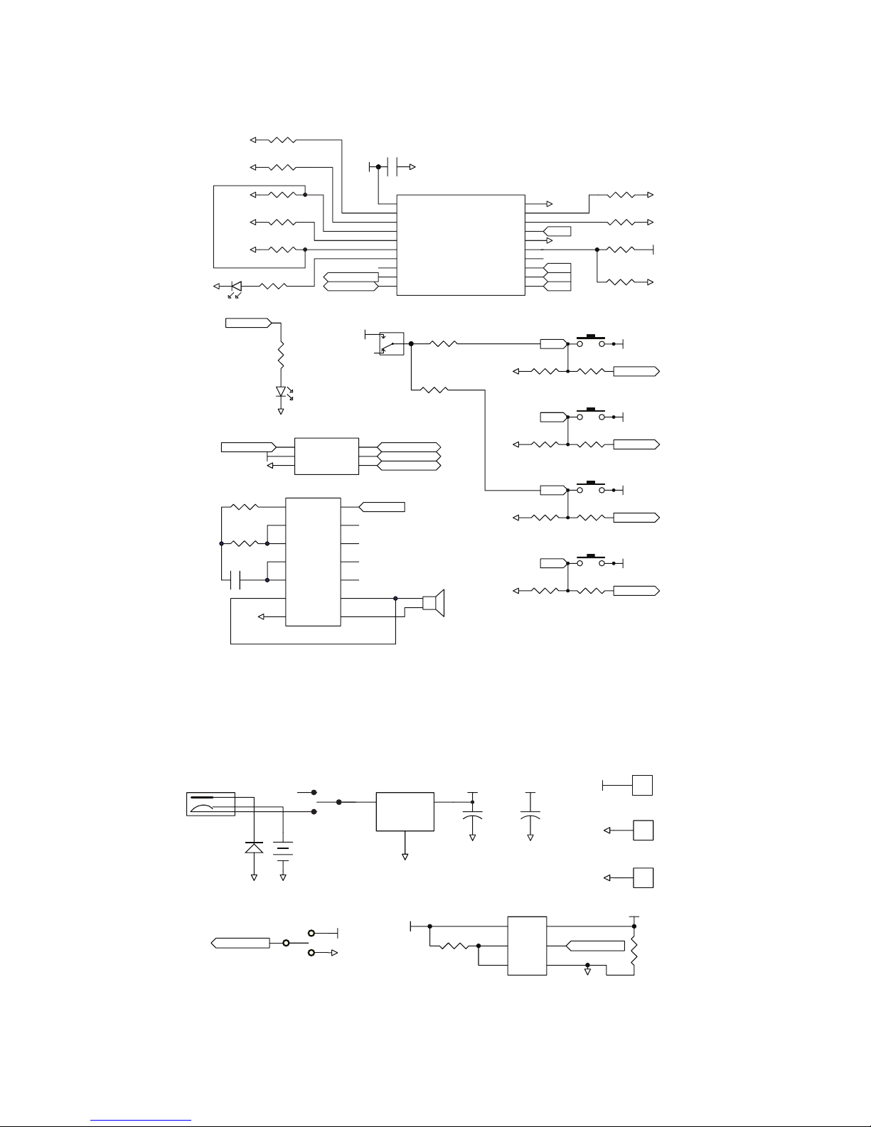
Figure 24: Range Test Area
Figure 25: Power Area
16
Page 21
– –
17
Evaluation Area
EVALUATION AREA SIGNAL ROUTING
1
1
C
2
432
4
C
5
8
6
SW4
GNDGND
CS1_SCS2_S
CS0_S
1
1
C
2
432
4
C
5
8
6
SW5
GNDGND
BAUD1_S
BAUD0_S
SW8
TX_SEL
RNG_SEL
RX_SEL
GND
BAUD1_P
BAUD1_S
Y1
1
Y0
2
Z1
3
Z
4
Z0
5
X0
X1
X
Y
VCC
U7
RSSI
RSSI_P
RSSI_B
C9
0.1uF
GND
R50 NS/DNP
GND
R51 NS/DNP
GND
R52 NS/DNP
GND
R53
GND
5.1M
LEDs
EVALUATION AREA SIGNAL ROUTING
LEDS
1
1
C
2
432
4
C
5
8
6
SW4
GNDGND
CS1_SCS2_S
CS0_S
1
1
C
2
432
4
C
5
8
6
SW5
GNDGND
BAUD1_S
BAUD0_S
ORANGE
D4
R25
200 ohm
GND
TX_LED
D5
R26
200 ohm
YELLOW
GND
RX_LED
GND
R19
620 ohm
ACTV_LED
GREEN
D2
RED
PDN_LED
GND
D7
R40
470 ohm
GND
D3
R38
470 ohm
RED
EVAL_LED
GND
D9
R39
470 ohm
RED
PROTO_LED
STBY_LED
GND
D8
YELLOW
R41
200 ohm
SW8
TX_SEL
RNG_SEL
RX_SEL
GND
CS2
CS1_P
CS1_S
CS2_P
CS2_S
GND
GND
ALL_EN
R44 NS/DNP
GND
R45 NS/DNP
GND
R46 NS/DNP
GND
R47 NS/DNP
GND
ALL_EN
GND
GND
1
2
3
4
5
6
7
8
ALL_EN
DATA_OUT_R
GND
GND
DATA_OUT
DATA_OUT_P
2Y0
1
2Y2
2
2COM
3
2Y3
4
2Y1
5
INH
6
GND
7
GND
8
B
A
1Y3
1Y0
1COM
1Y1
1Y2
VCC
U8
SN74LV4052A
1
TP4
0.1uF
GND
R57
10k
GND
R58
10k
GND
R56
10k
GND
R29
2.20K
GND
1%
LED1
1
V-
2
V+
3
DIVIDER LOW
4
IN
5
DIVIDER HIGH
6
N/C
7
REF OUT
8
N/C9REF ADJ10MODE SELECT
11
LED1012LED9
13
LED8
14
LED7
15
LED6
16
LED5
17
LED4
18
LED3
19
LED2
20
U5
LM3914V
VCC
RSSI_B
GND
GND
+
C5
10uF
GND
R28
1.2K
1%
516
219
318
417
120
615
714
813
912
1011
D6
LED BAR 10
VCC
GND
+
C6
2.2uF
VCC
R42
NS/DNP
BAUD0_P
BAUD0_S
BAUD1_P
BAUD1_S
CH_BD_CTL
GND
GND
VCC
BAUD1
BAUD0
Y1
1
Y0
2
Z1
3
Z
4
Z0
5
EN
6
VEE
7
GND8C
9
B
10
A
11
X0
12
X1
13
X
14
Y
15
VCC
16
U7
MC74HC4053A
ALL_EN
RSSI
RSSI_P
RSSI_B
C9
0.1uF
GND
R50 NS/DNP
GND
R51 NS/DNP
GND
R52 NS/DNP
GND
R53
GND
5.1M
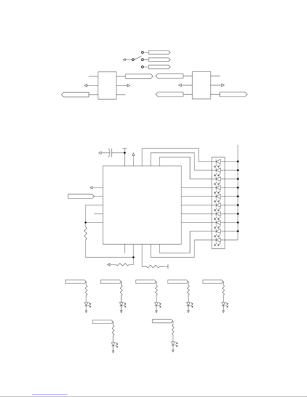
Figure 26: Evaluation Area
Figure 27: LEDs
Page 22
– –
Single Routing
CS1
CS2
CS0
CS0_P
CS0_S
CS1_P
CS1_S
CS2_P
CS2_S
CH_BD_CTL
GND
GND
VCC
Y1
1
Y0
2
Z1
3
Z
4
Z0
5
EN
6
VEE
7
GND8C
9
B
10
A
11
X0
12
X1
13
X
14
Y
15
VCC
16
U6
MC74HC4053A
ALL_EN
C8
0.1uF
GND
R44 NS/DNP
GND
R45 NS/DNP
GND
R46 NS/DNP
GND
R47 NS/DNP
GND
R48 NS/DNP
GND
R49 NS/DNP
GND
T/R_SEL_R
ALL_EN
GND
GND
VCC
T/R_SEL
2Y0
1
2Y2
2
2COM
3
2Y3
4
2Y1
5
INH
6
GND
7
GND
8
B
9
A
10
1Y3
11
1Y0
12
1COM
13
1Y1
14
1Y2
15
VCC
16
U9
SN74LV4052A
TR_CTL1
TR_CTL2
T/R_SEL_P
VCC
GND
C11
0.1uF
GND
R62
NS/DNP
GND
R63
NS/DNP
GND
ALL_EN
DATA_IN_R
DATA_OUT_R
GND
GND
VCC
DATA_OUT
DATA_IN
DATA_OUT_P
DATA_IN_P
DATA_CTL1
DATA_CTL2
2Y0
1
2Y2
2
2COM
3
2Y3
4
2Y1
5
INH
6
GND
7
GND
8
B
9
A
10
1Y3
11
1Y0
12
1COM
13
1Y1
14
1Y2
15
VCC
16
U8
SN74LV4052A
1
TP3
1
TP4
C10
0.1uF
GND
R57
10k
GND
R58
10k
GND
R56
10k
GND
R59
10k
R60
10k
R61
10k
GND
GND
GND
BAUD0_P
BAUD0_S
BAUD1_P
BAUD1_S
CH_BD_CTL
GND
GND
VCC
BAUD1
BAUD0
Y1
1
Y0
2
Z1
3
Z
4
Z0
5
EN
6
VEE
7
GND8C
9
B
10
A
11
X0
12
X1
13
X
14
Y
15
VCC
16
U7
MC74HC4053A
ALL_EN
RSSI
RSSI_P
RSSI_B
C9
0.1uF
GND
R54 NS/DNP
GND
R55 NS/DNP
GND
R50 NS/DNP
GND
R51 NS/DNP
GND
R52 NS/DNP
GND
R53
GND
5.1M
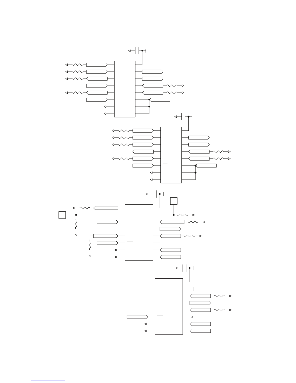
Figure 28: Single Routing
18
Page 23
– –
19
Online Resources
www.linxtechnologies.com
If you have questions regarding any Linx product and have Internet access,
make www.linxtechnologies.com your first stop. Day or night, the Linx
website gives you instant access to the latest information regarding the
products and services of Linx. It’s all here, including:
• Manual and Software Updates
• Latest News
• Data Guides
• Application Notes
• Knowledgebase
• FCC Information
And much more. Be sure to visit often!
www.antennafactor.com
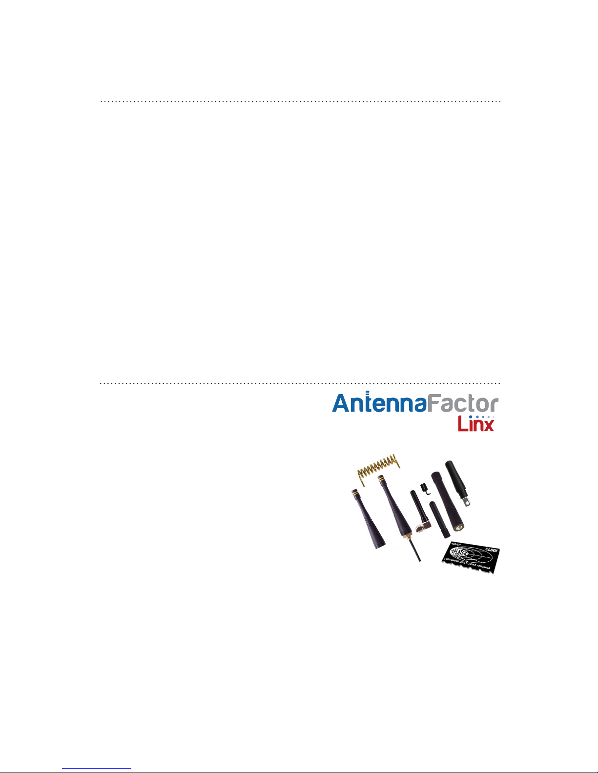
The Antenna Factor division of Linx offers a
diverse array of antenna styles (Figure 29),
many of which are optimized for use with
our RF modules. From innovative
embeddable antennas to low-cost whips,
domes to Yagis, and even GPS, Antenna
Factor likely has an antenna for you, or can
design one to meet your requirements.
Figure 29: Antenna Factor Anetnnas
by
Page 24

Linx Technologies
159 Ort Lane
Merlin, OR, US 97532
3090 Sterling Circle, Suite 200
Boulder, CO 80301
Phone: +1 541 471 6256
Fax: +1 541 471 6251
www.linxtechnologies.com
Disclaimer
Linx Technologies is continually striving to improve the quality and function of its products. For this reason, we
reserve the right to make changes to our products without notice. The information contained in this Data Guide
is believed to be accurate as of the time of publication. Specifications are based on representative lot samples.
Values may vary from lot-to-lot and are not guaranteed. “Typical” parameters can and do vary over lots and
application. Linx Technologies makes no guarantee, warranty, or representation regarding the suitability of any
product for use in any specific application. It is Customer’s responsibility to verify the suitability of the part for the
intended application. At Customer’s request, Linx Technologies may provide advice and assistance in designing
systems and remote control devices that employ Linx Technologies RF products, but responsibility for the ultimate
design and use of any such systems and devices remains entirely with Customer and/or user of the RF products.
LINX TECHNOLOGIES DISCLAIMS ANY AND ALL WARRANTIES OF MERCHANTABILITY AND FITNESS FOR A
PARTICULAR PURPOSE. IN NO EVENT SHALL LINX TECHNOLOGIES BE LIABLE FOR ANY CUSTOMER’S OR
USER’S INCIDENTAL OR CONSEQUENTIAL DAMAGES ARISING OUT OF OR RELATED TO THE DESIGN OR USE
OF A REMOTE CONTROL SYSTEM OR DEVICE EMPLOYING LINX TECHNOLOGIES RF PRODUCTS OR FOR ANY
OTHER BREACH OF CONTRACT BY LINX TECHNOLOGIES. CUSTOMER AND/OR USER ASSUME ALL RISKS
OF DEATH, BODILY INJURIES, OR PROPERTY DAMAGE ARISING OUT OF OR RELATED TO THE USE OF LINX
TECHNOLOGIES RF PRODUCTS, INCLUDING WITH RESPECT TO ANY SERVICES PROVIDED BY LINX RELATED
TO THE USE OF LINX TECHNOLOGIES RF PRODUCTS. LINX TECHNOLOGIES SHALL NOT BE LIABLE UNDER ANY
CIRCUMSTANCES FOR A CUSTOMER’S, USER’S, OR OTHER PERSON’S DEATH, BODILY INJURY, OR PROPERTY
DAMAGE ARISING OUT OF OR RELATED TO THE DESIGN OR USE OF A REMOTE CONTROL SYSTEM OR DEVICE
EMPLOYING LINX TECHNOLOGIES RF PRODUCTS.
The limitations on Linx Technologies’ liability are applicable to any and all claims or theories of recovery asserted
by Customer, including, without limitation, breach of contract, breach of warranty, strict liability, or negligence.
Customer assumes all liability (including, without limitation, liability for injury to person or property, economic loss,
or business interruption) for all claims, including claims from third parties, arising from the use of the Products.
Under no conditions will Linx Technologies be responsible for losses arising from the use or failure of the device
in any application, other than the repair, replacement, or refund limited to the original product purchase price.
Devices described in this publication may contain proprietary, patented, or copyrighted techniques, components,
or materials.
All rights reserved. ©2013 Linx Technologies
The stylized Linx logo, Wireless Made Simple, CipherLinx, WiSE and the stylized CL logo are trademarks of Linx Technologies.
 Loading...